냪ꗟꗦ덱ꑪ뻇 - National Chiao Tung University · Figure 1-4-6 (a) Preparation of...
136
國立交通大學 材料科學與工程學系 博士論文 探討金及硒化鎘奈米粒子自身組織排列於 PS-b-P4VP 雙塊式高分子薄膜之 P4VP 區塊中 之集合電子傳導性質 Collective Electron Transport in Au and CdSe Nanoparticles Self-Assembled in the Poly(4-vinylpyridine) Nanodomains of a Poly(styrene-b-4-vinylpyridine) Diblock Copolymer Thin Film 研究生: 李中斌(Chung-Ping Li) 指導教授: 韋光華(Kung-Hwa Wei) 中華民國 九十五年 五月
Transcript of 냪ꗟꗦ덱ꑪ뻇 - National Chiao Tung University · Figure 1-4-6 (a) Preparation of...
國立交通大學
材料科學與工程學系
博士論文
探討金及硒化鎘奈米粒子自身組織排列於
PS-b-P4VP雙塊式高分子薄膜之P4VP區塊中
之集合電子傳導性質
Collective Electron Transport in Au and CdSe Nanoparticles Self-Assembled in the
Poly(4-vinylpyridine) Nanodomains of a Poly(styrene-b-4-vinylpyridine) Diblock Copolymer
Thin Film
研究生: 李中斌 (Chung-Ping Li) 指導教授: 韋光華 (Kung-Hwa Wei)
中華民國 九十五年 五月
I
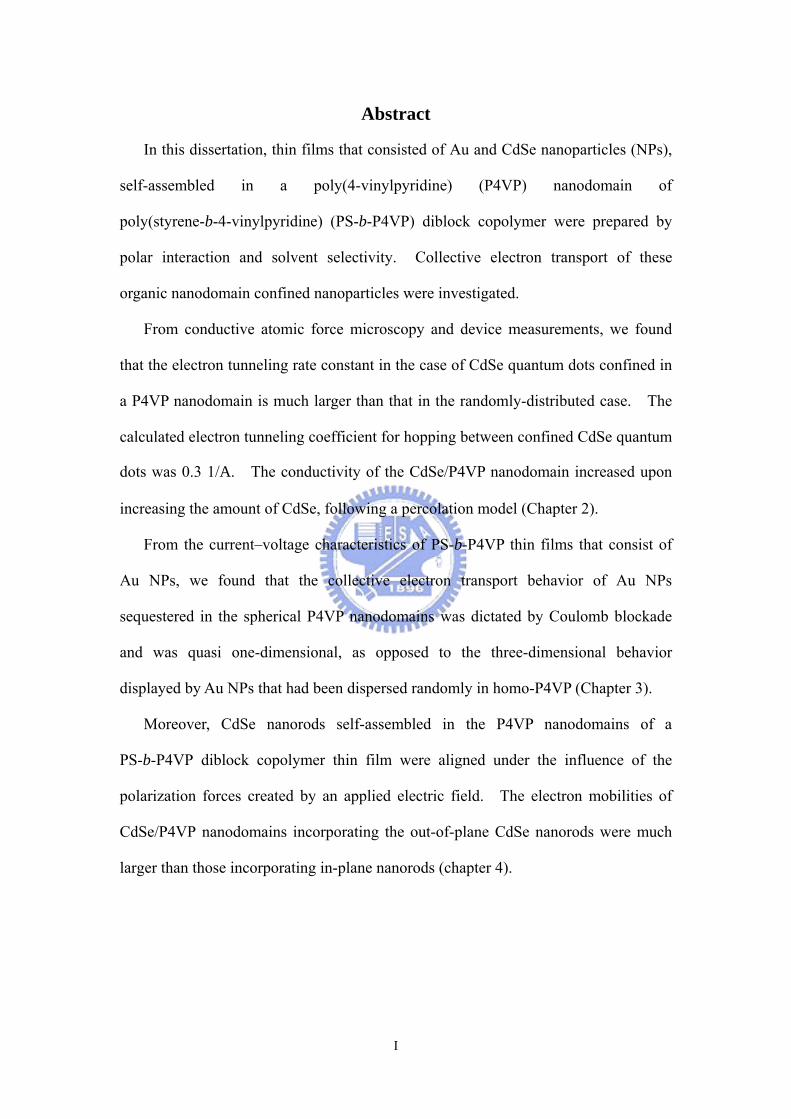
Abstract
In this dissertation, thin films that consisted of Au and CdSe nanoparticles (NPs),
self-assembled in a poly(4-vinylpyridine) (P4VP) nanodomain of
poly(styrene-b-4-vinylpyridine) (PS-b-P4VP) diblock copolymer were prepared by
polar interaction and solvent selectivity. Collective electron transport of these
organic nanodomain confined nanoparticles were investigated.
From conductive atomic force microscopy and device measurements, we found
that the electron tunneling rate constant in the case of CdSe quantum dots confined in
a P4VP nanodomain is much larger than that in the randomly-distributed case. The
calculated electron tunneling coefficient for hopping between confined CdSe quantum
dots was 0.3 1/A. The conductivity of the CdSe/P4VP nanodomain increased upon
increasing the amount of CdSe, following a percolation model (Chapter 2).
From the current–voltage characteristics of PS-b-P4VP thin films that consist of
Au NPs, we found that the collective electron transport behavior of Au NPs
sequestered in the spherical P4VP nanodomains was dictated by Coulomb blockade
and was quasi one-dimensional, as opposed to the three-dimensional behavior
displayed by Au NPs that had been dispersed randomly in homo-P4VP (Chapter 3).
Moreover, CdSe nanorods self-assembled in the P4VP nanodomains of a
PS-b-P4VP diblock copolymer thin film were aligned under the influence of the
polarization forces created by an applied electric field. The electron mobilities of
CdSe/P4VP nanodomains incorporating the out-of-plane CdSe nanorods were much
larger than those incorporating in-plane nanorods (chapter 4).
II
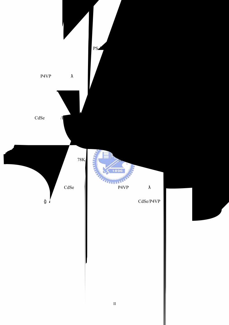
摘要
此論文主旨為利用有機 PS-b-P4VP 雙塊式高分子薄膜自身組織成週期性結
構的特性作為模版並以選擇性分散之技術,分別將無機 Au、CdSe奈米粒子侷限
於 P4VP奈米區塊中形成特定結構之奈米陣列,並探討此具有奈米侷限效應之奈
米粒子之群體電子傳導特性。
利用導電的原子力顯微鏡及電性量測儀器,針對於具有奈米侷限效應之
CdSe 量子點/P4VP 奈米區塊進行量測,發現電子在此具奈米侷限效應之量子點
間之傳導速度遠較不具侷限效應之量子點之傳導速度快。
利用低溫電性量測儀器,針對於具有奈米侷限效應之 Au奈米粒子/P4VP奈
米區塊進行量測,在 78K之低溫量測下,Au奈米粒子具有庫侖阻塞效應,進而
發現具有奈米侷限之奈米粒子呈現出趨近於一維電子傳導之特性。
此外,將 CdSe奈米柱選擇性分散於 P4VP奈米區塊中並在高溫下加入電場
作為驅動力,製備出具方向性且大面積規則排列之 CdSe/P4VP 陣列,並量測加
入電場前後之電子遷移速率。
III
Table of Content Abstract ..............................................................................................................Ⅰ 摘要.......................................................................................................................Ⅱ Chapter 1: Introduction 1-1 Block Copolymers .........................................................................................1 1-2 Nanostructured Materials ..........................................................................12 1-3 Motivation and Scope of Dissertation .......................................................21 Chapter 2: Basic Electron Transport Theory 2-1 Introduction .................................................................................................48 2-2 Conduction Mechanisms ............................................................................48 2-3 Alkanethiol Self-assembled Monolayers Metal-Insulator-Metal Tunneling
.......................................................................................................................49 Chapter 3: Enhanced Collective Electron Transport by CdSe Quantum Dots
Self-Assembled in the Poly(4-vinylpyridine) Nanodomains of a Poly(styrene-b-4-vinylpyridine) Diblock Copolymer Thin Film
3-1 Introduction ................................................................................................54 3-2 Methods and Analysis ................................................................................55 3-3 Results and Discussions .............................................................................57 3-4 Conclusions .................................................................................................65 Chapter 4: Collective Electron Transport in Au Nanoparticles Self-Assembled in
the Poly(4-vinylpyridine) Nanodomains of a Poly(styrene-b-4-vinylpyridine) Diblock Copolymer Thin Film
4-1 Introduction ................................................................................................75 4-2 Methods and Analysis ................................................................................76 4-3 Results and Discussions ...............................................................................78 4-4 Conclusions .................................................................................................83 Chapter 5: The Orientation of CdSe Nanorods Affects the Electron Mobility of
CdSe/P4VP Nanodomains Self-Assembled within a Poly(styrene-b-4-vinylpyridine) Diblock Copolymer Thin Film
5-1 Introduction ...............................................................................................93 5-2 Methods and Analysis ...............................................................................94

IV
5-3 Results and Discussions ............................................................................96 5-4 Conclusions ..............................................................................................101 Chapter 6: Conclusions ...................................................................................109
Chapter 7: References .....................................................................................110

V
Figure List
Chapter 1: Introduction
Figure 1-1-1 Schematic phase diagram showing the various ‘classical’ block
copolymer morphologies adopted by linear diblock copolymer...............................24
Figure 1-1-2 Schematic of morphologies for linear ABC triblock copolymer. A
combination of block sequence (ABC, ACB, BAC), composition and block molecular
weights provides an enormous parameter space for the creation of new morphologies
...................................................................................................................................25
Figure 1-2-1 The well-known structures of block copolymers in melt, solution or
solid state ..................................................................................................................26
Figure 1-3-1 Schematic of various applications of block copolymers in
nanotechnologies.......................................................................................................27
Figure 1-3-2 Schematic of the production process of a metal nanodot array using
block copolymer lithography ....................................................................................28
Figure 1-3-3 SEM image of polystyrene-b-polyferrocenyldimethylsilane mask, after
the polystyrene has been removed by O2 RIE ..........................................................29
Figure 1-3-4 Schematic representation of high density nanowire fabrication in a
polystyrene-b-poly(methylmethacrylate) matrix ......................................................30
Figure 1-3-5 The morphological transformation from a hexagonally packed cylinder
structure of pure polystyrene-b-poly(4-vinylpyridine) (PS-b-P4VP) diblock
copolymers to lamellar (CdS/P4VP)-b-PS composites.............................................31
Figure 1-3-6 Schematic of selectived distribution of TiO2 nanoparticles in
polystyrene-b-poly(methylmethacrylate) diblock copolymer...................................32
Figure 1-3-7 (a) Secondary electron SEM image of the surface of a thin film of a
diblock copolymer–CdSe nanoparticle mixture spin-coated onto a silicon wafer and
annealed at 170 ℃ for 2 days (image width, 250 nm) taken at 1-kV acceleration
voltage. (b) Schematic representation of nanoparticle assembly at the
poly(2-vinylpyridine) cylinders. ...............................................................................33

VI
Figure 1-3-8 TEM micrograph of a ternary blend of polystyrene-b-poly(ethylene
propylene) + AuR1 + SiO2R2 with inorganic filling fraction f = 0:02; respectively,
after micro-sectioning normal to the layer direction (no stain) ................................34
Figure 1-3-9 (a) Assembly of Au nanoparticles (core: 3.9 ± 1.0 nm; shell: polystyrene;
(core+shell)=7.7 nm) into polystyrene-b-poly(2-vinylpyridine) diblock copolymers.
(b) Assembly of Au nanoparticles (core: 3.9 ± 1.0 nm; shell: polystyrene and
poly(2-vinylpyridine); (core+shell)=7.7 nm) into polystyrene-b-poly(2-vinylpyridine)
diblock copolymers. (c), (d) The respective histograms of particle locations for the
samples shown in (a) and (b). Reprinted with permission........................................35
Figure 1-3-10 Cross-sectional transmission electron micrograph showing Au
nanoparticles patterned within the poly(4-vinylpyridine) lamellae formed by a
polystyrene-b-poly(4-vinylpyridine) diblock copolymer ..........................................36
Figure 1-3-11 Schematic of synthesis of needle-like TiO2 nanostructures with ordered
patterns.......................................................................................................................37
Figure 1-3-12 SEM image of an etched polystyrene-b-polyisoprene diblock, showing
a fracture surface. The polystyrene network channels remaining after removal of
polyisoprene are clearly visible ................................................................................38
Figure 1-4-1 Schematic illustration the density of state in semiconductors. ...........39
Figure 1-4-2 EL spectra collected on ITO/PPV (400 Å)/CdSe(CdS)/Mg/Ag devices
having average nanocrystal layer thicknesses of 100 (a), 200 (b), and 400 Å (c). (d)
Show the voltage dependence of the ratio of integrated nanocrystal EL to integrated
PPV EL for the device shown in (b) .........................................................................40
Figure 1-4-3 (a) The structure of regioregular P3HT. (b) The schematic energy level
diagram for CdSe nanorods and P3HT showing the charge transfer of electrons to
CdSe and holes to P3HT. (c) The device structure consists of a film ;200 nm in
thickness sandwiched between an aluminum electrode and a transparent conducting
electrode of PEDOT:PSS..........................................................................................41
Figure 1-4-4 I-V curve of Al/Au-2NT NPs+PS/ Al. The arrows indicate the
biasscanning directions and the inset the device structure........................................42
VII
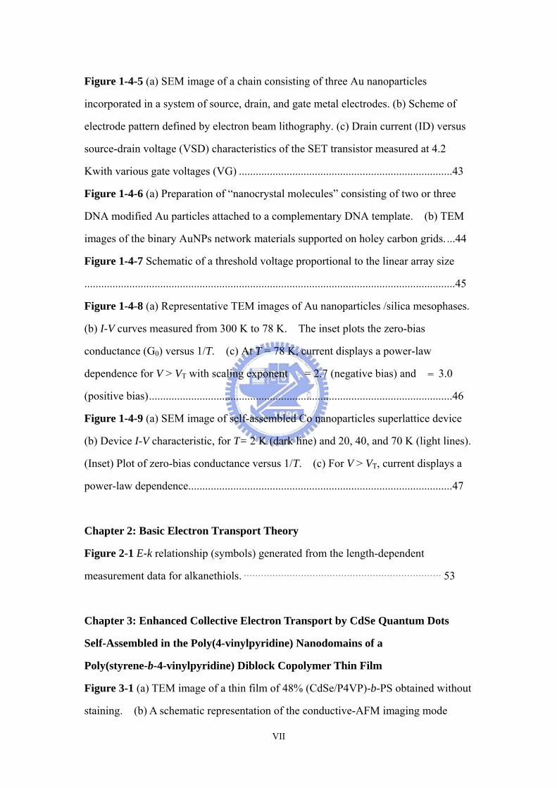
Figure 1-4-5 (a) SEM image of a chain consisting of three Au nanoparticles
incorporated in a system of source, drain, and gate metal electrodes. (b) Scheme of
electrode pattern defined by electron beam lithography. (c) Drain current (ID) versus
source-drain voltage (VSD) characteristics of the SET transistor measured at 4.2
Kwith various gate voltages (VG) ............................................................................43
Figure 1-4-6 (a) Preparation of “nanocrystal molecules” consisting of two or three
DNA modified Au particles attached to a complementary DNA template. (b) TEM
images of the binary AuNPs network materials supported on holey carbon grids....44
Figure 1-4-7 Schematic of a threshold voltage proportional to the linear array size
....................................................................................................................................45
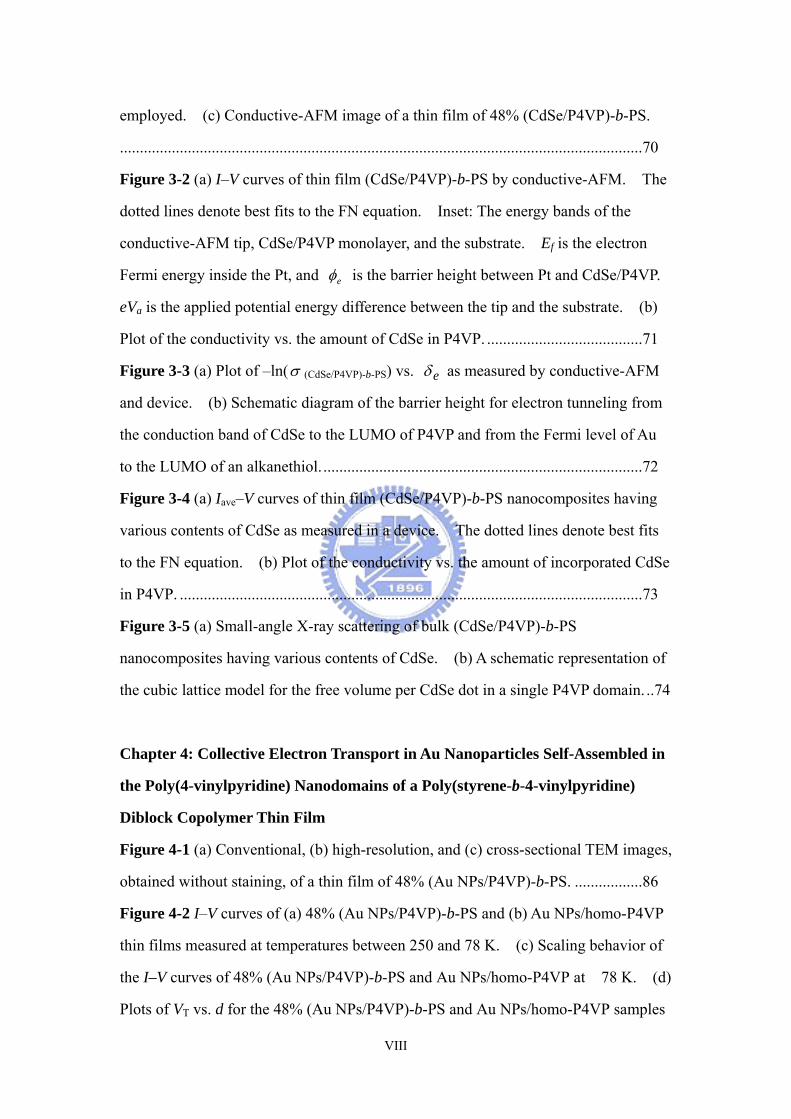
Figure 1-4-8 (a) Representative TEM images of Au nanoparticles /silica mesophases.
(b) I-V curves measured from 300 K to 78 K. The inset plots the zero-bias
conductance (G0) versus 1/T. (c) At T = 78 K, current displays a power-law
dependence for V > VT with scaling exponent ζ= 2.7 (negative bias) andζ= 3.0
(positive bias)............................................................................................................46
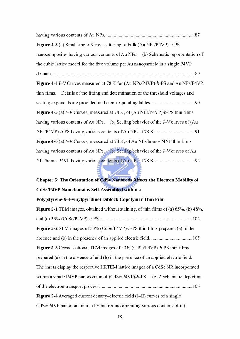
Figure 1-4-9 (a) SEM image of self-assembled Co nanoparticles superlattice device
(b) Device I-V characteristic, for T= 2 K (dark line) and 20, 40, and 70 K (light lines).
(Inset) Plot of zero-bias conductance versus 1/T. (c) For V > VT, current displays a
power-law dependence..............................................................................................47
Chapter 2: Basic Electron Transport Theory
Figure 2-1 E-k relationship (symbols) generated from the length-dependent
measurement data for alkanethiols. ····································································· 53
Chapter 3: Enhanced Collective Electron Transport by CdSe Quantum Dots
Self-Assembled in the Poly(4-vinylpyridine) Nanodomains of a
Poly(styrene-b-4-vinylpyridine) Diblock Copolymer Thin Film
Figure 3-1 (a) TEM image of a thin film of 48% (CdSe/P4VP)-b-PS obtained without
staining. (b) A schematic representation of the conductive-AFM imaging mode
VIII
employed. (c) Conductive-AFM image of a thin film of 48% (CdSe/P4VP)-b-PS.
...................................................................................................................................70
Figure 3-2 (a) I–V curves of thin film (CdSe/P4VP)-b-PS by conductive-AFM. The
dotted lines denote best fits to the FN equation. Inset: The energy bands of the
conductive-AFM tip, CdSe/P4VP monolayer, and the substrate. Ef is the electron
Fermi energy inside the Pt, and eφ is the barrier height between Pt and CdSe/P4VP.
eVa is the applied potential energy difference between the tip and the substrate. (b)
Plot of the conductivity vs. the amount of CdSe in P4VP. .......................................71
Figure 3-3 (a) Plot of –ln(σ (CdSe/P4VP)-b-PS) vs. eδ as measured by conductive-AFM
and device. (b) Schematic diagram of the barrier height for electron tunneling from
the conduction band of CdSe to the LUMO of P4VP and from the Fermi level of Au
to the LUMO of an alkanethiol. ................................................................................72
Figure 3-4 (a) Iave–V curves of thin film (CdSe/P4VP)-b-PS nanocomposites having
various contents of CdSe as measured in a device. The dotted lines denote best fits
to the FN equation. (b) Plot of the conductivity vs. the amount of incorporated CdSe
in P4VP. ....................................................................................................................73
Figure 3-5 (a) Small-angle X-ray scattering of bulk (CdSe/P4VP)-b-PS
nanocomposites having various contents of CdSe. (b) A schematic representation of
the cubic lattice model for the free volume per CdSe dot in a single P4VP domain. ..74
Chapter 4: Collective Electron Transport in Au Nanoparticles Self-Assembled in
the Poly(4-vinylpyridine) Nanodomains of a Poly(styrene-b-4-vinylpyridine)
Diblock Copolymer Thin Film
Figure 4-1 (a) Conventional, (b) high-resolution, and (c) cross-sectional TEM images,
obtained without staining, of a thin film of 48% (Au NPs/P4VP)-b-PS. .................86
Figure 4-2 I–V curves of (a) 48% (Au NPs/P4VP)-b-PS and (b) Au NPs/homo-P4VP
thin films measured at temperatures between 250 and 78 K. (c) Scaling behavior of
the I–V curves of 48% (Au NPs/P4VP)-b-PS and Au NPs/homo-P4VP at 78 K. (d)
Plots of VT vs. d for the 48% (Au NPs/P4VP)-b-PS and Au NPs/homo-P4VP samples
IX
having various contents of Au NPs...........................................................................87
Figure 4-3 (a) Small-angle X-ray scattering of bulk (Au NPs/P4VP)-b-PS
nanocomposites having various contents of Au NPs. (b) Schematic representation of
the cubic lattice model for the free volume per Au nanoparticle in a single P4VP
domain. .....................................................................................................................89
Figure 4-4 I–V Curves measured at 78 K for (Au NPs/P4VP)-b-PS and Au NPs/P4VP
thin films. Details of the fitting and determination of the threshold voltages and
scaling exponents are provided in the corresponding tables.....................................90
Figure 4-5 (a) I–V Curves, measured at 78 K, of (Au NPs/P4VP)-b-PS thin films
having various contents of Au NPs. (b) Scaling behavior of the I–V curves of (Au
NPs/P4VP)-b-PS having various contents of Au NPs at 78 K. ................................91
Figure 4-6 (a) I–V Curves, measured at 78 K, of Au NPs/homo-P4VP thin films
having various contents of Au NPs. (b) Scaling behavior of the I–V curves of Au
NPs/homo-P4VP having various contents of Au NPs at 78 K..................................92
Chapter 5: The Orientation of CdSe Nanorods Affects the Electron Mobility of
CdSe/P4VP Nanodomains Self-Assembled within a
Poly(styrene-b-4-vinylpyridine) Diblock Copolymer Thin Film
Figure 5-1 TEM images, obtained without staining, of thin films of (a) 65%, (b) 48%,
and (c) 33% (CdSe/P4VP)-b-PS. ............................................................................104
Figure 5-2 SEM images of 33% (CdSe/P4VP)-b-PS thin films prepared (a) in the
absence and (b) in the presence of an applied electric field. ..................................105
Figure 5-3 Cross-sectional TEM images of 33% (CdSe/P4VP)-b-PS thin films
prepared (a) in the absence of and (b) in the presence of an applied electric field.
The insets display the respective HRTEM lattice images of a CdSe NR incorporated
within a single P4VP nanodomain of (CdSe/P4VP)-b-PS. (c) A schematic depiction
of the electron transport process. ............................................................................106
Figure 5-4 Averaged current density–electric field (J–E) curves of a single
CdSe/P4VP nanodomain in a PS matrix incorporating various contents of (a)
X
out-of-plane and (b) in-plane CdSe NRs. The dashed lines denote best fits to the FN
equation; the dotted lines denote best fits to the SCLC model, which includes the
field-dependent mobility.........................................................................................107
Figure 5-5 Orientation angle of the protruded CdSe NRs with respect to the plane of
the P4VP-b-PS thin film as function of the electric field strength. ........................108

XI
Scheme & Table List Chapter 2: Basic Electron Transport Theory
Table 2-1 Possible conduction mechanisms. ······················································· 52
Chapter 3: Enhanced Collective Electron Transport by CdSe Quantum Dots
Self-Assembled in the Poly(4-vinylpyridine) Nanodomains of a
Poly(styrene-b-4-vinylpyridine) Diblock Copolymer Thin Film
Scheme 3-1 Fabrication of a self-assembled (CdSe/P4VP)-b-PS thin film by
incorporating selectively dispersed pre-synthesized CdSe QDs in P4VP domain... 66
Table 3-1 Conductivity (σ ) and electron tunneling rate constant ( ETk ) for confined
and non-confined CdSe in P4VP domain as measured by conductive-AFM and in a
device ........................................................................................................................67
Table 3-2 Characteristic Properties of CdSe Quantum Dots....................................68
Table 3-3 Electrical conductivity parameters for the CdSe/P4VP nanodomain.......69
Chapter 4: Collective Electron Transport in Au Nanoparticles Self-Assembled in
the Poly(4-vinylpyridine) Nanodomains of a Poly(styrene-b-4-vinylpyridine)
Diblock Copolymer Thin Film
Scheme 4-1 Fabrication of a self-assembled (Au NPs/P4VP)-b-PS thin film through
the selective incorporation of dispersed pre-synthesized Au NPs into P4VP domains.
..................................................................................................................................84
Table 4-1 Details of the Fitting of I–V Curves, Measured at 78 K, for (Au
NPs/P4VP)-b-PS and Au NPs/P4VP Thin Films Having Various Contents of Au NPs,
and Determination of the Threshold Voltages and Scaling Exponents. ....................85
Chapter 5: The Orientation of CdSe Nanorods Affects the Electron Mobility of
CdSe/P4VP Nanodomains Self-Assembled within a
Poly(styrene-b-4-vinylpyridine) Diblock Copolymer Thin Film
Scheme 5-1 Fabrication of a self-assembled (CdSe/P4VP)-b-PS thin film through the
selective incorporation of dispersed pre-synthesized CdSe NRs into P4VP
nanodomains. ..........................................................................................................102

XII
Table 5-1 Electron barrier heights ( eφ ), electron mobilities ( 0µ ), and field
coefficients ( 0E ) for in-plane and out-of-plane CdSe NRs incorporated within P4VP
nanodomains in a PS matrix. ..................................................................................103
1
Chapter 1 Introduction
1-1 Block Copolymers
A block copolymer (BCP) can self-assemble into an ordered periodic structures
with a nanometer thicknesses that depends on molecular weight, segment size, and the
strength of interaction between the blocks, represented by the Flory–Huggins
interaction parameter, χ. [1–3] The periodicity thickness is in the range 10–200 nm.
The morphology depends on χand the composition of the copolymer, parametrized
as the volume fraction of one of the constituent blocks. For the simplest class of
A-B diblock copolymers, the following structures are known to be stable, as
confirmed by theory [4] and experiment [2, 5]: lamellar, hexagonal-packed cylinder,
body-centred cubic, close-packed spherical (which may exhibit only liquid-like
ordering) and bicontinuous cubic gyroid structures, as shown in Figure 1-1-1. For
ABC triblocks, the combination of two independent composition variables (e.g.
volume fraction fA and fB, fA+ fB+ fC = 1) and three χ parameters (χAB, χAC
and χBC) leads to a much wider range of possible morphologies shown in Figure
1-1-2. Many have been observed, although others await discovery. [6] Theory
provides guidelines for rationalizing the observed morphologies, and in the future
may be used to predict structures. [7]
1-1-1 The Structure of Block Copolymer melts, solids, and solutions
A remarkable property of block copolymers is their ability to self-assemble in the
melt in to a variety of ordered structures with nanoscale periodicities. These
structures can be controlled by varying the composition of the block copolymer or the
segregation between blocks (via temperature or degree of polymerization). In
addition to the now well-established lamellar (lam), hexagonal-packed cylinder(hex)

2
and body-centered cubic (BCC) micelle phase, a number of few morphologies have
been discovered, which supplement the “classical structure”. The identification of a
bicontinuous cubic phase of dIa3 symmetry, sometimes called the gyroid phase, is
now established. Figure 1-2-1 shows the well-known structure of block copolymers
in melt, solution or solid state. [8]
Melts
Two competing effects govern the thermodynamics of block copolymer melts.
At high temperature, the chains are mixtures homogeneously, as in any polymer melt.
As the temperature is reduced, the tendency for the blocks to segregate is enhanced,
i.e. the enthalpic process of demixing is favored. However, this is necessarily
accompanied by a reduction in entropy as the chain configuration becomes more
constrained. The extent of segregation of the copolymer may then be expressed
using the reduced parameterχ N. Here N is the copolymer degree of
polymerizatiom, reflecting the N-dependent translation and configuration entropy.
The segment–segment interaction parameter (Flory–Huggins) described the free
energy cost per monomer of conducts between the A and B monomeric units and is
given by: ( )[ ]2/BBAAABB
AB TZ εεεκχ +−
= , where ABε is the interaction energy
permonomer units between A and B monomers and Z is the number of nearest
neighbor monomers to a copolymer configuration cell. Thus, positive χAB (which
is the vast majority of cases) shows repulsion between the A and B monomers,
whereas a negative value signifies mixing of unlike monomers. Moreover, χAB
usually varies inversely with temperature. The second parameter that strongly
influences the block copolymer behavior is the total degree of polymerization N.
For large N the loss of translational and configurational entropy leads to a reduction

3
of the A-B monomer contacts and thus to local ordering. Since the entropic and
enthalpic contributions to the free energy scale as N-1 and χ, respectively, it is the
product χN that is of interest in the block copolymer phase state.
Solutions
There are two basic processes that characterize the phase behavior of block
copolymers in solution: micellization and gelation. Micellization occurs when block
copolymer chains associate into, often spherical, micelles in dilute solution in a
selective solvent. The core of the micelle is formed by the insoluble or poorly
solvated block, whilst the corona contains the selectively solvated block. At a fixed
temperature, micellization occurs on increasing concentration at the critical micelle
concentration (CMC). The cmc is usually determined from the sharp decrease in the
surface tension as a function of concentration, although other properties such as
viscosity also exhibit pronounced changes.
In concentrated solutions, micelles can order into gels. Soft and hard gels are
distinguished from each other and from micellar solutions by their flow properties,
gels being characterized by a finite yield stress. The hard gels seem to be associated
with the formation of cubic phases of spherical micelles, whereas soft gels are usually
lamellar or hexagonal-packed rod micellar phase. The phase behavior of these
materials has only recently begun to be elucidated using small angle scattering. It
promises to be even richer than that of block copolymer melts, at least if results for
analogous conventional surfactants are any guide. The flow behavior of these gels is
the basis for many of their applications, and study of the rheology and behavior under
shear of these materials will enhance the fundamental understanding underpinning
future developments.
Solids

4
The structure of block copolymer melts is usually trapped upon vitrification. The
mechanism underlying the glass transition are similar to those of the constituent
homopolymers. Thus there are little distinct physicals associated with the formation
of solid phase by glassy block copolymers.
In contrast, crystallization of one or both components of a block copolymer is
accompanied by profound structure and dynamic changes. The fundamental process
in crystallization of chains in a crystallizable block copolymer is the change in block
conformation, i.e. the adoption of an extended or a folded structure rather than a
coiled configuration found in the melt or solution. Crystallization from the melt
often leads to a distinct (usually lamellar) structure, with a different periodicity from
the melt. Crystallization from solution can lead to non-lamellar crystalline structures,
although these may be often be trapped non-equilibrium morphology. In addition to
the formation of extended or folded chains, crystallization may also lead to gross
orientational changes of chains.
1-1-2 Applications
Until recently, most industrial applications of BCPs were as adhesives or for their
mechanical properties (e.g. as thermoplastic elastomers). Only in the past 10 years
have researchers taken BCPs into the “high-technology” area, to the so-called
“nanotechnologies”. Many attempts have been made to utilize BCPs in
nanotechnology. Self assembled BCP microstructures with 10 to 100 nm
dimensions are useful as nanometer scale membranes, templates for fabrication of
nano-objects such as metal, ceramic nanodots and wires, as 1-, 2- and 3D photonic
crystals, and as nanopattern masks for fabrication of high density information storage
media. The majority of applications proposed to date rely on the use of thin film
structures and this is a major focus of the current review, although bulk nanoporous
materials and photonic crystals are considered. The applications of various BCP

5
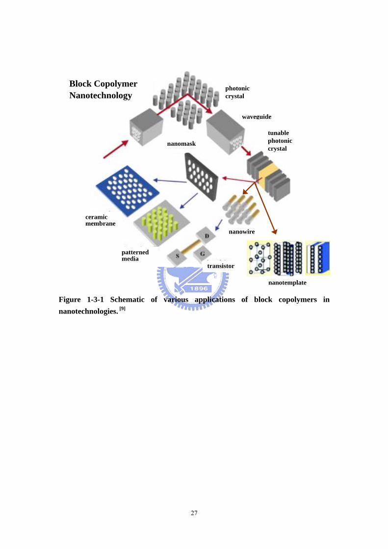
enabled nanotechnologies are summarized in Figure 1-3-1. [9]
Nanolithography
Nanosizes greater than 150 nm can be routinely produced by photolithography
techniques. The minimum size that can be achieved by photolithography is
determined by the wavelength of light used in the exposure. Electron beam
lithography is commonly used to access feature sizes between 150 nm and 30 nm.
However, sizes less than 30 nm are not easily obtained by standard lithography. One
way to overcome this problem is by using self-assembled block copolymers.
In a pioneering paper, Park et al [10] demonstrated the use of block copolymer
films as masks to transfer dot and stripe patterns into semiconductors. The feature
density of holes achieved was ~1011 cm -2. The method they developed relies on the
selective ozonation of polyisoprene (PI) or polybutadiene (PB) in block copolymers
with polystyrene (PS) as the other, majority, component. Ozone cleaves the double
bonds in the unsaturated polymers, so that they can be etched away. This process
leaves holes or stripes in a PS matrix. This pattern was transferred from the block
copolymer into silicon nitride by RIE using CF4 or CF4/O2 gases. The quality of
pattern transfer is excellent, producing nanoscale arrays of pits or channels. Park et
al also discuss how to prepare a nanoscale array of posts by use of an “inverse”mask
to that used to produce the array of pits. If the PI is fixed by staining with osmium
tetroxide, then etching of the matrix will occur preferentially. The regions under the
PI domains will be left as an array of posts. Details of the ozone etching method of
preparing block copolymer film masks were elaborated on in a subsequent paper, [11]
which also contains data illustrating pattern transfer into other semiconductors,
including silicon and germanium. A patent was awarded for this technology in 1999.
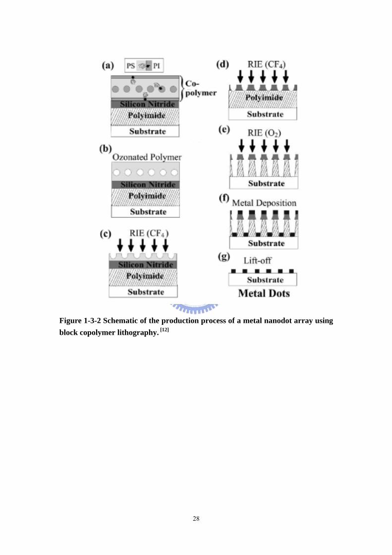
[12] In a further extension of the technique, it has been demonstrated that arrays of
nano-sized metal posts can be fabricated, by an extension of the preceding method,
6
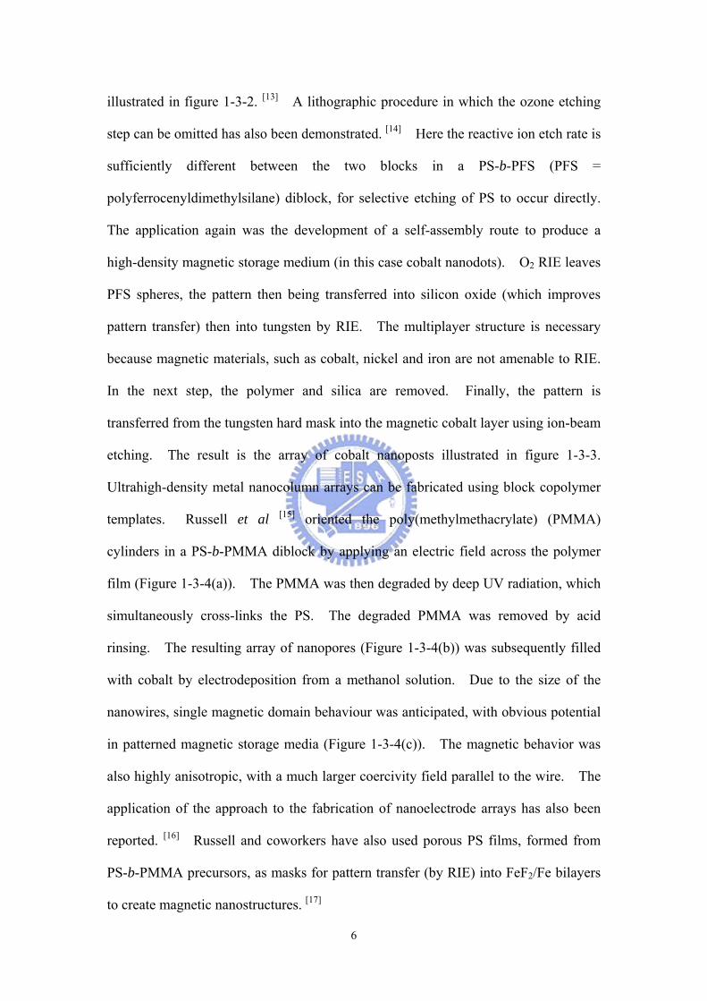
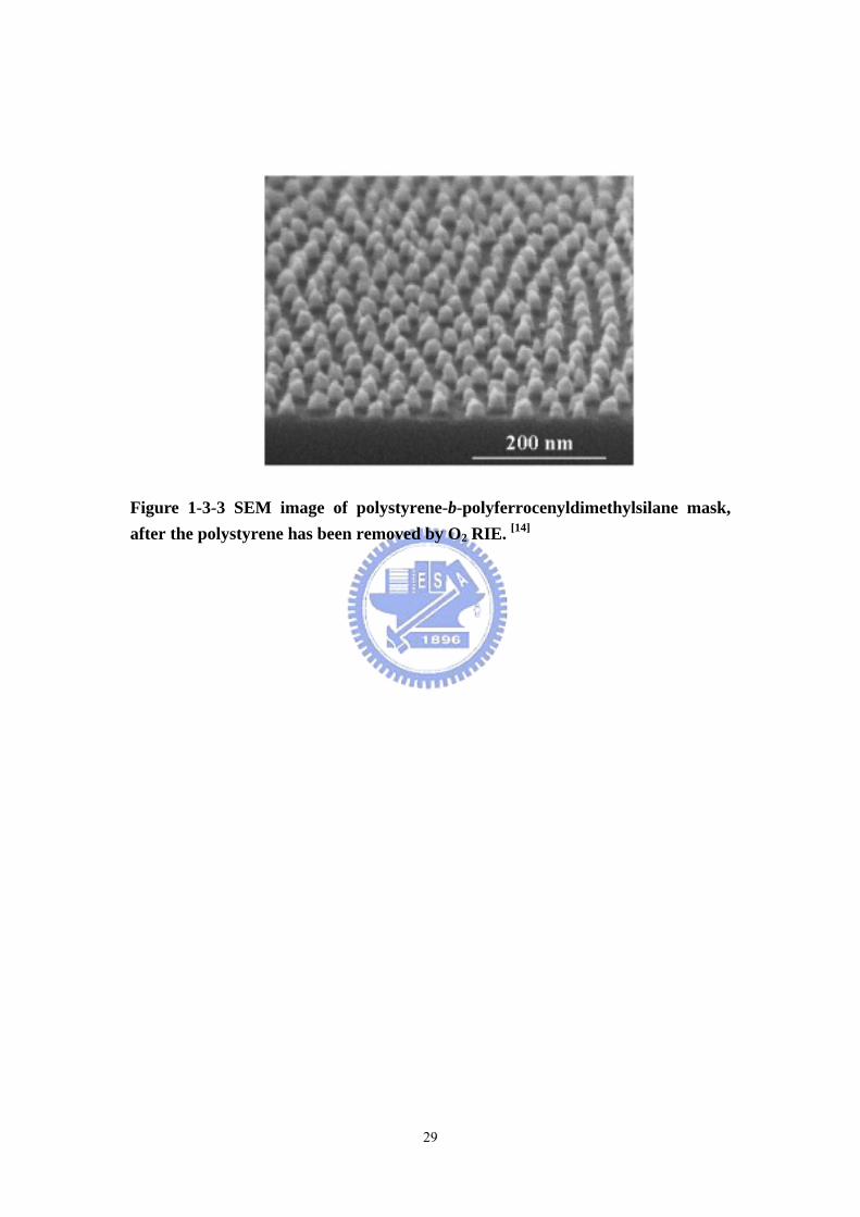
illustrated in figure 1-3-2. [13] A lithographic procedure in which the ozone etching
step can be omitted has also been demonstrated. [14] Here the reactive ion etch rate is
sufficiently different between the two blocks in a PS-b-PFS (PFS =
polyferrocenyldimethylsilane) diblock, for selective etching of PS to occur directly.
The application again was the development of a self-assembly route to produce a
high-density magnetic storage medium (in this case cobalt nanodots). O2 RIE leaves
PFS spheres, the pattern then being transferred into silicon oxide (which improves
pattern transfer) then into tungsten by RIE. The multiplayer structure is necessary
because magnetic materials, such as cobalt, nickel and iron are not amenable to RIE.
In the next step, the polymer and silica are removed. Finally, the pattern is
transferred from the tungsten hard mask into the magnetic cobalt layer using ion-beam
etching. The result is the array of cobalt nanoposts illustrated in figure 1-3-3.
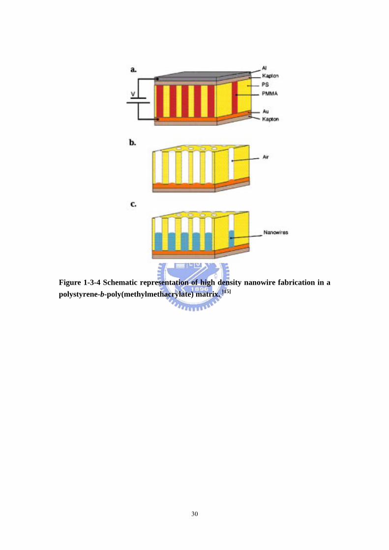
Ultrahigh-density metal nanocolumn arrays can be fabricated using block copolymer
templates. Russell et al [15] oriented the poly(methylmethacrylate) (PMMA)
cylinders in a PS-b-PMMA diblock by applying an electric field across the polymer
film (Figure 1-3-4(a)). The PMMA was then degraded by deep UV radiation, which
simultaneously cross-links the PS. The degraded PMMA was removed by acid
rinsing. The resulting array of nanopores (Figure 1-3-4(b)) was subsequently filled
with cobalt by electrodeposition from a methanol solution. Due to the size of the
nanowires, single magnetic domain behaviour was anticipated, with obvious potential
in patterned magnetic storage media (Figure 1-3-4(c)). The magnetic behavior was
also highly anisotropic, with a much larger coercivity field parallel to the wire. The
application of the approach to the fabrication of nanoelectrode arrays has also been
reported. [16] Russell and coworkers have also used porous PS films, formed from
PS-b-PMMA precursors, as masks for pattern transfer (by RIE) into FeF2/Fe bilayers
to create magnetic nanostructures. [17]
7
Nanoparticle Templates
BCPs have also been utilized not only as surfactants to inhibit coalescence and aid
in dispersion of nanoscale particles such as metal, metal oxide, inorganics, molecular
chromophores and quantum dots but also to spatially pattern the particles.
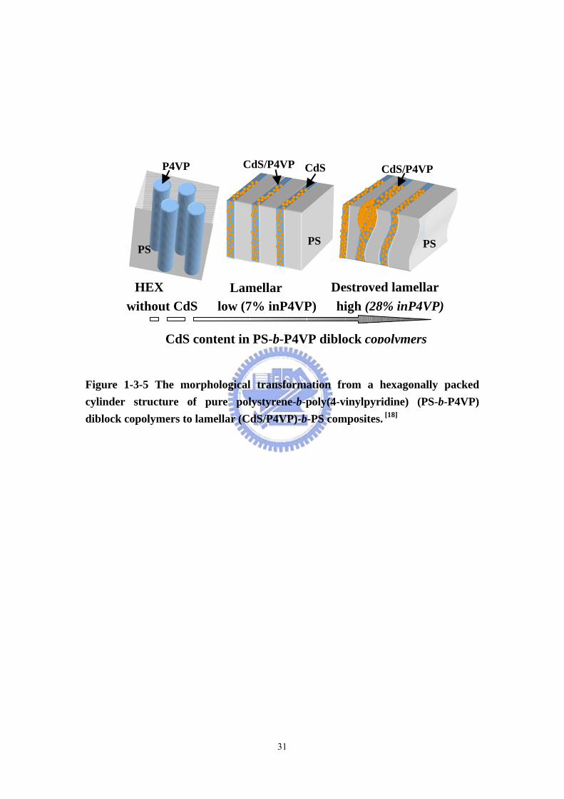
In previous works of our group, we reported a morphological transformation of
PS-b-P4VP (P4VP = poly(4-vinylpyridine)) from a hexagonally packed cylinder
structure to a lamellar structure, which occurred upon sequestering CdS nanoparticles
in the P4VP block. [18] The surface of the CdS nanoparticles was stabilized with
mercaptoacetic acid as a surfactant, which renders each CdS nanoparticle hydrophilic.
Thus, CdS nanoparticles segregated selectively into the P4VP domains due to the
dipole-dipole interactions between the carboxylic acid on the CdS surface and the
P4VP chains. Whereas pure PS-b-P4VP showed a hexagonally packed cylindrical
structure, the composite transformed into a lamellar structure in the presence of 7 wt%
CdS nanoparticles (Figure 1-3-5). The morphological transformation from the
cylindrical to lamellar structure was mediated by strong interaction forces such as
hydrogen bonds between carboxylic acid units of the CdS nanoparticles and the P4VP
chains. In another paper, [19] ordered clusters of surfactant-modified TiO2
nanoparticles in the selective block of lamellar assemblies of the diblock copolymer
PS-b-PMMA have been reported (Figure 1-3-6). Instead of using an water or
alcohol phase, the TiCl4 or tetra(isopropoxide) (TTIP) precursors were used to
synthesize the TiO2 nanoparticles in tetrahydrofuran (THF), which is a good solvent,
for block copolymers. Cetyl trimethyl ammonium chloride (TMAC) amphiphilics or
3-(methacryl loyloxypropyl)-trimethoxy silane (TMS) surfactant was used to modify
the TiO2 nanoparticles. To our knowledge, this presents a new approach to
selectively disperse quantum-confined nanoparticle clusters in a PS-b-PMMA diblock
copolymer with an ordered lamellar phase. 3-D and 2-D nanostructure of CdS
8
clusters by dispersing pre-synthesized CdS nanoparticles, containing hydroxyl groups
on surface, in the PEO block selectively of polystyrene-b-poly(ethylene oxide) (SEO)
block copolymers as template in the bulk form and thin films were reported. [20-24]
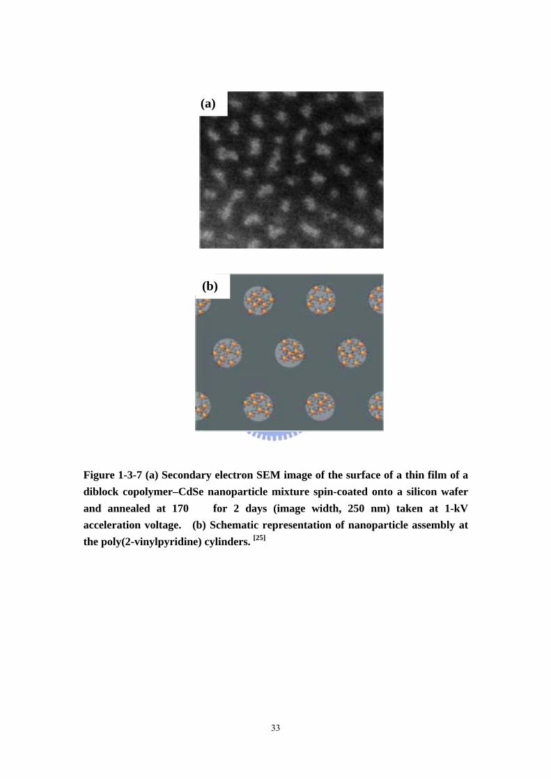
Russell [25] et al. reported that mixtures of diblock copolymers and either cadmium
selenide- or ferritinbased nanoparticles exhibit cooperative, coupled self-assembly on
the nanoscale. In thin films, the copolymers assemble into cylindrical domains,
which dictate the spatial distribution of the nanoparticles; segregation of the particles
to the interfaces mediates interfacial interactions and orients the copolymer domains
normal to the surface, even when one of the blocks is strongly attracted to the
substrate. Organization of both the polymeric and particulate entities is thus
achieved without the use of external fields opening a simple and general route for
fabrication of nanostructured materials with hierarchical order (Figure 1-3-7).
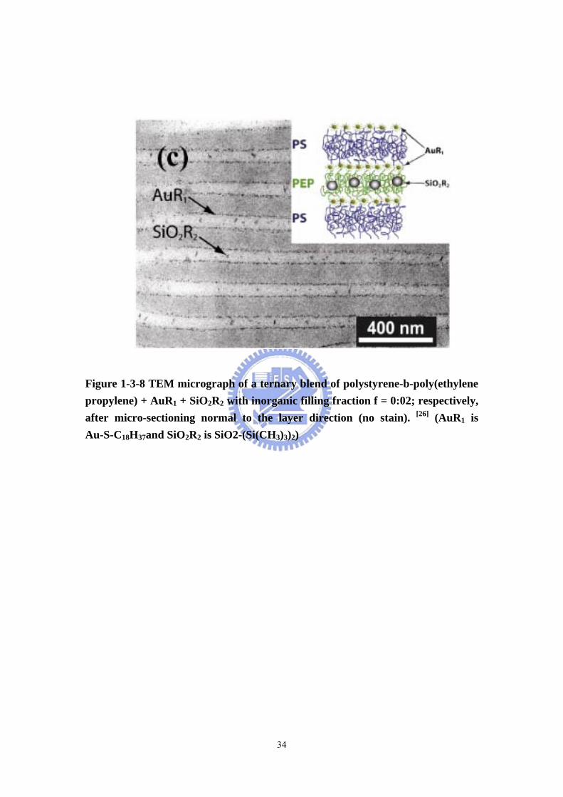
Thomas et al. [26] have identified that the localization of particles along the interface
or at the center of the respective polymer domain was also affected by the
particle-core sizes. In the system consisting of a symmetric PS-b-PEP (PEP =
poly(ethylene propylene)), large silica nanoparticles (d = 21.5 nm; d/L ~ 0.26, where
d is the particle diameter and L is the respective domain dimension of the block
copolymer) were located at the center of the PEP domain. The smaller gold
nanoparticles (d = 3.5 nm, d/L ~ 0.06) segregated at the interface between two block
phases (Figure 1-3-8) in accordance with theoretical simulations. [26] Interfacial
segregation of nanoparticles is expected to occur for particle sizes with d/L<0.2,
whereas localization of nanoparticles at the center of the lamellae phase is expected
for d/L>0.3. Figure 1-3-9a shows a cross-sectional TEM image of 100% PS
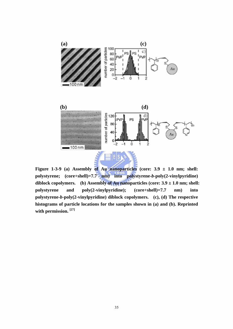
thiol-coated gold nanoparticles dispersed on symmetric PS-b-P2VP block copolymer.
[27] PS-coated gold nanoparticles are located near the center of the PS block phase of
the lamellae structure, whereas poly(2-vinylpyridine) (P2VP)-coated gold
9
nanoparticles were located in the P2VP domain as expected. Particles coated with a
similar homopolymer can lower their enthalpy by segregating into the corresponding
domain of the block copolymer. Positioning the particle near the center of the
corresponding polymer domain leads to a better embedding of the NP since the
polymer chains can accommodate particles by moving apart rather than by stretching.
Particles coated with a mixture of PS and P2VP thiols are exactly localized at the
interface between the PS and P2VP block phases (Figure 1-3-9b).
Nanoreactors for nanostructure production
Block copolymer domains can be used as ‘nanoreactors’ for the synthesis of
inorganic nanoparticles. Reviews of the subject are available. [28, 29] Two basic
approaches have been developed. The first involves the binding of inorganic species
to the monomer prior to polymerization or to one of the blocks of a copolymer prior to
micellization (which may be induced by the ion binding [28]). The most important
approach, however, involves the loading of pre-formed micelles, whether in solution
or in bulk.
Micellar nanoreactors for metallic nanoparticles based around several different
block copolymers have been investigated by Bronstein and coworkers. In many
cases, the ability of poly(vinylpyridine), P2VP or P4VP, to form complexes with
metal salts due to the presence of an N atom is exploited. [30–31] For example,
palladium clusters have been produced by reduction of Pd(CH3COO)2 that
coordinates to the P4VP micellar core formed by PS-b-P4VP diblocks in toluene. [30,
32] Other metal nanoclusters including cobalt, [33] gold, [30, 31, 32] rhodium [30] and
platinum [30] have been prepared in a similar way. The catalytic hydrogenation
properties of the nanoclusters have been compared. [30, 32] Bimetallic colloids have
also been prepared. [30] The methods may be extended to thin films where surface
interactions may be exploited to prepare highly aligned nanostructures. Sohn and
10
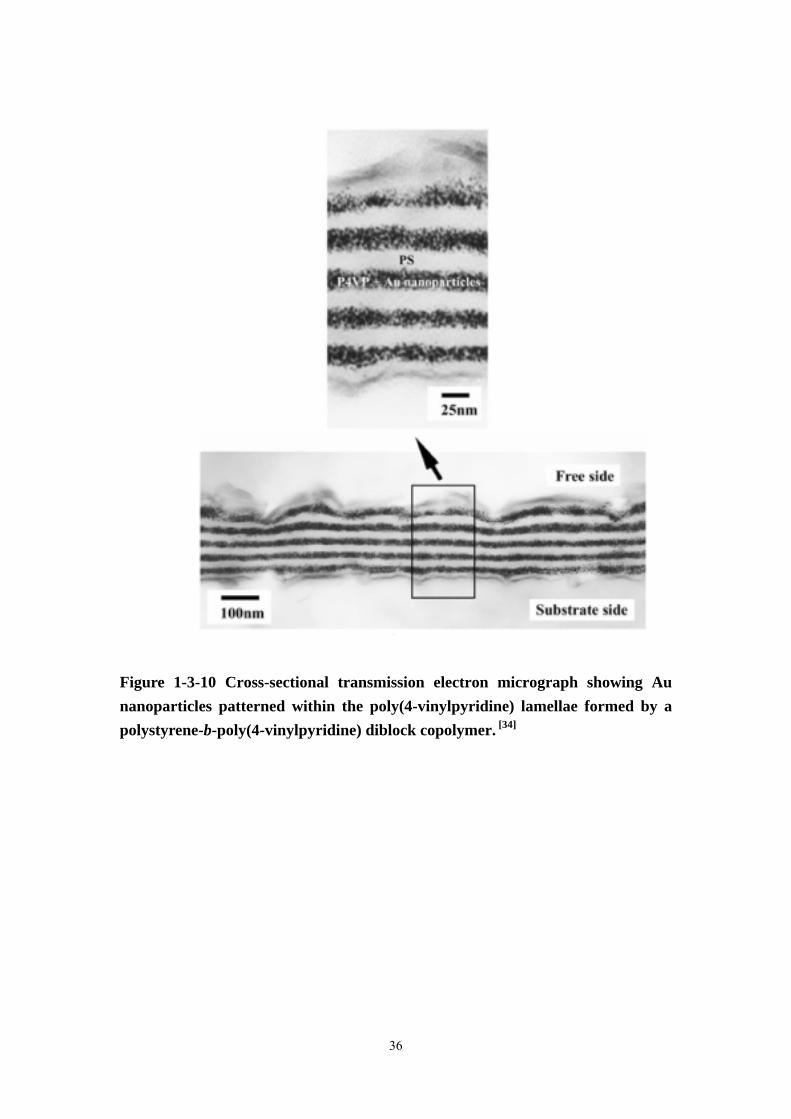
Seo [34] exploited strong preferential interfacial segregation of the blocks in a thin
filmof a PS-b-P4VP diblock to fabricate a multilayer stack consisting of alternating
P4VP lamellae containing gold nanoparticles and nanoparticle-free PS lamellae
(Figure 1-3-10). Titania nanoparticles are interesting for applications such as
catalysis, water purification and UV blocking. Spatz et al [35] have shown how
nanoparticles can be produced within block copolymer micelle nanoreactors. They
prepared micelles from a PS-b-PEO (PEO = poly(ethylene oxide)) diblock in a
non-polar solvent with a PS corona and a PEO core. HCl was mixed with the
micelle solution to create reservoirs within the micelle cores. Titanium alkoxides
were then added, the reaction with the acid and subsequent heating leading to the
formation of TiO2 particles. Individual particles and chains were both obtained. In
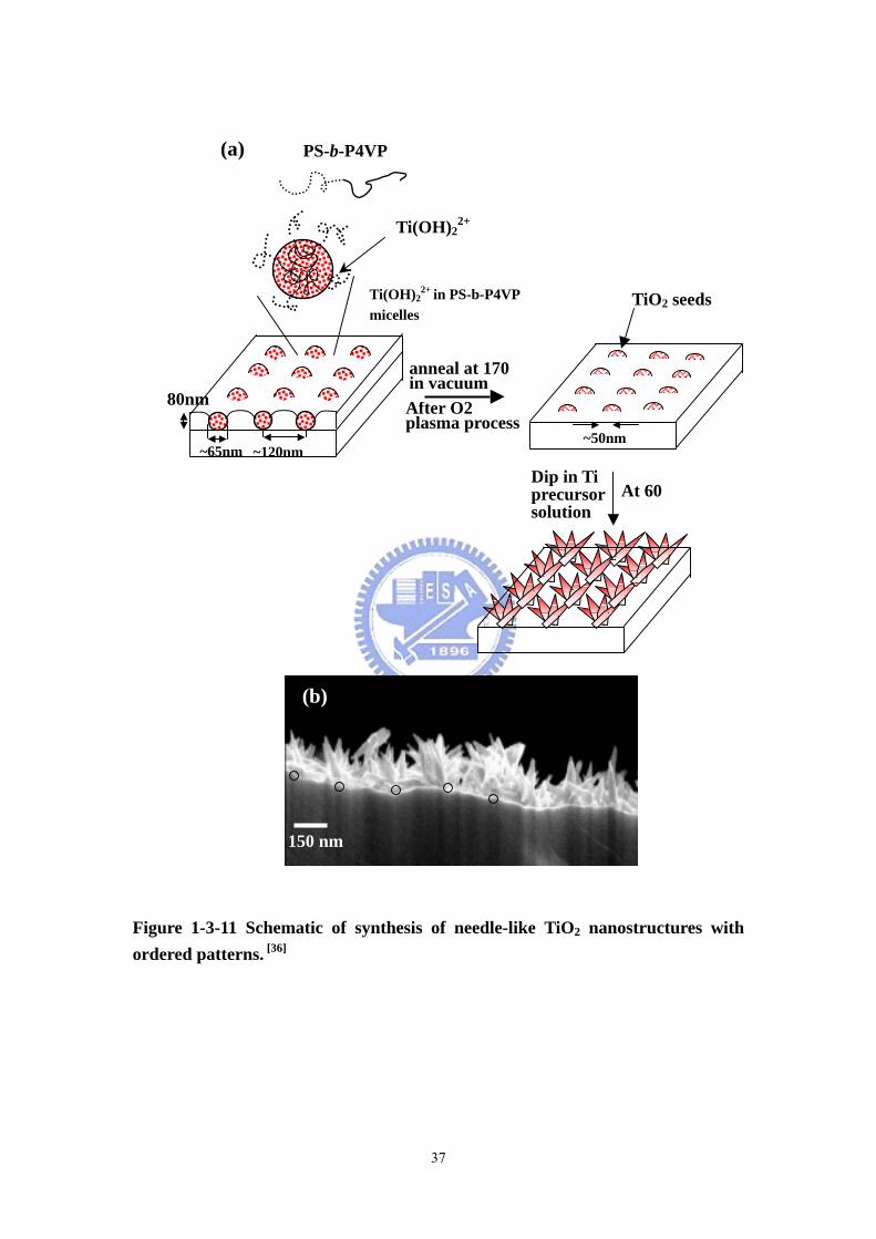
previous works of our group, we have reported synthesis of arrayed, TiO2 needle-like
nanostructures via a PS-b-P4VP diblock copolymer template. [36] Arrayed,
needle-like nanostructures of rutile phase crystal TiO2 were grown on a Si substrate
containing TiO2 seeds prepared through a thin PS-b-P4VP (use unabbreviated name
first) diblock copolymer template. By using TiO2 seeds prepared from their diblock
copolymer PS-b-P4VP template, arranged needle-like rutile TiO2 nanostructures with
variable spatial positions and densities were fabricated. The distance between two
TiO2 needle bunches could be controlled using block copolymer templates with
different molecular weights (120nm and 160 nm) (Figure 1-3-11).
Photonic Crystals
Photonic crystals are attracting immense attention since they can be used to
control and confine light. Materials with a complete bandgap reflect light (incident in
any direction) within the wavelength range of the gap. Block copolymers are
interesting materials with which to construct photonic crystals because they can
self-assemble into periodic structures in one, two and three dimensions. The
11
inherently low dielectric contrast between the polymeric domains can be overcome by
selective doping and/or removal of one component. Another prime constraint is the
requirement for telecommunications applications of a domain size of about 250 nm
(to control near-IR radiation with a wavelength of 1.55 μm). [37] Additionally,
long-range order of the materials must be achieved. Much of the current research
comes from the Thomas group, and they have provided a good review of material
requirements and possibilities, as well as research up to year 2000, [37] this is also
being complemented by an earlier overview. [38]
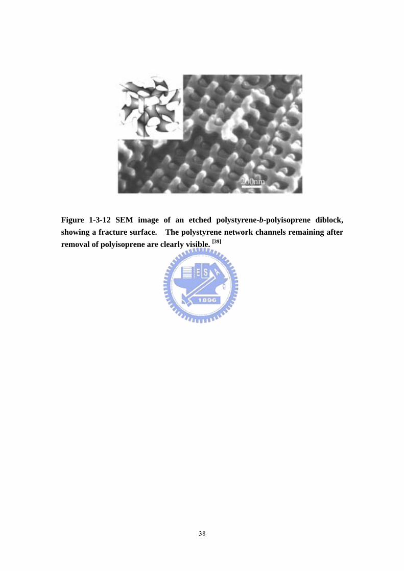
Theory has been used to predict the possibility of photonic bandgaps in single and
double network bicontinuous cubic structures. [39] However, the calculations
indicated that (for the parameter space explored) no complete bandgaps exist for
bicontinuous double primitive, double gyroid (body-centred cubic) or double diamond
(face-centred cubic) structures. However, bandgaps are anticipated for the single
network analogues, the best candidate being a single diamond structure with a
dielectric contrast as low as 3.6. The optical reflectivity characteristics of an
experimentally realized large domain double gyroid structurewere subsequently
assessed. [40] The initial material was a PS-b-PI diblock with high molar mass
leading to a cubic lattice parameter a = 258 nm. The optical properties were
measured for a bulk film, and also for sample in which the PI block was removed by
UV/ozone treatment (Figure 1-3-12), creating an interpenetrating PS network
structure. As anticipated by theory, a complete bandgap was not observed, although
a wavelength range with high reflectivity was identified. This was shifted to lower
wavelength in the etched structure. A fruitful way to enhance the dielectric contrast
in such an etched bicontinuous structure may be to coat the nanochannels with metal.
Electroless deposition of nickel (using suitable activators) onto PS channels formed
12
by etching the PI in a bicontinuous PS-b-PI morphology (with PS homopolymer) has
been carried out successfully. [41]
1-2 Nanostructured Materials
Colloidal nanocrystals are sometimes referred to as “artificial atoms” because the
density of their electronic states — which controls many physical properties — can
be widely and easily tuned by adjusting the crystalۥs composition, size and shape.
The combination of size- and shape-dependent physical properties and ease of
fabrication and processing makes nanocrystals promising building blocks for
materials with designed functions. [42,43] But the ability to control the uniformity of
the size, shape, composition, crystal structure and surface properties of the
nanocrystals is not only of technological interest: access to defined nanoscale
structures is essential for uncovering their intrinsic properties unaffected by sample
heterogeneity. Rigorous understanding of the properties of individual nanocrystals
will enable us to exploit them, making it possible to design and build novel electronic,
magnetic and photonic devices and other functional materials based on these
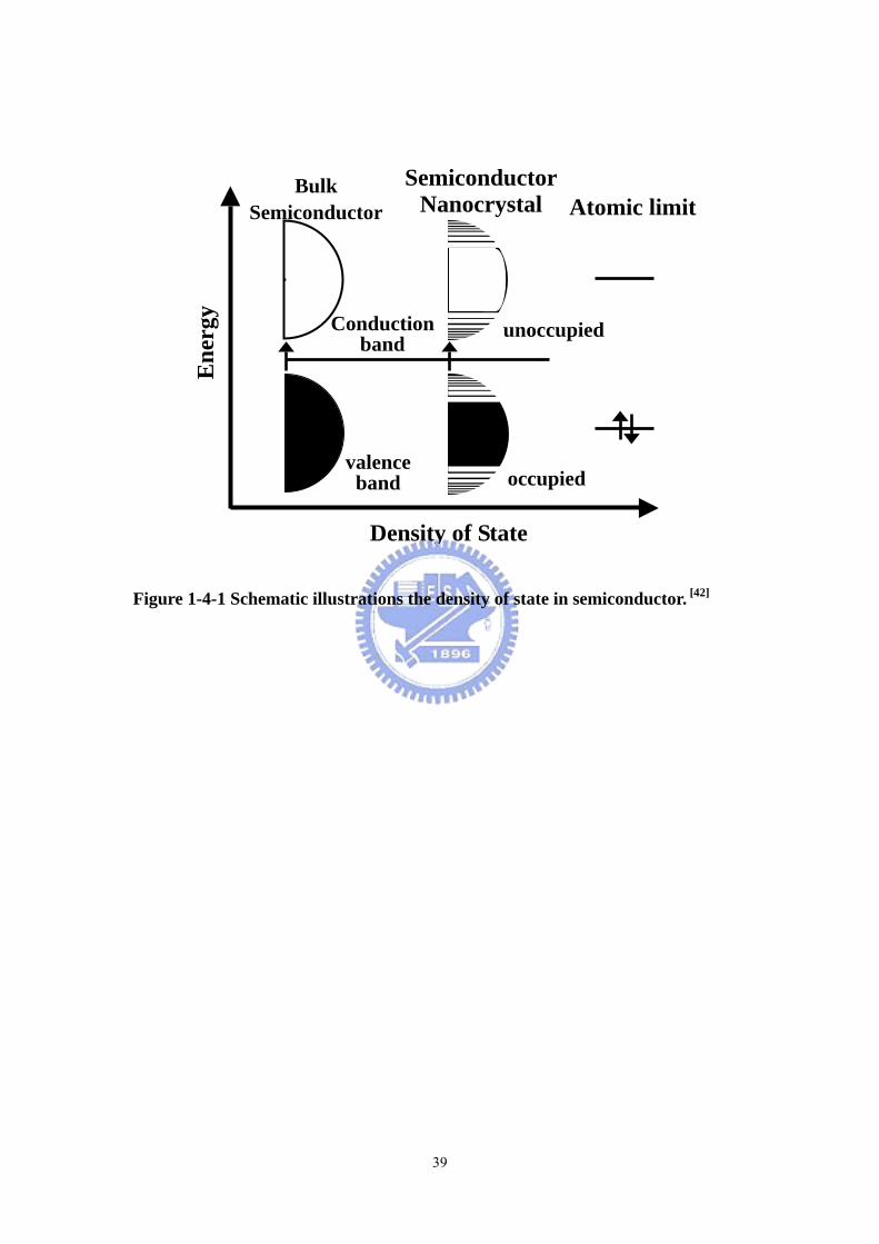
nanostructures. Figure 1-4-1 shows variation of states of electrons with increase the
quantization dimension in quantum structure.
1-2-1 Semiconductor Nanoparticles
Characteristics of Semiconductor Nanoparticles
Semiconductor nanoparticles have an inorganic core that is stabilized by a layer of
surface surfactants. Nanoparticles with a semiconductor as the inorganic
material — so-called quantum dots — exhibit size-tunable band gaps. Shape
control of such colloidally prepared nanostructures has been recently achieved by
modifying the synthesis to obtain rod shaped particles—nanorods.
13
Quantum dots have two obvious characteristics. One is the surface area effect
and the other is quantum confinement effect. In surface area effect, for particles in
such a small size regime, a large percentage of the atom is on or near the surface, for
example, 99% of the atoms are on the surface for a 1nm size particles. [44] The
existence of this vast interface between the nanoparticles and the surrounding medium
can have a profound effect on the particles properties. The imperfect surface of the
nanoparticles may act as electron and/or hole traps upon optical excitation. Thus the
presence of these trapped electrons and holes can in turn modify the optical properties
of the particles. In quantum confinement effect, “confinement” and “quantization”
are two closely related definition: If a particles is “confined” then its energy is
“quantized”, and vice versa. According to the dictionary, to “confine” mean to
“restrict within limits” to “enclose”, and even to “imprison”. The quantum
confinement not only causes the increase of the energy gap (blue shift of the
absorption edge) and the splitting of the electronic states, but also changes the
densities of state and the exciton oscillator strength. [45] It was revealed that many of
the differences between the electronic behaviors of the bulk and the quantum-confined
low-dimensional semiconductors are due to their difference densities of state.
Nanorods exhibit electronic and optical properties that differ from quantum dots.
For example, unlike the spherical dots, nanorods demonstrate linearly polarized
emission [46, 47] leading also to polarized lasing. [48] In addition to size and shape,
nanocrystals’ charging may also significantly influence their electrical and optical
properties. Millo et al. reported optical and tunneling spectroscopies on CdSe
nanorods and correlated the experimental data with the level structure calculated
using a multi-band effective-mass model for an infinite potential well. [49] However,
the experimental set-up in both optical and tunneling measurements was tuned so as
to avoid nanorods charging.
14
Applications of CdSe Nanoparticles
In 1993, a paper entitled “Synthesis and Characterization of Nearly Monodisperse
CdX (X=S, Se, Te) Semiconductor Nanoparticles” by Murray, Norris, and Bawendi
appeared in the Journal ofthe American Chemical Society. [50] CdSe nanoparticles
are (potential) building blocks for new electronic and optical nanodevices such as
light-emitting diodes, solar cells, lasers, and biological labels.
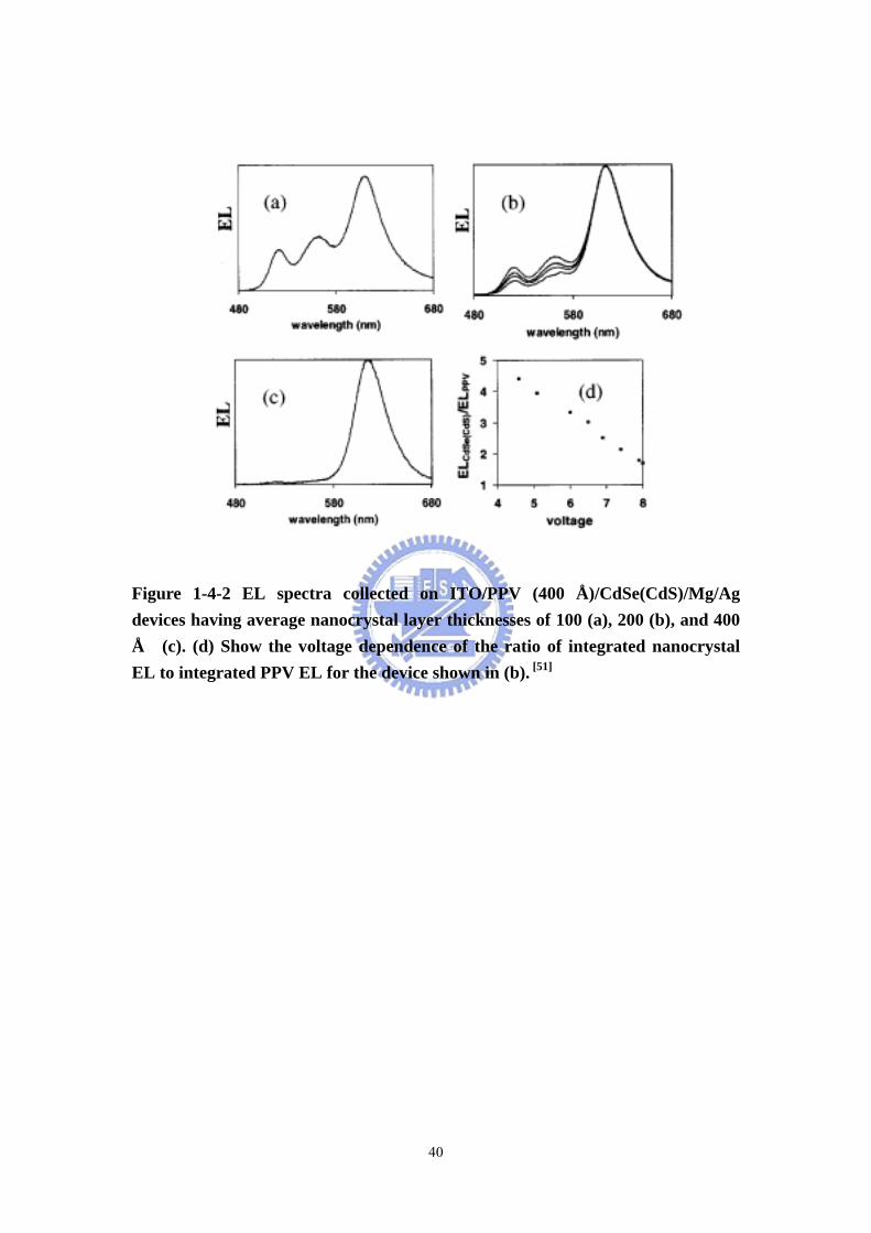
Light-emitting diodes Alivisatos et al. reported improved efficiencies in light
emitting diodes made with CdSe (CdS) core/shell type nanoparticles and a
semiconducting polymer. [51] They reported experiments on bilayer light emitting
diodes made with organically capped CdSe(CdS) core/shell type semiconductor
nanoparticles and an electroluminescent (EL) semiconducting polymer
poly(p-phenylenevinylene) (PPV). The devices emit from red to green with external
quantum efficiencies of up to 0.22% at brightnesses of 600 cd/m2 and current
densities of 1 A/cm2. They have operating voltages as low as 4 V and lifetimes
under constant current flow of hundreds of hours. Most of these numbers are
significant improvements over similar devices made with CdSe nanoparticles. The
devices show either nanoparticle-only EL or a combination of nanoparticle and PPV
EL, depending on nanoparticle layer thickness. The nanoparticle EL is dependent on
nanoparticle size. Some devices show a voltage dependent spectral output. The
spectral output is consistent with a field dependent electron range in the nanoparticle
layer limited by carrier trapping (Figure 1-4-2).
Solar cells Alivisatos et al. reported hybrid CdSe nanorods-conjugated polymer
solar cells. [52] They demonstrated that semiconductor nanorods can be used to
fabricate readily processed and efficient hybrid solar cells together with polymers.
By controlling nanorod length, we can change the distance on which electrons are
transported directly through the thin film device. Tuning the band gap by altering

15
the nanorod radius enabled us to optimize the overlap between the absorption
spectrum of the cell and the solar emission spectrum. A photovoltaic device
consisting of 7-nanometer by 60-nanometer CdSe nanorods and the conjugated
polymer poly-3(hexylthiophene) was assembled from solution with an external
quantum efficiency of over 54% and a monochromatic power conversion efficiency of
6.9% under 0.1 milliwatt per square centimeter illumination at 515 nanometers.
Under Air Mass (A.M.) 1.5 Global solar conditions, we obtained a power conversion
efficiency of 1.7% (Figure 1-4-3).
Lasers Bawendi et al. reported optical gain and stimulated emission in
semiconductor nanoparticles. [53] The development of optical gain in chemically
synthesized semiconductor nanoparticles has been intensely studied as the first step
toward semiconductor nanoparticles lasers. They examined the competing
dynamical processes involved in optical amplification and lasing in semiconductor
nanoparticles and found that, despite a highly efficient intrinsic nonradiative Auger
recombination, large optical gain can be developed at the wavelength of the emitting
transition for close-packed solids of these nanoparticles. Narrowband stimulated
emission with a pronounced gain threshold at wavelengths tunable with the size of the
semiconductor nanoparticle was observed, as expected from quantum confinement
effects. These results unambiguously demonstrate the feasibility of nanocrystal
quantum dot lasers.
Biological labels Alivisatos et al. reported semiconductor nanoparticles as
fluorescent biological labels. [54] Semiconductor nanoparticles were prepared for use
as fluorescent probes in biological staining and diagnostics. Compared with
conventional fluorophores, the nanoparticles have a narrow, tunable, symmetric
emission spectrum and are photochemically stable. The advantages of the broad,
continuous excitation spectrum were demonstrated in a dual-emission,
16
single-excitation labeling experiment on mouse fibroblasts. These nanoparticle
probes are thus complementary and in some cases may be superior to existing
fluorophores.
1-2-2 Metal Nanoparticles
Characteristics of Metal Nanoparticles
Physicists predicted that metal nanoparticles in the diameter range 1-10 nm
(intermediate between the size of small molecules and that of bulk metal) would
display electronic structures, reflecting the electronic band structure of the
nanoparticles, owing to quantum-mechanical rules. [55] The resulting physical
properties are neither those of bulk metal nor those of molecular compounds, but they
strongly depend on the particle size, interparticle distance, nature of the protecting
organic shell, and shape of the nanoparticles. [56] The few “last metallic electrons”
are used for tunneling processes between neighboring particles, an effect that can be
detected by impedance measurements that distinguish intra- and intermolecular
processes.
The quantum size effect is involved when the de Broglie wavelength of the
valence electrons is of the same order as the size of the particle itself. Then, the
particles behave electronically as zero-dimensional quantum dots (or quantum boxes)
relevant to quantum-mechanical rules. Freely mobile electrons are trapped in such
metal boxes and show a characteristic collective oscillation frequency of the plasma
resonance, giving rise to the so-called plasmon resonance band (PRB) observed near
530 nm in the 5-20-nm-diameter range. In nanoparticles, there is a gap between the
valence band and the conduction band, unlike in bulk metals. The size induced
metal-insulator transition, described in 1988, is observed if the metal particle is small
enough (about 20 nm) that size-dependent quantization effects occur. Then,
standing electron waves with discrete energy levels are formed. Single-electron
17
transitions occur between a tip and a nanoparticle, causing the observation of
so-called Coulomb blockades if the electrostatic energy, Ea = e2/2C, is larger than the
thermal energy, ET = kT. The capacitance C becomes smaller with smaller particles.
This means that single-electron transitions can be observed at a given temperature
only if C is very small, i.e., for nanoparticles since they are small enough (C < 10-18 F).
Large variations of electrical and optical properties are observed when the energy
level spacing exceeds the temperature, and this flexibility is of great practical interest
for applications (transistors, switches, electrometers, oscillators, biosensors, catalysis).
[57]
Applications of Au Nanoparticles
Au nanoparticles are the most stable metal nanoparticles, and they present
fascinating aspects such as their assembly of multiple types involving materials
science, the behavior of the individual particles, size-related electronic, magnetic and
optical properties (quantum size effect), and their applications to catalysis and biology.
Their promises are in these fields as well as in the bottom-up approach of
nanotechnology, and they will be key materials and building block in the 21st century.
Memory cells Yang et al. reported electric-field-induced charge transfer between
Au nanoparticles and capping 2-naphthalenethiol and organic memory cells. [58] An
electrical transition, induced by a high electric field, was observed in a device
consisting of a polystyrene film containing 2-naphthalenethiol-capped Au
nanoparticles sandwiched between two Al electrodes. The current through the
device changed from a charge-injection-controlled current to a space-charge-limited
current. The latter current is higher than the former by more than three orders of
magnitude at 2 V. Asymmetrical current-voltage curve was observed along the two
polarity directions for the device after the transition. This transition is attributed to
an electric-field-induced charge transfer between the Au nanoparticle and the capping
18
2-naphthalenethiol. The device exhibits good stability in the high conductivity state,
so it can be used as a write-once-read-many times (Figure 1-4-4).
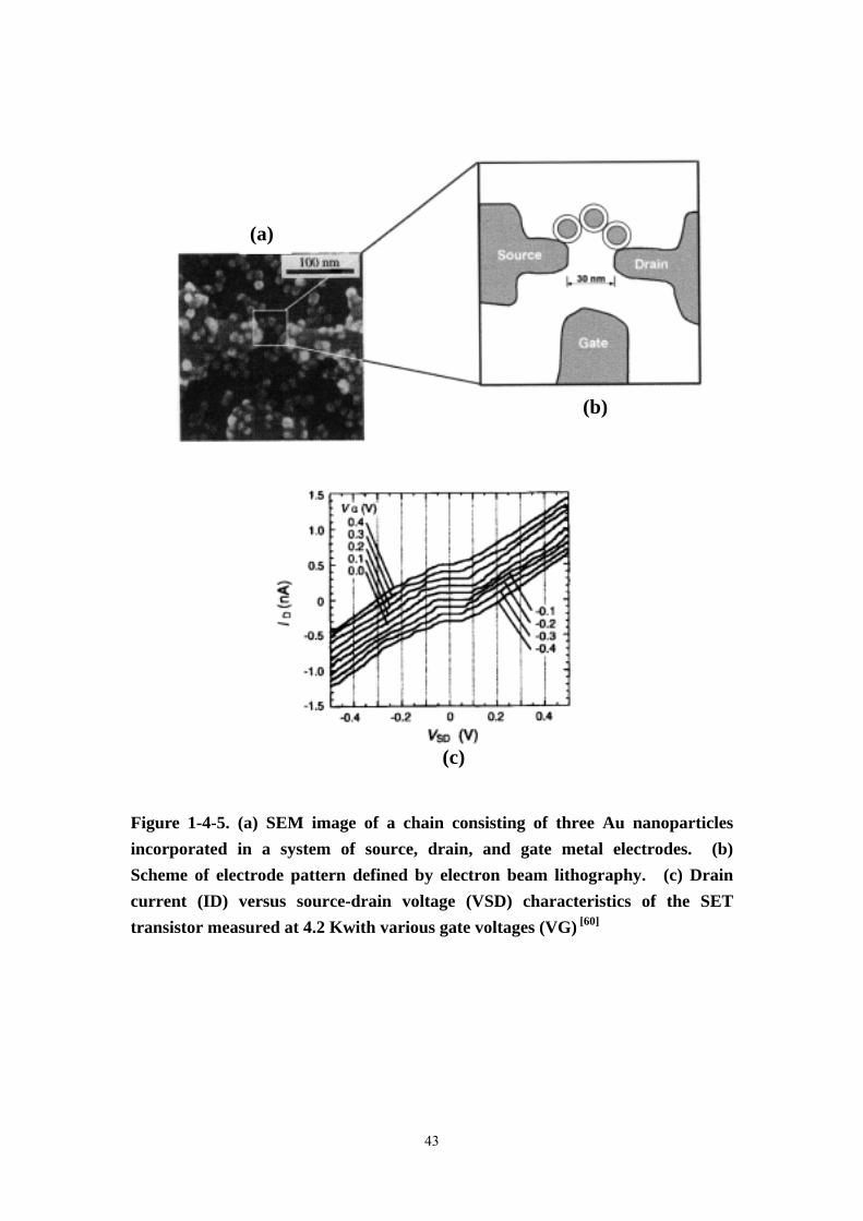
Single-electron transistors Simon reported single electron tunneling in Au
nanoparticle arrangements. [59] Coulomb charging of chemically prepared
nanoparticles has already been utilized to build up “single electron tunneling” (SET)
transistors. Sato et al. [60] reported the electrical characteristics of a SET transistor,
where single 1,6-hexanedithiol-stabilized 10 nm Au nanoparticles were attached by
self-assembly to 3-(2-aminoethylamino) propyltrimethoxysilane-functionalized metal
electrodes, fabricated by electron beam lithography (Figure 1-4-5). Since not all
steps of this procedure could be controlled in detail, the number of nanoparticles in
the chain bridging the 30 nm gap between electrodes differed from device to device.
Up to 77 K conduction was dominated by single electron charging. The capacitance
of all junctions in the chain turned out to be 1.8-2 × 10-18 F and the Coulomb gap
calculated from this value was in reasonable agreement with the value of 150 mV
obtained from the I (U) characteristics. The latter was systematically squeezed,
when a gate voltage of -0.4 to 0.4 V was applied, which reflects the desired function
of the single electron transistor.
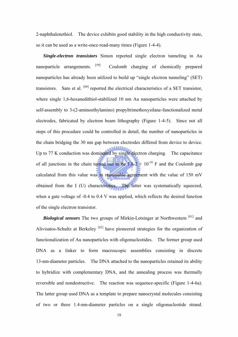
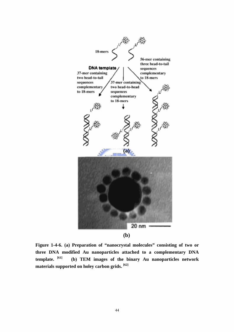
Biological sensors The two groups of Mirkin-Letsinger at Northwestern [61] and
Alivisatos-Schultz at Berkeley [62] have pioneered strategies for the organization of
functionalization of Au nanoparticles with oligonucleotides. The former group used
DNA as a linker to form macroscopic assemblies consisting in discrete
13-nm-diameter particles. The DNA attached to the nanoparticles retained its ability
to hybridize with complementary DNA, and the annealing process was thermally
reversible and nondestructive. The reaction was sequence-specific (Figure 1-4-6a).
The latter group used DNA as a template to prepare nanocrystal molecules consisting
of two or three 1.4-nm-diameter particles on a single oligonucleotide strand.
19
DNA-driven assemblies of Au nanoparticles have indeed attracted considerable
interest, and a new colorimetric technique based on the sensitivity of the SPB to
monitor DNA modification was designed by the Mirkin-Letsinger group. In this
strategy, Au nanoparticles are used as building blocks, allowing the assembly of
alkanethiol-capped oligonucleotides such as single-stranded DNA and complementary
linker oligonucleotide (DNA) strands (Figure 1-4-6b).
Catalysts Au is very popular for being chemically inert. It is indeed one of the
most stable metals in the group 8 elements, and it is resistant to oxidation. In the
1970s, however, Parravano’s group reported the investigation of the activity of Au in
oxygen/hydrogentransfer reactions [63] and the reduction of NO by dihydrogen, but
these studies remained isolated. Therefore, the discovery by Haruta et al., reported
in 1989, that Au nanoparticles supported on Co3O4, Fe2O3, or TiO2 were highly active
catalysts, under high dispersion, for CO and H2 oxidation, NO reduction, water-gas
shift reaction, CO2 hydrogenation, and catalytic combustion of methanol was a
surprise, and was considered important by the chemical community. Catalysis with
Au nanoparticles, in particular the very active oxide-supported ones, is now an
expanding area, and a large number of new catalytic systems for various reactions are
now being explored.
1-2-3 Electrical Properties of Two- and Three-Dimensional
Arrangements of Nanoparticles
Generally speaking, the nanoparticles thin films and similar assemblies can be
classified into three categories: three-dimensional (3D), two-dimensional (2D), and
one-dimensional (1D) systems. 2D and 3D nanoparticle assemblies have been made
by many research groups, by using a large variety of techniques, such as solvent
evaporation, Langmuir-Blodgett transfer, producing self-assembled monolayers and

20
multilayers, and layer-by-layer assembly. In comparison, anisotropic 1D assemblies
of nanoparticles are seldom reported due to the difficulties arising with their
preparation, which stem from the perception of the isotropic structure and
morphology of 0D nanoparticles.
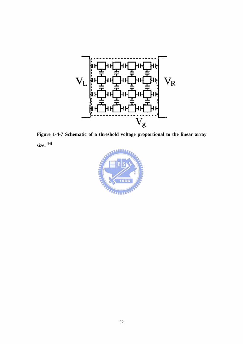
In 1993, Middleton and Wingreen reported collective transport in arrays of small
metallic dots. [64] They examine the low-temperature, non-linear charge transport in
such an array. The dots are treated as capacitively coupled conductors with charges
allowed to tunnel between neighboring dots. In contrast with previous work, [65]
they explicitly include the effects of random offset charges on each dot and
investigate the limit where the number of dots becomes large. They find that the
onset of conduction occurs at a voltage VT proportional to the linear array size (Figure
1-4-7). This sharp onset is to be contrasted with conduction in one- and
two-dimensional disordered materials, where an increasing electric field leads to a
smooth increase in conductivity. One of the correlation lengths that diverges near
this threshold is found from a general argument based on interface growth, while
anther is found by focusing on “slow points” which control the current. These
correlation lengths determine the branching of current paths in the array and hence the
current near onset. In particular, they predict that the current through linear and
square arrays behaves as
ζ
−∝ 1
TVVI ………(1-1)
with ζ=1, 5/3 in dimensionsd=1, 2, respectively.
Three-dimensional arrangements Brinker et al. reported self-assembly of ordered,
robust, three-dimensional gold nanoparticle/silica arrays. [66] They reported the
synthesis of a new nanoparticle mesophase through selfassembly of water-soluble
nanoparticle micelles with soluble silica. The mesophase comprises Au nanoparticles
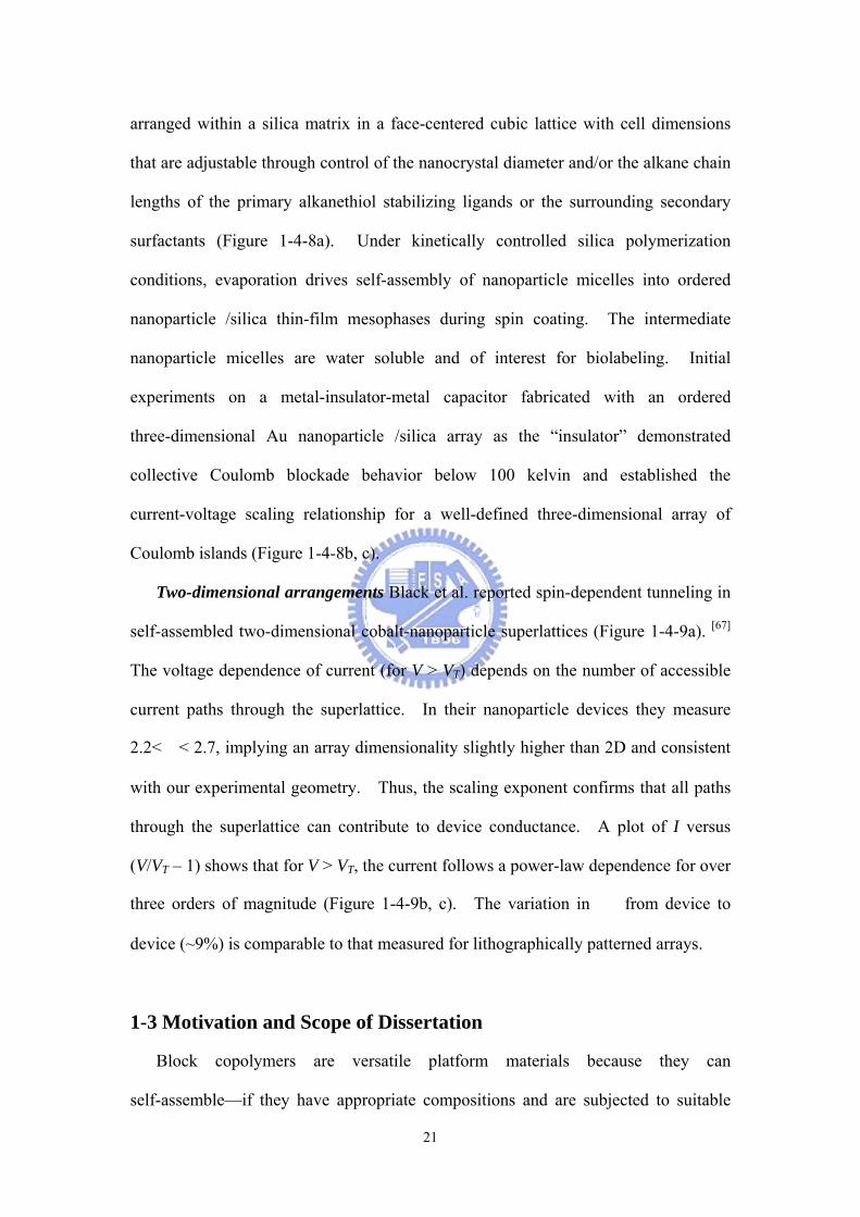
21
arranged within a silica matrix in a face-centered cubic lattice with cell dimensions
that are adjustable through control of the nanocrystal diameter and/or the alkane chain
lengths of the primary alkanethiol stabilizing ligands or the surrounding secondary
surfactants (Figure 1-4-8a). Under kinetically controlled silica polymerization
conditions, evaporation drives self-assembly of nanoparticle micelles into ordered
nanoparticle /silica thin-film mesophases during spin coating. The intermediate
nanoparticle micelles are water soluble and of interest for biolabeling. Initial
experiments on a metal-insulator-metal capacitor fabricated with an ordered
three-dimensional Au nanoparticle /silica array as the “insulator” demonstrated
collective Coulomb blockade behavior below 100 kelvin and established the
current-voltage scaling relationship for a well-defined three-dimensional array of
Coulomb islands (Figure 1-4-8b, c).
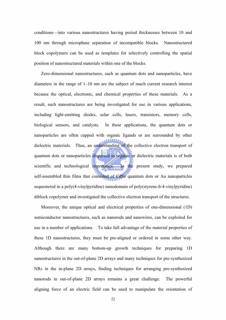
Two-dimensional arrangements Black et al. reported spin-dependent tunneling in
self-assembled two-dimensional cobalt-nanoparticle superlattices (Figure 1-4-9a). [67]
The voltage dependence of current (for V > VT) depends on the number of accessible
current paths through the superlattice. In their nanoparticle devices they measure
2.2<ζ< 2.7, implying an array dimensionality slightly higher than 2D and consistent
with our experimental geometry. Thus, the scaling exponent confirms that all paths
through the superlattice can contribute to device conductance. A plot of I versus
(V/VT – 1) shows that for V > VT, the current follows a power-law dependence for over
three orders of magnitude (Figure 1-4-9b, c). The variation in ζ from device to
device (~9%) is comparable to that measured for lithographically patterned arrays.
1-3 Motivation and Scope of Dissertation
Block copolymers are versatile platform materials because they can
self-assemble—if they have appropriate compositions and are subjected to suitable
22
conditions—into various nanostructures having period thicknesses between 10 and
100 nm through microphase separation of incompatible blocks. Nanostructured
block copolymers can be used as templates for selectively controlling the spatial
position of nanostructured materials within one of the blocks.
Zero-dimensional nanostructures, such as quantum dots and nanoparticles, have
diameters in the range of 1–10 nm are the subject of much current research interest
because the optical, electronic, and chemical properties of these materials. As a
result, such nanostructures are being investigated for use in various applications,
including light-emitting diodes, solar cells, lasers, transistors, memory cells,
biological sensors, and catalysts. In these applications, the quantum dots or
nanoparticles are often capped with organic ligands or are surrounded by other
dielectric materials. Thus, an understanding of the collective electron transport of
quantum dots or nanoparticles dispersed in organic or dielectric materials is of both
scientific and technological importance. In the present study, we prepared
self-assembled thin films that consisted of CdSe quantum dots or Au nanoparticles
sequestered in a poly(4-vinylpyridine) nanodomain of poly(styrene-b-4-vinylpyridine)
diblock copolymer and investigated the collective electron transport of the structures.
Moreover, the unique optical and electrical properties of one-dimensional (1D)
semiconductor nanostructures, such as nanorods and nanowires, can be exploited for
use in a number of applications. To take full advantage of the material properties of
these 1D nanostructures, they must be pre-aligned or ordered in some other way.
Although there are many bottom-up growth techniques for preparing 1D
nanostructures in the out-of-plane 2D arrays and many techniques for pre-synthesized
NRs in the in-plane 2D arrays, finding techniques for arranging pre-synthesized
nanorods in out-of-plane 2D arrays remains a great challenge. The powerful
aligning force of an electric field can be used to manipulate the orientation of

23
anisotropic materials by taking advantage of their different anisotropic dielectric
constants. In this thesis, we applied an electric field to induce the orientation of
CdSe nanorods that had been self-assembled in the poly(4-vinylpyridine)
nanodomains of a poly(styrene-b-4-vinylpyridine) diblock copolymer thin film.

24
Figure 1-1-1 Schematic phase diagram showing the various ‘classical’ block copolymer morphologies adopted by linear diblock copolymer. [6]
25
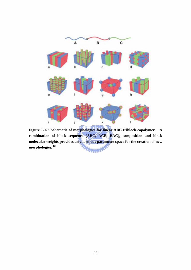
Figure 1-1-2 Schematic of morphologies for linear ABC triblock copolymer. A combination of block sequence (ABC, ACB, BAC), composition and block molecular weights provides an enormous parameter space for the creation of new morphologies. [6]

26
Figure 1-2-1 The well-known structures of block copolymers in melt, solution or solid state. [8]
27
Figure 1-3-1 Schematic of various applications of block copolymers in nanotechnologies. [9]
Block Copolymer Nanotechnology
photonic crystal
waveguide
tunable photonic crystal
nanomask
nanotemplate
nanowire
transistor
patterned media
ceramic membrane
28
Figure 1-3-2 Schematic of the production process of a metal nanodot array using block copolymer lithography. [12]
29
Figure 1-3-3 SEM image of polystyrene-b-polyferrocenyldimethylsilane mask, after the polystyrene has been removed by O2 RIE. [14]
30
Figure 1-3-4 Schematic representation of high density nanowire fabrication in a polystyrene-b-poly(methylmethacrylate) matrix. [15]
31
Figure 1-3-5 The morphological transformation from a hexagonally packed cylinder structure of pure polystyrene-b-poly(4-vinylpyridine) (PS-b-P4VP) diblock copolymers to lamellar (CdS/P4VP)-b-PS composites. [18]
without CdS low (7% inP4VP) high (28% inP4VP)
CdS content in PS-b-P4VP diblock copolymers
P4VP
PS PS
CdS/P4VP CdS
HEX Lamellar Destroyed lamellar
CdS/P4VP
PS

32
Figure 1-3-6 Schematic of selectived distribution of TiO2 nanoparticles in polystyrene-b-poly(methylmethacrylate) diblock copolymer. [19]
PS-b-PMMA
N
N
N
N
NNN
NNN
NN
N N NN
N
N
NN
NN
N
NN N
N
N
NN
solvent removal
TiO2-TMAC (ionic surfactant)
TiO2-TMAC aggregates in PS domain
(a)
(b)
solvent removal
TiO2-TMS (covalently-bond
ed surfactant)
TiO2-TMS disperses well in PMMA domain
33
Figure 1-3-7 (a) Secondary electron SEM image of the surface of a thin film of a diblock copolymer–CdSe nanoparticle mixture spin-coated onto a silicon wafer and annealed at 170 ℃ for 2 days (image width, 250 nm) taken at 1-kV acceleration voltage. (b) Schematic representation of nanoparticle assembly at the poly(2-vinylpyridine) cylinders. [25]
(a)
(b)
34
Figure 1-3-8 TEM micrograph of a ternary blend of polystyrene-b-poly(ethylene propylene) + AuR1 + SiO2R2 with inorganic filling fraction f = 0:02; respectively, after micro-sectioning normal to the layer direction (no stain). [26] (AuR1 is Au-S-C18H37and SiO2R2 is SiO2-(Si(CH3)3)2)
35
Figure 1-3-9 (a) Assembly of Au nanoparticles (core: 3.9 ± 1.0 nm; shell: polystyrene; (core+shell)=7.7 nm) into polystyrene-b-poly(2-vinylpyridine) diblock copolymers. (b) Assembly of Au nanoparticles (core: 3.9 ± 1.0 nm; shell: polystyrene and poly(2-vinylpyridine); (core+shell)=7.7 nm) into polystyrene-b-poly(2-vinylpyridine) diblock copolymers. (c), (d) The respective histograms of particle locations for the samples shown in (a) and (b). Reprinted with permission. [27]
(a) (c)
(b) (d)
36
Figure 1-3-10 Cross-sectional transmission electron micrograph showing Au nanoparticles patterned within the poly(4-vinylpyridine) lamellae formed by a polystyrene-b-poly(4-vinylpyridine) diblock copolymer. [34]
37
Figure 1-3-11 Schematic of synthesis of needle-like TiO2 nanostructures with ordered patterns. [36]
Dip in Ti precursor solution
At 60℃
PS-b-P4VP
Ti(OH)22+
Ti(OH)22+ in PS-b-P4VP
micelles
After O2 plasma process
anneal at 170℃in vacuum
TiO2 seeds
~50nm ~120nm ~65nm
80nm
(a)
150 nm
(b)
38
Figure 1-3-12 SEM image of an etched polystyrene-b-polyisoprene diblock, showing a fracture surface. The polystyrene network channels remaining after removal of polyisoprene are clearly visible. [39]
39
Figure 1-4-1 Schematic illustrations the density of state in semiconductor. [42]
Atomic limit Bulk
SemiconductorSemiconductor
Nanocrystal
Conductionband
valenceband
unoccupied
occupied
Density of State
Ene
rgy
40
Figure 1-4-2 EL spectra collected on ITO/PPV (400 Å)/CdSe(CdS)/Mg/Ag devices having average nanocrystal layer thicknesses of 100 (a), 200 (b), and 400 Å (c). (d) Show the voltage dependence of the ratio of integrated nanocrystal EL to integrated PPV EL for the device shown in (b). [51]
41
Figure 1-4-3 (a) The structure of regioregular P3HT. (b) The schematic energy level diagram for CdSe nanorods and P3HT showing the charge transfer of electrons to CdSe and holes to P3HT. (c) The device structure consists of a film ;200 nm in thickness sandwiched between an aluminum electrode and a transparent conducting electrode of PEDOT:PSS. [52]

42
Figure 1-4-4. I-V curve of Al/Au-2NT NPs+PS/ Al. The arrows indicate the biasscanning directions and the inset the device structure. [58]
43
Figure 1-4-5. (a) SEM image of a chain consisting of three Au nanoparticles incorporated in a system of source, drain, and gate metal electrodes. (b) Scheme of electrode pattern defined by electron beam lithography. (c) Drain current (ID) versus source-drain voltage (VSD) characteristics of the SET transistor measured at 4.2 Kwith various gate voltages (VG) [60]
(a)
(b)
(c)
44
Figure 1-4-6. (a) Preparation of “nanocrystal molecules” consisting of two or three DNA modified Au nanoparticles attached to a complementary DNA template. [61] (b) TEM images of the binary Au nanoparticles network materials supported on holey carbon grids. [62]
(a)
(b)
45
Figure 1-4-7 Schematic of a threshold voltage proportional to the linear array
size. [64]

46
Figure 1-4-8 (a) Representative TEM images of Au nanoparticles /silica mesophases. (b) I-V curves measured from 300 K to 78 K. The inset plots the zero-bias conductance (G0) versus 1/T. (c) At T = 78 K, current displays a power-law dependence for V > VT with scaling exponent ζ= 2.7 (negative bias) andζ= 3.0 (positive bias). [66]
(a)
(b)
(c)

47
Figure 1-4-9 (a) SEM image of self-assembled Co nanoparticles superlattice device (b) Device I-V characteristic, for T= 2 K (dark line) and 20, 40, and 70 K (light lines). (Inset) Plot of zero-bias conductance versus 1/T. (c) For V > VT, current displays a power-law dependence. [67]
(a)
(b)
(c)
48
Chapter 2: Basic Electron Transport Theory
2-1 Introduction
To understand the electrical conduction of a metal-molecule system, the energy
level matching (or mismatching) of the available electrons in the metal (the Fermi
level) and the available molecular orbital in the terminal molecule must be considered.
In general, the Fermi level of the metallic contact does not energetically line up with
either the HOMO or LUMO levels in the molecule. [68] This mismatch gives rise to a
contact barrier, analogous to a Schottky contact. Electron (or hole) transport through
such a contact will exhibit a range of phenomena, depending on the height of the
barrier, the effective barrier thickness, and the presence of defects; the most prevalent
are thermionic emission, direct tunneling, and defectmediated transport such as
hopping. [69]
2-2 Conduction Mechanisms
Table 1 lists the possible conduction mechanisms with their characteristic
behavior, temperature dependence, voltage dependence, and schematic band diagrams.
Schottky emission is a process in which carriers overcome the metal-dielectric barrier
by thermionic emission, whose current is a strong function of temperature. The
extra voltage term on the exponential lowers the barrier at the metal-insulator
interface due to image-force correction. Frenkel-Poole (FP) conduction is due to
field-enhanced thermal excitation of trapped electrons into the conduction band, a
process similar to Schottky emission. Instead of the metal-dielectric barrier height
found in Schottky emission, the barrier height in FP conduction represents the depth
of the trap potential with respect to the edge of the conduction band. Its current has
the same temperature dependence as that of Schottky emission, but with different
voltage dependence. As seen from its characteristics, the barrier lowering is twice
49
that observed in Schottky emission, because of the immobility of the positive charge
associated with the trap. Hopping conduction refers to the process in which
thermally excited electrons hop from one isolated state to the next, whose
conductance also depends strongly on temperature. Different from Schottky
emission, there is no barrier lowering effect. The tunneling processes (both Fowler
Nordheim tunneling and direct tunneling) do not depend on temperature (to first
order), but strongly depend on film thickness and voltage. For a given
metal-dielectric film-metal system, certain conduction mechanisms may dominate in
certain voltage and temperature regimes. For example, Schottky emission usually
plays an important role at high temperatures and low barrier heights; Frenkel-Poole
conduction will dominate if there is a high density of traps in the dielectrics; tunneling
current will be a major contribution if the dielectrics is thin and under high voltage
biases; and for a dielectric film that has a very low density of thermally generated free
carriers in the conduction band, hopping conduction is more likely to be observed,
especially at low applied voltages and high temperatures.
2-3 Alkanethiol Self-assembled Monolayers (SAMs)
Metal-Insulator-Metal Tunneling
When the molecular layer is a large bandgap insulator, well-defined
metal-insulator-metal (MIM) tunneling should occur. Temperature-independent
electron transport due to direct tunneling should be the dominant conduction
mechanism. Other mechanisms will be discussed in further sections; however, a
MIM signature is important to determine if the transport is determined by the band
structure of the molecular layer, or due to other less intrinsic effects. An
investigation of these systems has been done, [70,71] specifically alkanethiol
[CH3(CH2)n-1SH] because it forms a robust SAM on Au surfaces. A few groups
have utilized the scanning tunneling microscope, [73] the conducting atomic force
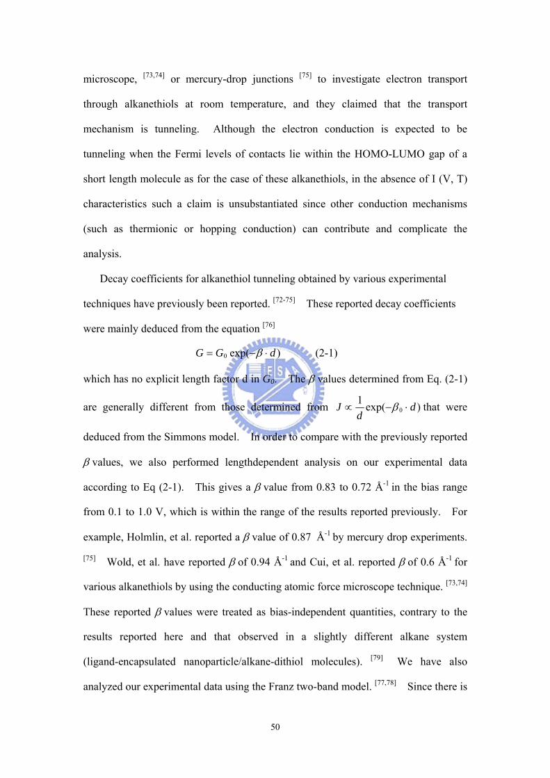
50
microscope, [73,74] or mercury-drop junctions [75] to investigate electron transport
through alkanethiols at room temperature, and they claimed that the transport
mechanism is tunneling. Although the electron conduction is expected to be
tunneling when the Fermi levels of contacts lie within the HOMO-LUMO gap of a
short length molecule as for the case of these alkanethiols, in the absence of I (V, T)
characteristics such a claim is unsubstantiated since other conduction mechanisms
(such as thermionic or hopping conduction) can contribute and complicate the
analysis.
Decay coefficients for alkanethiol tunneling obtained by various experimental
techniques have previously been reported. [72-75] These reported decay coefficients
were mainly deduced from the equation [76]
)exp(0 dGG ⋅−= β (2-1)
which has no explicit length factor d in G0. The β values determined from Eq. (2-1)
are generally different from those determined from )exp(10 d
dJ ⋅−∝ β that were
deduced from the Simmons model. In order to compare with the previously reported
β values, we also performed lengthdependent analysis on our experimental data
according to Eq (2-1). This gives a β value from 0.83 to 0.72 Å-1 in the bias range
from 0.1 to 1.0 V, which is within the range of the results reported previously. For
example, Holmlin, et al. reported a β value of 0.87 Å-1 by mercury drop experiments.
[75] Wold, et al. have reported β of 0.94 Å-1 and Cui, et al. reported β of 0.6 Å-1 for
various alkanethiols by using the conducting atomic force microscope technique. [73,74]
These reported β values were treated as bias-independent quantities, contrary to the
results reported here and that observed in a slightly different alkane system
(ligand-encapsulated nanoparticle/alkane-dithiol molecules). [79] We have also
analyzed our experimental data using the Franz two-band model. [77,78] Since there is
51
no reliable experimental data on the Fermi level alignment in these metal-SAM-metal
systems, ΦB and m* are treated as adjustable parameters. We performed least square
fitting on our data with the Franz nonparabolic E-k relationship using the alkanethiol
HOMO-LUMO gap of 8 eV. [80,81] Figure 2-1 shows the resultant E-k relationship
(following references [77,78]) and the corresponding energy band diagrams. The best
fitting parameters by minimized χ2 were obtained as ΦB = 1.39 eV and m* = 0.45 m.
Both electron tunneling around LUMO and hole tunneling around HOMO in the
forbidden gap can be described by these parameters. ΦB = 1.39 eV indicates that the
Fermi levels are aligned close to one band in either case, therefore the Simmons
model is a valid approximation. The previous best fits obtained from the Simmons
model of ΦB = 1.40 eV and α = 0.65 (corresponding to m* = 0.42 m for the
rectangular barrier case) are in excellent agreement.

52
Table 2-1: Possible conduction mechanisms.
53
Figure 2-1: E-k relationship (symbols) generated from the length-dependent measurement data for alkanethiols. Solid and open symbols correspond to electron and hole tunnelings, respectively. The insets show the corresponding energy band diagrams. The solid curve is the Franz two-band expression for m* = 0.45 m.
54
Chapter 3: Enhanced Collective Electron Transport by CdSe
Quantum Dots Self-Assembled in the Poly(4-vinylpyridine)
Nanodomains of a Poly(styrene-b-4-vinylpyridine) Diblock
Copolymer Thin Film
3-1 Introduction
For semiconductor nanoparticles (NPs), quantum dots (QDs), that have sizes close
to their Bohr exciton radius (typically between 1 and 10 nm), their size-dependent
band gaps result in tunable optical properties. [82] As a result, they possess a wide
range of electrical and optical properties and can be used for various applications,
such as light-emitting diodes, solar cells, lasers, and transistors. In these applications,
composite materials involving nanoparticles and other organic materials were often
adopted. Thus, an understanding of the collective electron transport of QDs
dispersed in the organic materials is of both scientific and technological importance.
A number of reports have described the three- and two-dimensional electron transport
in ordered arrays of Au NPs/SiO2 superlattices, [83] ZnO QDs assemblies, [84] and
organically capped CdSe QDs.[85] In addition, electron transport also has been
examined in granular films of Au NPs linked by alkanethiol molecules[86] or
poly(4-vinylpyridine)[87] and Au/spacer/CdSe QD[88] assemblies. Orbital-selective
electron transport through a single CdSe QD measured with an STM has also been
reported. [89]
Thin films of diblock copolymers are versatile templates for the preparation of
long-range-ordered nanostructures of dots because their periodic thicknesses can be
tuned between 10 and 100 nm. [90] For example, the selective sequestration of
pre-synthesized CdS, [20] CdSe[92] and TiO2[91a] nanoparticles into one block of diblock
copolymers are performed by ensuring the presence of strong interactions between
one block of a diblock copolymer and the surface ligands of the nanoparticles. An

55
assembly of Au nanoparticles enclosed by a block copolymer has also been reported.
[93] In the present study, we prepared self-assembled thin films that consisted of
CdSe QDs sequestered in a poly(4-vinylpyridine) nanodomain of
poly(styrene-b-4-vinylpyridine) (S4VP) diblock copolymer, following a previous
approach. [20,91] By conductive atomic force microscopy (C-AFM) and device
measurements, we found that the electron tunneling rate constant in the case of CdSe
QDs confined in a poly(4-vinylpyridine) nanodomain is much larger than that in the
randomly distributed case. To our knowledge, this is the first time the nanodomain
confined effect on the collective electron transport behavior of quantum dots has been
reported. This work has great implications on hybrid photovoltaic cell or
light-emitting diode applications because collective electron transport by CdSe QDs
and hole transport by organic materials, respectively, are critical for producing highly
efficient hybrid photovoltaic cell [82] or light emitting diode. [94]
3-2 Methods and Analysis
3-2-1 Materials. The poly(styrene-b-4-vinylpyridine) (S4VP) diblock copolymer
and the poly(4-vinylpyridine) homopolymer were purchased from Polymer Source,
Inc. The polydispersity index (Mw/Mn) was 1.23, and the molecular weights (Mn)
of the PS and P4VP blocks were 365,300 and 29,400 g/mol, respectively. Cadmium
oxide (CdO, 99.9%), selenium (Se, 99.9%, 100 mesh), and trioctylphosphine (TOP)
were obtained from Aldrich. Trioctylphosphine oxide (TOPO), 1-octadecene (ODE),
and n-hexadecylamine (HDA) were purchased from Lancaster. Stearic acid (99%,
Avocado), hexane (99%, TEDIA USA), toluene (99%, TEDIA USA), methyl alcohol
(MeOH, 99%, TEDIA USA), and pyridine (99%, Showa) were obtained from
commercial sources.
3-2-2 Synthesis of CdSe/TOPO QDs. CdSe QDs were synthesized using a

56
modification of a procedure reported previously. [100] First, a mixture of CdO (0.2
mmol), stearic acid (0.8 mmol), and ODE (2 g) was heated in a 25 mL three-neck
flask to ca. 200 °C to obtain a colorless, clear solution. After this solution had
cooled to room temperature, HDA (1.5 g) and TOPO (0.5 g) were added to the flask.
This system was then reheated to 280 °C under an argon flow. At this temperature, a
selenium solution, prepared by dissolving Se (2 mmol) in TOP (1 mL), was injected
rapidly. The growth temperature was reduced to 250 °C for 30 s and then the
reaction mixture was cooled to room temperature. The dots were collected as
powders using size-selective precipitation with methanol and then redispersed in
toluene.
3-2-3 Preparation of CdSe/pyridine QDs. CdSe/TOPO powder (30 mg) was
dissolved in pyridine (5 mL) and then stirred at 65 °C for 6 h. Hexane (30 mL) was
added to reprecipitate the CdSe. The orange/red suspension was centrifuged and
then the powder was collected and redissolved in pyridine.
3-2-4 Preparation of bulk (CdSe/P4VP)-b-PS. PS-b-P4VP (0.05 g) was added to
pyridine (1 mL). Samples of 10, 15, 26, 33, and 48% CdSe/pyridine (with respect to
the volume fraction of P4VP block) were mixed in the PS-b-P4VP/pyridine
polymerization solution. These mixtures were dried slowly under vacuum at 50 °C
and then maintained at 160 °C for 48 h to obtain the bulk (CdSe/P4VP)-b-PS
composites.
3-2-5 Preparation of thin films of (CdSe/P4VP)-b-PS. Micellar solutions (0.5 wt%)
of (CdSe/P4VP)-b-PS were prepared by dissolving bulk (CdSe/P4VP)-b-PS in toluene.
The micellar solutions were spin-coated at 5000 rpm for 60sec on carbon-coated
silicon wafers for transmission electron microscopy (TEM), and Pt-coated wafer for
conductance atomic force microscopy (C-AFM) and device measurement. We
prepared the sample of CdSe distributed in P4VP homopolymer under the same
57
conditions we had used to prepare (CdSe/P4VP)-b-PS, including the amount of CdSe
in P4VP and the thickness of the thin CdSe/P4VP film.
3-2-6 Characterization. TEM images were obtained using a JOEL-2010 transmission
electron microscope. The thin film sample for TEM was prepared by using 1% HF
to remove it from the carbon-coated silicon wafer. C-AFM measurements were
performed using a Digital Nanoscope IV3100 under ambient conditions. The
current-voltage (I-V) characteristics of device of thin films of (CdSe/P4VP)-b-PS was
measured by Hewlett-Packard 4156B. Using a base pressure below 1 × 10⁻⁶ Torr, a
layer of Al (100nm) was vacuum deposited as top electrode. UV–Vis absorption
spectra were obtained on an Aglient 8453 spectrometer by scanning between 190 and
1000 nm. Photoluminescence spectra (PL) were obtained at room temperature using
a Hitachi F4500 fluorescence spectrophotometer. The concentrations of the
CdSe/TOPO in toluene and CdSe/pyridine solutions were diluted to 6 × 10⁻⁵ M for the
UV–Vis and PL spectroscopy experiments. Small-angle X-ray scattering
experiments were performed on a wiggler beamline BL-01B1 at the National
Synchrotron Radiation Research Center, Taiwan. The cyclic voltammetry (CV)
curve of pure P4VP was measured by coating the polymer onto a Pt plate and using a
standard calomel electrode as the reference and 0.1 M (n-Bu)4NBF4/acetonitrile as the
electrolyte; the scanning rate was set to 50 mV/sec.
3-3 Results and Discussions
Scheme 3-1 demonstrates the process for preparing a mono-layered
(CdSe/P4VP)-b-PS thin film. First, the TOPO ligands on CdSe QDs were
exchanged by hydrophilic pyridine ligands. Then, pyridine-modified CdSe QDs and
PS-b-P4VP block copolymer are dissolved and mixed in pyridine, and CdSe QDs are
distributed selectively in the P4VP phase due to the dipole-dipole interactions. After
58
drying, (CdSe/P4VP)-b-PS in bulk form was obtained. Subsequently, toluene, which
is a good solvent for PS but a poor one for P4VP, is used to form a solution containing
micelles of CdSe/P4VP-core and PS-shell. Figure 3-1a displays the transmission
electron microscopy (TEM) image of a thin film of 48% (CdSe/P4VP)-b-PS obtained
without staining. The dark region represents the CdSe/P4VP composite phase
(because of the higher electron density of cadmium). The spherical nanostructure of
PS-b-P4VP is, therefore, revealed clearly. The diameter of the CdSe/P4VP sphere
was ca. 35 nm, and the inter-domain distance was ca. 100 nm. The inset of Figure
3-1a reveals that CdSe QDs were dispersed homogeneously in the P4VP nanodomain.
Figure 3-1b displays a schematic representation of the C-AFM method we used to
analyze the CdSe/P4VP spheres embedded in the polystyrene. The current image
was measured at the sample bias of VB = 8 V. Figure 3-1c presents the topographic
and current images of a section of the thin film of 48% (CdSe/P4VP)-b-PS. In the
height image, the light regions having a size of ca. 35 nm represent the CdSe/P4VP
domains, while the dark area represents the polystyrene matrix. Because the
thickness of the thin film is smaller than the size of the CdSe/P4VP domain (23 vs. 30
nm), this image indicates that the microphase-separated (CdSe/P4VP)-b-PS exists as a
monolayered thin film. In the current image, the values of the currents of the
P4VP/CdSe phases (light region) were ca. 30–40 pA, whereas that of the PS phase
(dark region) was at the level of the noise (ca. 0.5 pA).
Figure 3-2a displays the current–voltage (I–V) curves of a single CdSe/P4VP
nanodomain as measured by C-AFM. The turn-on voltages for the CdSe/P4VP
nanodomain decreased as the number of incorporated CdSe QDs increased. This
phenomenon occurs because the electron mobility from the probe to the nanodomain
increased upon increasing the density of the CdSe QDs. The linear regions of the
I-V curves represent the Ohmic behavior, [98] and indicate constant conductivities (σ )
59
that can be calculated from the slope of the curves. [95] The nonlinear regions were
due to the electron tunneling from probe tip to the conduction band of CdSe QDs,
which must overcome the barrier height ( eφ ) of the P4VP between the tip and CdSe
(Inset of Figure 3-2a). [95, 101a] A tunneling process, in which electron injection
occurs under a forward bias, can be properly modeled using the Fowler–Nordheim
(FN) equation. The FN equation can be used to determine the electron barrier height
( eφ ). [95] The eφ values for the 10, 15, 26, 33, and 48% CdSe QDs in the P4VP
block were 2.4, 2.2, 2.0, 1.8, and 1.5 eV, respectively. [95] The electron barrier height
( eφ ) decreases monotonically when the amount of CdSe QDs in the P4VP block
increases, owing to the fact that the distance between tip and CdSe QDs decreased at
higher CdSe QDs densities. Figure 3-2b displays the conductivity of a single
CdSe/P4VP nanodomain plotted against the volume fraction of incorporated CdSe in
P4VP. The conductivity of the CdSe/P4VP nanodomain displays only a slight
change at low CdSe loading, exhibits a sharp increase at a critical loading, and
becomes saturated at high loading. Hence, the conductivity of polymers
incorporating CdSe QDs is best described by a percolation theory (the solid curve in
Figure 3-2b represents the best fit to the experiment data). [95] Table 3-1 lists the
conductivity of a single CdSe/P4VP nanodomain of the samples, σ , as ranging from
10–5 to 10–7 Ω–1cm–1. The conductivity (σ ) increases as the amount of CdSe
increased, owing to the fact that the distance between CdSe QDs decreased at higher
CdSe QDs densities. We also obtained the averaged current–voltage (Iave–V) curves
of a single CdSe/P4VP nanodomain in PS matrix by a sandwiched device. [95] The
conductivity (σ ) also increases as the amount of CdSe increased and is of the same
order of magnitude as compared to that by C-AFM measurement, ranging from 10–5
to 10–7 Ω–1cm–1, given in Table 3-1.
Figure 3-3a displays a plot of –ln (σ ) vs. the edge-to-edge interparticle distance
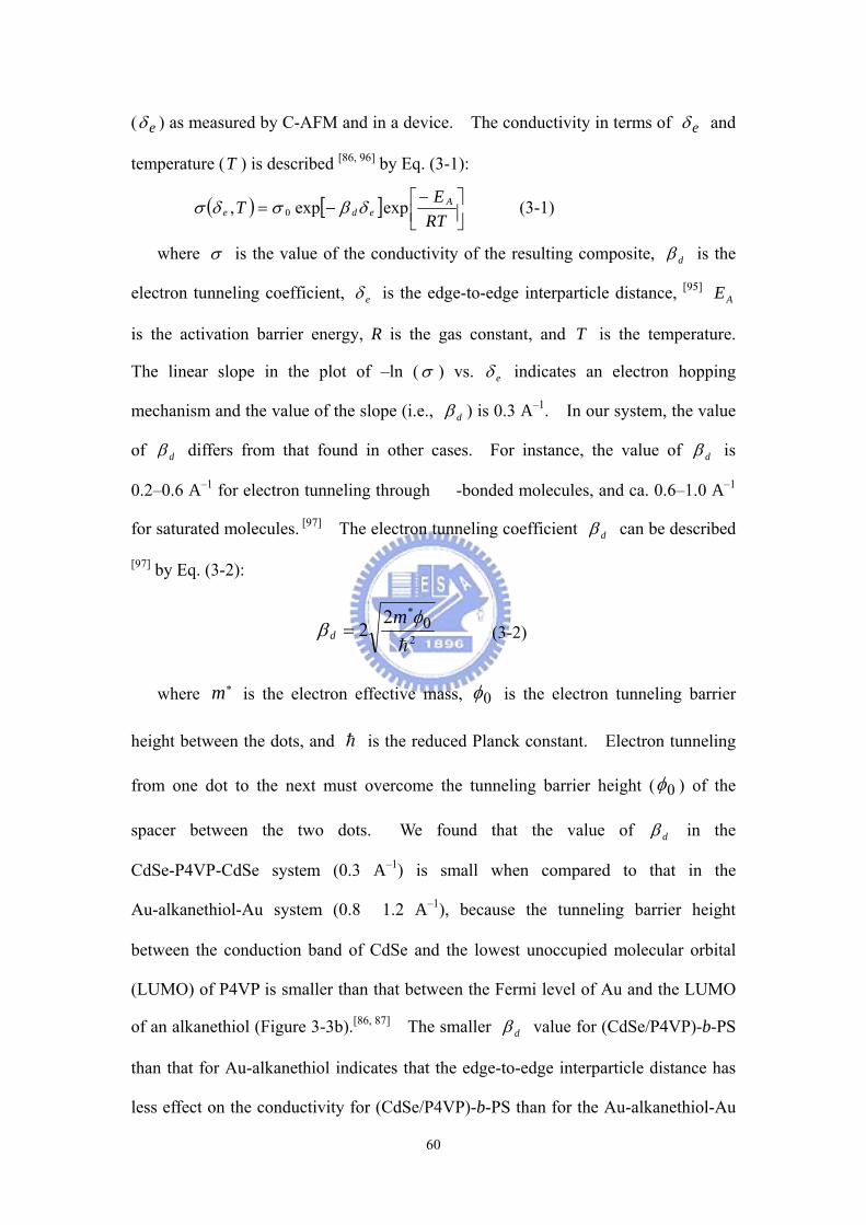
60
( eδ ) as measured by C-AFM and in a device. The conductivity in terms of eδ and
temperature (T ) is described [86, 96] by Eq. (3-1):
( ) [ ]
−
−=RTET A
ede expexp, 0 δβσδσ (3-1)
where σ is the value of the conductivity of the resulting composite, dβ is the
electron tunneling coefficient, eδ is the edge-to-edge interparticle distance, [95] AE
is the activation barrier energy, R is the gas constant, and T is the temperature.
The linear slope in the plot of –ln ( σ ) vs. eδ indicates an electron hopping
mechanism and the value of the slope (i.e., dβ ) is 0.3 A–1. In our system, the value
of dβ differs from that found in other cases. For instance, the value of dβ is
0.2–0.6 A–1 for electron tunneling through π-bonded molecules, and ca. 0.6–1.0 A–1
for saturated molecules. [97] The electron tunneling coefficient dβ can be described
[97] by Eq. (3-2):
2
*02
2h
φβ
md = (3-2)
where *m is the electron effective mass, 0φ is the electron tunneling barrier
height between the dots, and h is the reduced Planck constant. Electron tunneling
from one dot to the next must overcome the tunneling barrier height ( 0φ ) of the
spacer between the two dots. We found that the value of dβ in the
CdSe-P4VP-CdSe system (0.3 A–1) is small when compared to that in the
Au-alkanethiol-Au system (0.8–1.2 A–1), because the tunneling barrier height
between the conduction band of CdSe and the lowest unoccupied molecular orbital
(LUMO) of P4VP is smaller than that between the Fermi level of Au and the LUMO
of an alkanethiol (Figure 3-3b).[86, 87] The smaller dβ value for (CdSe/P4VP)-b-PS
than that for Au-alkanethiol indicates that the edge-to-edge interparticle distance has
less effect on the conductivity for (CdSe/P4VP)-b-PS than for the Au-alkanethiol-Au
61
system. The effective electron mass, mm 14.0* = , was calculated by Eq. (3-2).
Where m is the free electron mass.
To compare the effect that nanodomain confinement has on the CdSe QDs, with
respect to their randomly distributed state, we prepared four samples that had the
same density in P4VP: the first two contained 48% CdSe by volume with respect to
the P4VP block in a PS-b-P4VP diblock copolymer and the second two contained
48% CdSe by volume in a P4VP homopolymer. The electron tunneling rate constant
( ETk ) can be estimated from the conductivity by assuming a cubic-lattice model
described by an equation. [86, 95] Table 3-1 indicates that both the electron tunneling
rate constant and conductivity for the nanodomain confined case is about seven times
larger than that for the randomly distributed case. This can be explained by the fact
that the collective electron transport of CdSe QDs in the nanodomain confined case
was restricted by the P4VP sphere, while the collective electron transport for the
randomly distributed CdSe QDs followed a free pathway behavior. The electron
tunneling rate constant increased as the amount of CdSe increased.
Table 3-2 displays the characteristic properties of CdSe QDs. The average size
of the CdSe QDs was determined from both UV–Vis absorption spectroscopy and
transmission electron microscopy measurements to be ca. 3.6 nm.
The FN equation can be expressed [101] as Eq. (3-3):
−=
Eqhm
mhmEqA
CI e
e
eff
3*28
exp*8
)(2/323 φπ
φπ (3-3)
where effA is the effective contact area, E is the applied electric field, eφ is the
electron barrier height, and ,*,, mmq and h are electron charge, effective mass of
the electron, free electron mass, and Plank constant, respectively. If we assume
LVE /= , where V is the applied voltage, and L is the separation between the two
62
electrodes, then
)/exp()( 2 VBVDVI −=
where *8 2
3
mLhmqA
De
eff
φπ= ,and 2/3
2/12/3 *83.63
*28e
e
mmL
qhLm
B φφπ
== (volts)
Here the units of L and eφ are nm and eV, respectively. By fitting the measured
I-V curves to FN theory, the B for the 10, 15, 26, 33, and 48% CdSe QDs in the P4VP
block were 284.8 V, 249.9 V, 216.6 V, 184.9 V, and 140.7 V, respectively. Using
the fitted B values and the thickness between two electrodes of ~30 nm, the eφ for
the 10, 15, 26, 33, and 48% CdSe QDs in the P4VP block were 3/1)/(24.1 *mm ,
3/1)/(14.1 *mm , 3/1)/(03.1 *mm , 3/1)/(93.0 *mm , and 3/1)/(77.0 *mm eV,
respectively. The effective electron mass, mm 14.0* = , was calculated by Eq. (3-2).
The eφ for the 10, 15, 26, 33, and 48% CdSe QDs in the P4VP block were 2.4, 2.2,
2.0, 1.8, and 1.5 eV, respectively.
Additionally, we calculated the conductivity values using Eq. (3-4):
AL
R×=
1σ (3-4)
where R is the resistance, L is the thickness between two electrodes, and A is
the contact area of the electrode. In this case, L is equal to the diameter of the
nanodomain, and A is defined by the contact area between the tip and the sample,
100 nm2. [102]
The percolation model for the conductivity of CdSe/P4VP is given in Eq. (3-5),
which provides [87] a first-order approximation:
( ) ( ) ( )[ ]tcccmc F ϕϕϕσσσσ −−−+= / (3-5)
where σ is the value of the conductivity of the resulting composite, cσ is the
value of the conductivity at the percolation threshold, mσ is the maximal
conductivity value, ϕ is the volume fraction of QDs, cϕ is the critical volume
63
fraction, F is the limiting value of the volume fraction, and t is the critical
exponent. Table 3-3 lists the corresponding parameters for C-AFM and device
measurements.
Figure 3-4a displays the averaged current–voltage (Iave–V) curves of a single
CdSe/P4VP nanodomain in PS matrix derived from the measurement of a sandwiched
device, in which a Pt-coated Si wafer as the bottom electrode and Al film as the top
electrode. The current was assumed to flow through CdSe/P4VP nanodomain,
owing to a much higher resistance of PS phase. The current density of a single
nanodomain can therefore be calculated from the density of CdSe/P4VP nanodomain
in PS phase by using the following parameters, where the area of Al electrode is 1.96
× 10-3 cm2; the density of CdSe/P4VP nanodomain in PS phase is 3.1 × 109 cm-2 as
obtained from TEM image. The number of CdSe/P4VP nanodomains under the Al
electrode is a product of the area of Al electrode and the density of CdSe/P4VP
nanodomains, which is about 6 × 10⁶. The Iave is obtained by dividing the current by
the number of CdSe/P4VP nanodomains and then by the area of a CdSe/P4VP
nanodomainan. Similar to the results by conductive-AFM, the turn-on voltages for
the CdSe/P4VP nanodomain decreased as the number of incorporated CdSe QDs
increased. Figure 3-4b displays the conductivity plotted against the volume fraction
of incorporated CdSe in P4VP. The electron barrier height ( eφ ), determined by Eq.
(3-3), from the Al electrode to the nanodomain decreases monotonically when the
amount of CdSe increases. We also calculated the conductivity values using the
linear region of Iave–V curves by Eq. (3-4). The solid curve in Figure 3-4b represents
the best fit of percolation model, Eq. (3-5), to the experiment data; Table 3-3 lists the
corresponding parameters.
Figure 3-5a displays one-dimensional small-angle X-ray scattering patterns
(SAXS) of (CdSe/P4VP)-b-PS obtained using synchrotron radiation. The scattering

64
maxima, which are denoted by the letter “i” (i = 1, 2), are form factor peaks
associated with scattering from the isolated spherical domains. The form factor
peaks shifted slightly to lower values of Q as the amount of incorporated CdSe
increased, which indicates that the volume or size of the CdSe/P4VP composite
domains increased. The average diameter of the P4VP domains of pure PS-b-P4VP,
deduced from the positions of the form factor maxima, is 30 nm. The average
diameters, measured by their volume, for the 10, 15, 26, 33, and 48% CdSe QDs in
the P4VP block were 31, 31.4, 32.4, 33, and 34.2 nm, respectively, assuming that the
density of P4VP and CdSe remained the same before and after mixing. Inset of
Figure 3-5a lists the free volume per CdSe dot in a single P4VP domain ( freeV ), which
is defined by the average volume of an occupied CdSe dot and can be estimated by
using Eqs. (3-6) and (3-7):
nV
VVCdSe
VPPVPPCdSe =− 44/ (3-6)
freeVPPCdSe V
nV
=4/ (3-7)
where VPPCdSeV 4/ is the volume of a single CdSe/P4VP composite domain, VPPV 4 is
the volume of a single P4VP domain, CdSeV is the volume of a CdSe QD, and n is
the maximum number of CdSe QDs in a single P4VP domain. The relationship
between the conductivity and the edge-to-edge interparticle distance ( eδ ) can be
determined by assuming a cubic lattice model for the CdSe QDs. The values of eδ
were calculated using Eq. (3-8) based on the cubic lattice model presented in the
Figure 3-5b. [86, 96]
( ) DVDL freee −=−= 3/1δ (3-8)
where D is the diameter of the CdSe QDs. The value of eδ decreased when the
amount of CdSe increased, as displayed in the inset of Figure 3-5b.
65
The first-order electron tunneling rate constant ( ETk ) can be estimated from the
conductivity by assuming a cubic-lattice model described [86, 96] by Eq. (3-9):
( )CF
RTskca
ET 221 6
δσ
=− (3-9)
where R is the gas constant, T is the temperature, σ is the conductivity, aF
is the Faraday constant, cδ is the average center-to-center interparticle distance
( cδ = eδ + 32 A), and C is the concentration of CdSe in the P4VP domain
(mol/cm3).[103]
3-4 Conclusions
We have demonstrated that the electron tunneling rate constant in the case of
CdSe QDs confined in a poly(4-vinylpyridine) nanodomain is much larger than in the
randomly distributed case and it increases upon increasing the amount of CdSe. The
value of electron tunneling coefficient of the CdSe-P4VP-CdSe system is 0.3 A–1.
The electron barrier height from the tip of the probe to the nanodomain decreased
monotonically and the conductivity of the CdSe/P4VP nanodomain increased,
following a percolation model, as the amount of CdSe increased.
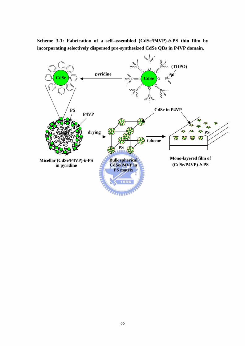
66
Scheme 3-1: Fabrication of a self-assembled (CdSe/P4VP)-b-PS thin film by incorporating selectively dispersed pre-synthesized CdSe QDs in P4VP domain.
Micellar (CdSe/P4VP)-b-PS in pyridine
Mono-layered film of (CdSe/P4VP)-b-PS
drying
CdSe in P4VP PSP4VP
N
N
N
N
NN
NN
CdSe
O
P
O P
O
P
OP
OP
OP
OP
OP
CdSe
PS
PS
pyridine
toluene
Bulk spherical CdSe/P4VP in
PS matrix
(TOPO)
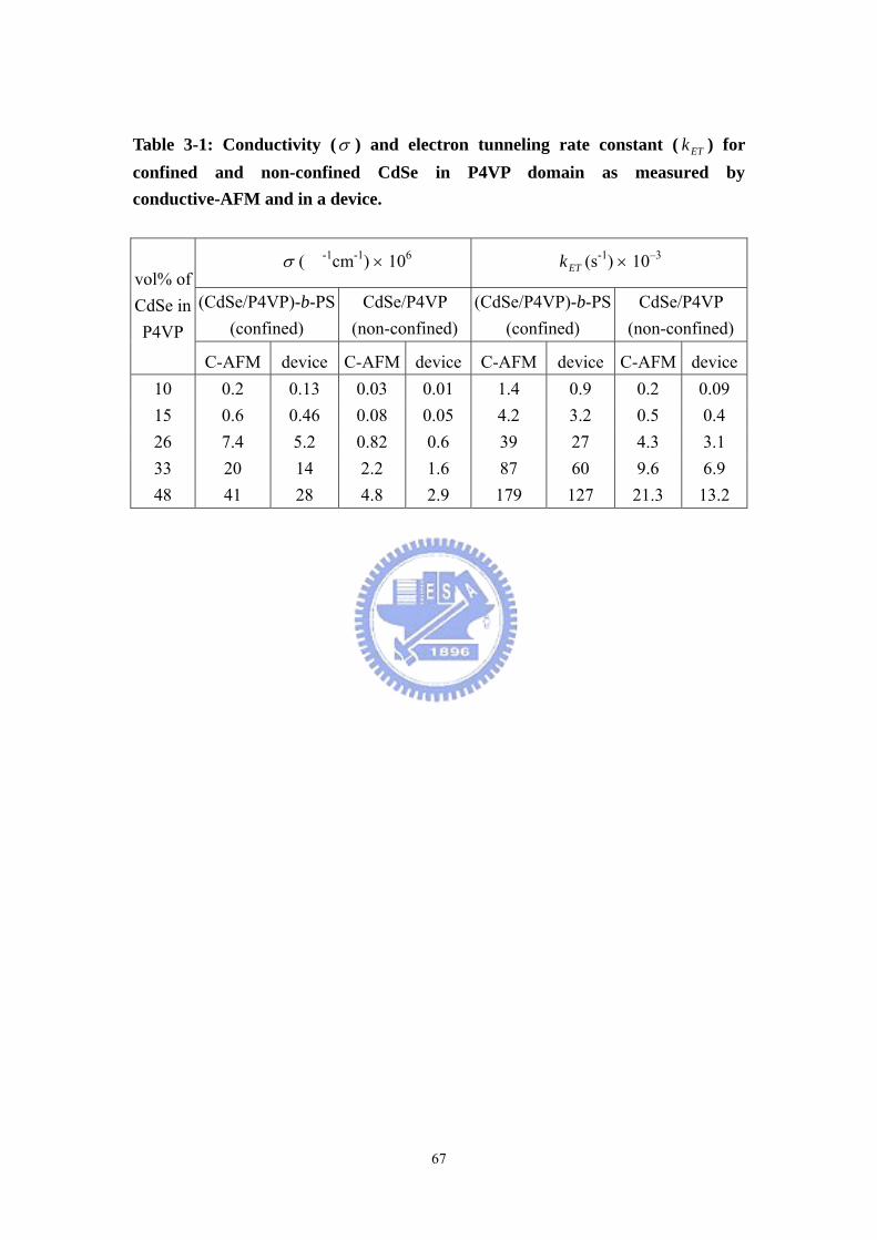
67
Table 3-1: Conductivity (σ ) and electron tunneling rate constant ( ETk ) for confined and non-confined CdSe in P4VP domain as measured by conductive-AFM and in a device.
σ (Ω-1cm-1) × 106 ETk (s-1) × 10–3
(CdSe/P4VP)-b-PS (confined)
CdSe/P4VP (non-confined)
(CdSe/P4VP)-b-PS(confined)
CdSe/P4VP (non-confined)
vol% of CdSe in P4VP
C-AFM device C-AFM device C-AFM device C-AFM device10 0.2 0.13 0.03 0.01 1.4 0.9 0.2 0.09 15 0.6 0.46 0.08 0.05 4.2 3.2 0.5 0.4 26 7.4 5.2 0.82 0.6 39 27 4.3 3.1 33 20 14 2.2 1.6 87 60 9.6 6.9 48 41 28 4.8 2.9 179 127 21.3 13.2
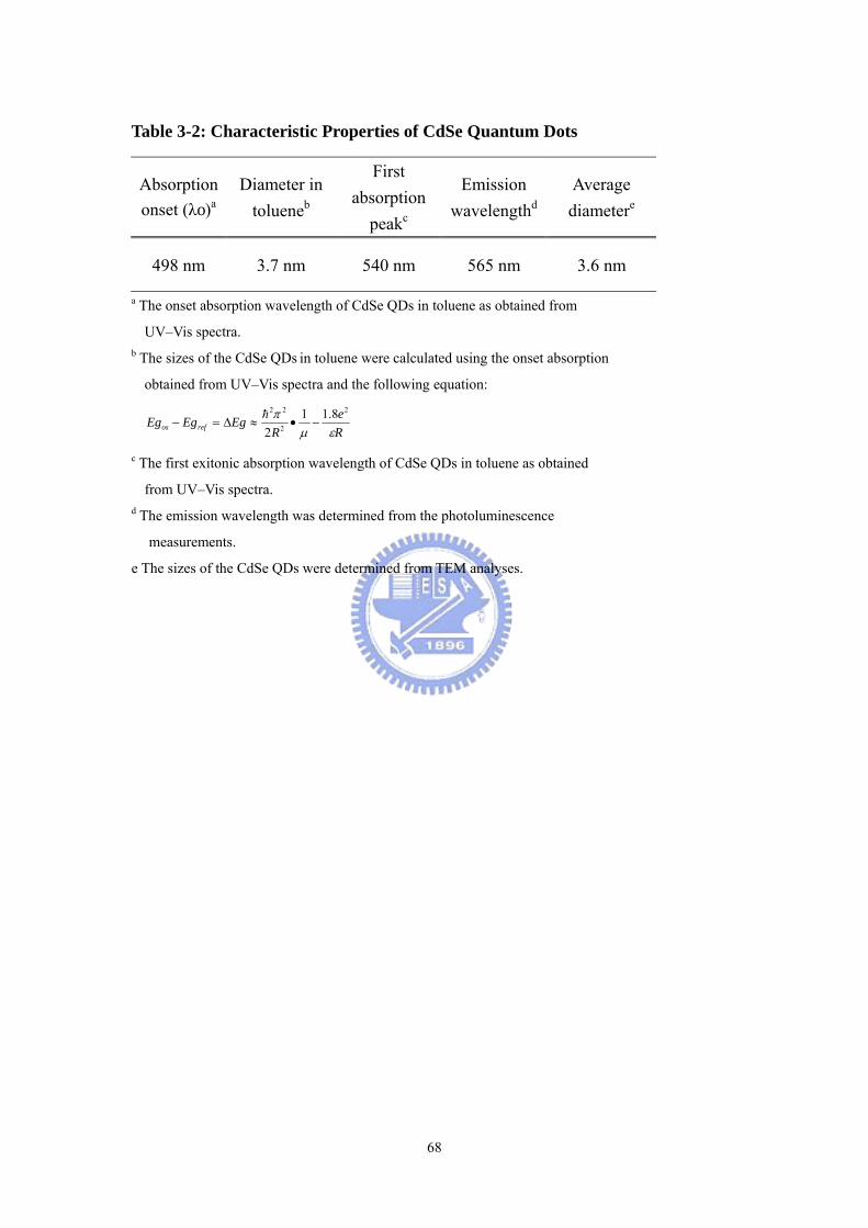
68
Table 3-2: Characteristic Properties of CdSe Quantum Dots
Absorption onset (λo)a
Diameter in tolueneb
First absorption
peakc
Emission wavelengthd
Average diametere
498 nm 3.7 nm 540 nm 565 nm 3.6 nm
a The onset absorption wavelength of CdSe QDs in toluene as obtained from
UV–Vis spectra. b The sizes of the CdSe QDs in toluene were calculated using the onset absorption
obtained from UV–Vis spectra and the following equation:
Re
REgEgEg refos εµ
π 2
2
22 8.112
−•≈∆=−h
c The first exitonic absorption wavelength of CdSe QDs in toluene as obtained
from UV–Vis spectra. d The emission wavelength was determined from the photoluminescence
measurements.
e The sizes of the CdSe QDs were determined from TEM analyses.

69
Table 3-3: Electrical conductivity parameters for the CdSe/P4VP nanodomain
measuring
mode
log cσ
(Ω –1cm–1)
log mσ
(Ω –1cm–1)cϕ F t
C-AFM –6.38 –4.32 0.15 0.5 1.7
device –6.65 –4.58 0.15 0.5 1.7
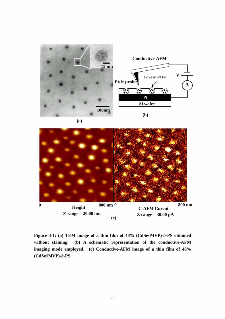
70
Figure 3-1: (a) TEM image of a thin film of 48% (CdSe/P4VP)-b-PS obtained without staining. (b) A schematic representation of the conductive-AFM imaging mode employed. (c) Conductive-AFM image of a thin film of 48% (CdSe/P4VP)-b-PS.
0 800 nm800 nm 0Height C-AFM Curent Z range 20.00 nm Z range 30.00 pA
(c)
V
A
Si wafer
CdSe in P4VP Pt/Ir probe
Pt
(b)
Conductive-AFM
(a)
100nm
15 nm
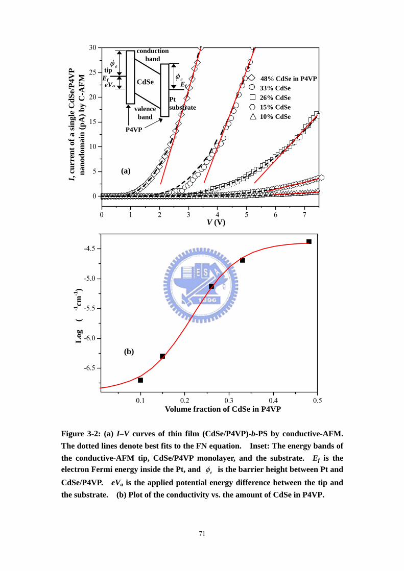
71
Figure 3-2: (a) I–V curves of thin film (CdSe/P4VP)-b-PS by conductive-AFM. The dotted lines denote best fits to the FN equation. Inset: The energy bands of the conductive-AFM tip, CdSe/P4VP monolayer, and the substrate. Ef is the electron Fermi energy inside the Pt, and eφ is the barrier height between Pt and CdSe/P4VP. eVa is the applied potential energy difference between the tip and the substrate. (b) Plot of the conductivity vs. the amount of CdSe in P4VP.
0.1 0.2 0.3 0.4 0.5
-6.5
-6.0
-5.5
-5.0
-4.5
Logσ
(Ω-1
cm-1
)
Volume fraction of CdSe in P4VP
(b)
0 1 2 3 4 5 6 7
0
5
10
15
20
25
30
(a)
V (V)
I, cu
rren
t of a
sing
le C
dSe/
P4V
P na
nodo
mai
n (p
A) b
y C
-AFM
48% CdSe in P4VP
33% CdSe 26% CdSe 15% CdSe 10% CdSe
Pt substrate
tip
CdSe
valence band
conduction band
Ef Ef
- +
P4VP
eφeφ
eVa

72
Figure 3-3: (a) Plot of –ln( σ (CdSe/P4VP)-b-PS) vs. eδ as measured by conductive-AFM and device. (b) Schematic diagram of the barrier height for electron tunneling from the conduction band of CdSe to the LUMO of P4VP and from the Fermi level of Au to the LUMO of an alkanethiol.
5 10 15 20 25
10
12
14
16
= 0.3 Å–1
(a)
– lnσ
(Ω –1
cm–1
)
Average (Å) eδ
(CdSe/P4VP)-b-PS by device
(CdSe/P4VP)-b-PS by C-AFM
dβ
conduction band
vacuum P4VP 100
3. 53 eV
4. 37 eV
= 0.84 eV
e -
e- 0φ
(b)
Fermi level
vacuum Alkylthiol97, 98
2.6~2.9 eV5. 3 eV
= 2.4~2.7 eV
e-
e -
0φ
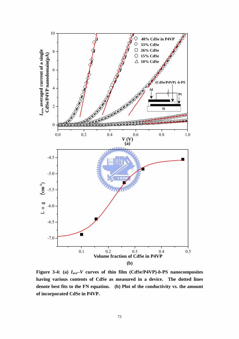
73
Figure 3-4: (a) Iave–V curves of thin film (CdSe/P4VP)-b-PS nanocomposites having various contents of CdSe as measured in a device. The dotted lines denote best fits to the FN equation. (b) Plot of the conductivity vs. the amount of incorporated CdSe in P4VP.
0.1 0.2 0.3 0.4 0.5
-7.0
-6.5
-6.0
-5.5
-5.0
-4.5
Logσ(Ω
-1cm
-1)
Volume fraction of CdSe in P4VP (b)
0.0 0.2 0.4 0.6 0.8 1.0
0
2
4
6
8
10
(a)V (V)
I ave
, ave
rage
d cu
rren
t of a
sing
le
CdS
e/P4
VP
nano
dom
ain(
pA)
Pt Al
(CdSe/P4VP) -b-PS
Si
48% CdSe in P4VP 33% CdSe 26% CdSe 15% CdSe 10% CdSe
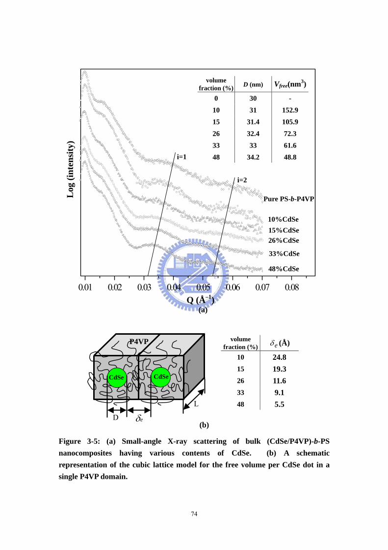
74
Figure 3-5: (a) Small-angle X-ray scattering of bulk (CdSe/P4VP)-b-PS nanocomposites having various contents of CdSe. (b) A schematic representation of the cubic lattice model for the free volume per CdSe dot in a single P4VP domain.
volume fraction (%) D (nm) Vfree(nm3)
0 30 - 10 31 152.9 15 31.4 105.9 26 32.4 72.3 33 33 61.6 48 34.2 48.8
volume fraction (%) eδ (Å)
10 24.8 15 19.3 26 11.6 33 9.1 48 5.5
0.01 0.02 0.03 0.04 0.05 0.06 0.07 0.08
i=1
i=2
Pure PS-b-P4VP
33%CdSe
26%CdSe 15%CdSe
48%CdSe
10%CdSe
Log
(int
ensi
ty)
Q (Å–1) (a)
(b)
CdSe CdSe
D
L
eδ
P4VP
75
Chapter 4: Collective Electron Transport in Au Nanoparticles
Self-Assembled in the Poly(4-vinylpyridine) Nanodomains of a
Poly(styrene-b-4-vinylpyridine) Diblock Copolymer Thin Film
4-1 Introduction
Metal nanoparticles (NPs) that have diameters in the range of 1–10 nm are the
subject of much current research interest because the optical, electronic, and chemical
properties of these materials, such as their single charge tunneling and plasmon
resonances, are size-dependent. [104–106] As a result, such NPs are being investigated
for use in various applications, including memory cells, [107] single-electron transistors,
[108] biological sensors, [109] and catalysts. [110] In these applications, the NPs are often
capped with organic ligands or are surrounded by other dielectric materials. Thus,
an understanding of the collective electron transport of NPs dispersed in organic or
dielectric materials is of both scientific and technological importance. A number of
reports have described two- or three-dimensional electron transport in (a) ordered
arrays of dodecanethiol-capped Ag[111] and Au[112] nanoparticles, Au NPs/SiO2
superlattices,[113] organically capped Co NPs,[114] and CoPt3 NPs[115] and (b)
disordered arrays of granular films of Au NPs linked by alkanethiol molecules[116] and
Au/spacer/CdSe NP assemblies.[117] In contrast, very few reports describe
one-dimensional electron transport within granular films, mainly because of the
difficulties encountered when preparing such samples.
Nanostructured block copolymers that have period thicknesses between 10 and
100 nm, because of microphase separation of incompatible blocks, can be used as
templates to selectively control the spatial arrangement of NPs within one of the
blocks. [118–121] For example, the selective sequestration of pre-synthesized
CdSe,[122a,b] CdS,[134] and TiO2[91a] NPs into one block of a diblock copolymer can be
performed by ensuring that strong interactions exist between that block of the
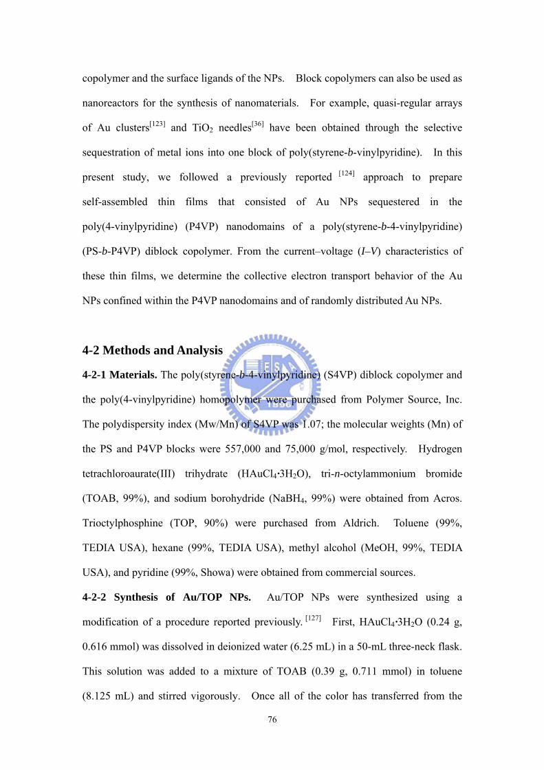
76
copolymer and the surface ligands of the NPs. Block copolymers can also be used as
nanoreactors for the synthesis of nanomaterials. For example, quasi-regular arrays
of Au clusters[123] and TiO2 needles[36] have been obtained through the selective
sequestration of metal ions into one block of poly(styrene-b-vinylpyridine). In this
present study, we followed a previously reported [124] approach to prepare
self-assembled thin films that consisted of Au NPs sequestered in the
poly(4-vinylpyridine) (P4VP) nanodomains of a poly(styrene-b-4-vinylpyridine)
(PS-b-P4VP) diblock copolymer. From the current–voltage (I–V) characteristics of
these thin films, we determine the collective electron transport behavior of the Au
NPs confined within the P4VP nanodomains and of randomly distributed Au NPs.
4-2 Methods and Analysis
4-2-1 Materials. The poly(styrene-b-4-vinylpyridine) (S4VP) diblock copolymer and
the poly(4-vinylpyridine) homopolymer were purchased from Polymer Source, Inc.
The polydispersity index (Mw/Mn) of S4VP was 1.07; the molecular weights (Mn) of
the PS and P4VP blocks were 557,000 and 75,000 g/mol, respectively. Hydrogen
tetrachloroaurate(III) trihydrate (HAuCl4·3H2O), tri-n-octylammonium bromide
(TOAB, 99%), and sodium borohydride (NaBH4, 99%) were obtained from Acros.
Trioctylphosphine (TOP, 90%) were purchased from Aldrich. Toluene (99%,
TEDIA USA), hexane (99%, TEDIA USA), methyl alcohol (MeOH, 99%, TEDIA
USA), and pyridine (99%, Showa) were obtained from commercial sources.
4-2-2 Synthesis of Au/TOP NPs. Au/TOP NPs were synthesized using a
modification of a procedure reported previously. [127] First, HAuCl4·3H2O (0.24 g,
0.616 mmol) was dissolved in deionized water (6.25 mL) in a 50-mL three-neck flask.
This solution was added to a mixture of TOAB (0.39 g, 0.711 mmol) in toluene
(8.125 mL) and stirred vigorously. Once all of the color has transferred from the
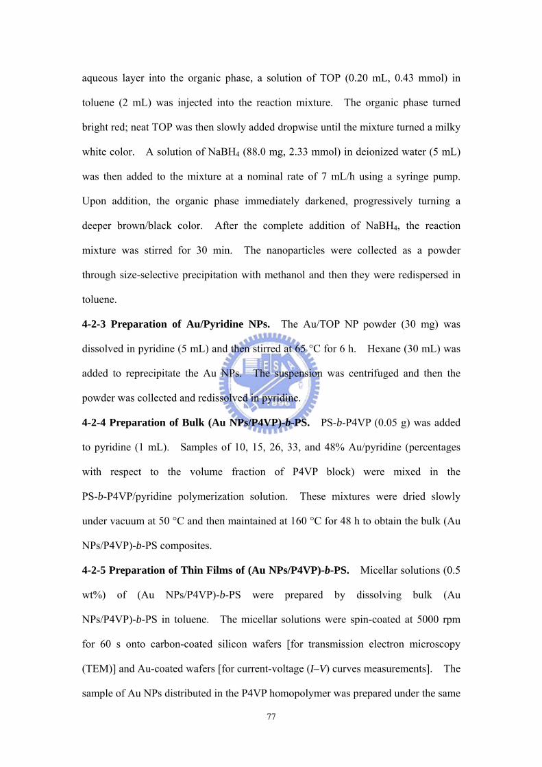
77
aqueous layer into the organic phase, a solution of TOP (0.20 mL, 0.43 mmol) in
toluene (2 mL) was injected into the reaction mixture. The organic phase turned
bright red; neat TOP was then slowly added dropwise until the mixture turned a milky
white color. A solution of NaBH4 (88.0 mg, 2.33 mmol) in deionized water (5 mL)
was then added to the mixture at a nominal rate of 7 mL/h using a syringe pump.
Upon addition, the organic phase immediately darkened, progressively turning a
deeper brown/black color. After the complete addition of NaBH4, the reaction
mixture was stirred for 30 min. The nanoparticles were collected as a powder
through size-selective precipitation with methanol and then they were redispersed in
toluene.
4-2-3 Preparation of Au/Pyridine NPs. The Au/TOP NP powder (30 mg) was
dissolved in pyridine (5 mL) and then stirred at 65 °C for 6 h. Hexane (30 mL) was
added to reprecipitate the Au NPs. The suspension was centrifuged and then the
powder was collected and redissolved in pyridine.
4-2-4 Preparation of Bulk (Au NPs/P4VP)-b-PS. PS-b-P4VP (0.05 g) was added
to pyridine (1 mL). Samples of 10, 15, 26, 33, and 48% Au/pyridine (percentages
with respect to the volume fraction of P4VP block) were mixed in the
PS-b-P4VP/pyridine polymerization solution. These mixtures were dried slowly
under vacuum at 50 °C and then maintained at 160 °C for 48 h to obtain the bulk (Au
NPs/P4VP)-b-PS composites.
4-2-5 Preparation of Thin Films of (Au NPs/P4VP)-b-PS. Micellar solutions (0.5
wt%) of (Au NPs/P4VP)-b-PS were prepared by dissolving bulk (Au
NPs/P4VP)-b-PS in toluene. The micellar solutions were spin-coated at 5000 rpm
for 60 s onto carbon-coated silicon wafers [for transmission electron microscopy
(TEM)] and Au-coated wafers [for current-voltage (I–V) curves measurements]. The
sample of Au NPs distributed in the P4VP homopolymer was prepared under the same
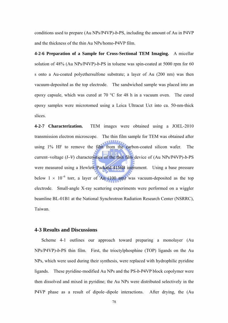
78
conditions used to prepare (Au NPs/P4VP)-b-PS, including the amount of Au in P4VP
and the thickness of the thin Au NPs/homo-P4VP film.
4-2-6 Preparation of a Sample for Cross-Sectional TEM Imaging. A micellar
solution of 48% (Au NPs/P4VP)-b-PS in toluene was spin-coated at 5000 rpm for 60
s onto a Au-coated polyethersulfone substrate; a layer of Au (200 nm) was then
vacuum-deposited as the top electrode. The sandwiched sample was placed into an
epoxy capsule, which was cured at 70 °C for 48 h in a vacuum oven. The cured
epoxy samples were microtomed using a Leica Ultracut Uct into ca. 50-nm-thick
slices.
4-2-7 Characterization. TEM images were obtained using a JOEL-2010
transmission electron microscope. The thin film sample for TEM was obtained after
using 1% HF to remove the film from the carbon-coated silicon wafer. The
current–voltage (I–V) characteristics of the thin film device of (Au NPs/P4VP)-b-PS
were measured using a Hewlett–Packard 4156B instrument. Using a base pressure
below 1 × 10⁻⁶ torr, a layer of Au (100 nm) was vacuum-deposited as the top
electrode. Small-angle X-ray scattering experiments were performed on a wiggler
beamline BL-01B1 at the National Synchrotron Radiation Research Center (NSRRC),
Taiwan.
4-3 Results and Discussions
Scheme 4-1 outlines our approach toward preparing a monolayer (Au
NPs/P4VP)-b-PS thin film. First, the trioctylphosphine (TOP) ligands on the Au
NPs, which were used during their synthesis, were replaced with hydrophilic pyridine
ligands. These pyridine-modified Au NPs and the PS-b-P4VP block copolymer were
then dissolved and mixed in pyridine; the Au NPs were distributed selectively in the
P4VP phase as a result of dipole–dipole interactions. After drying, the (Au
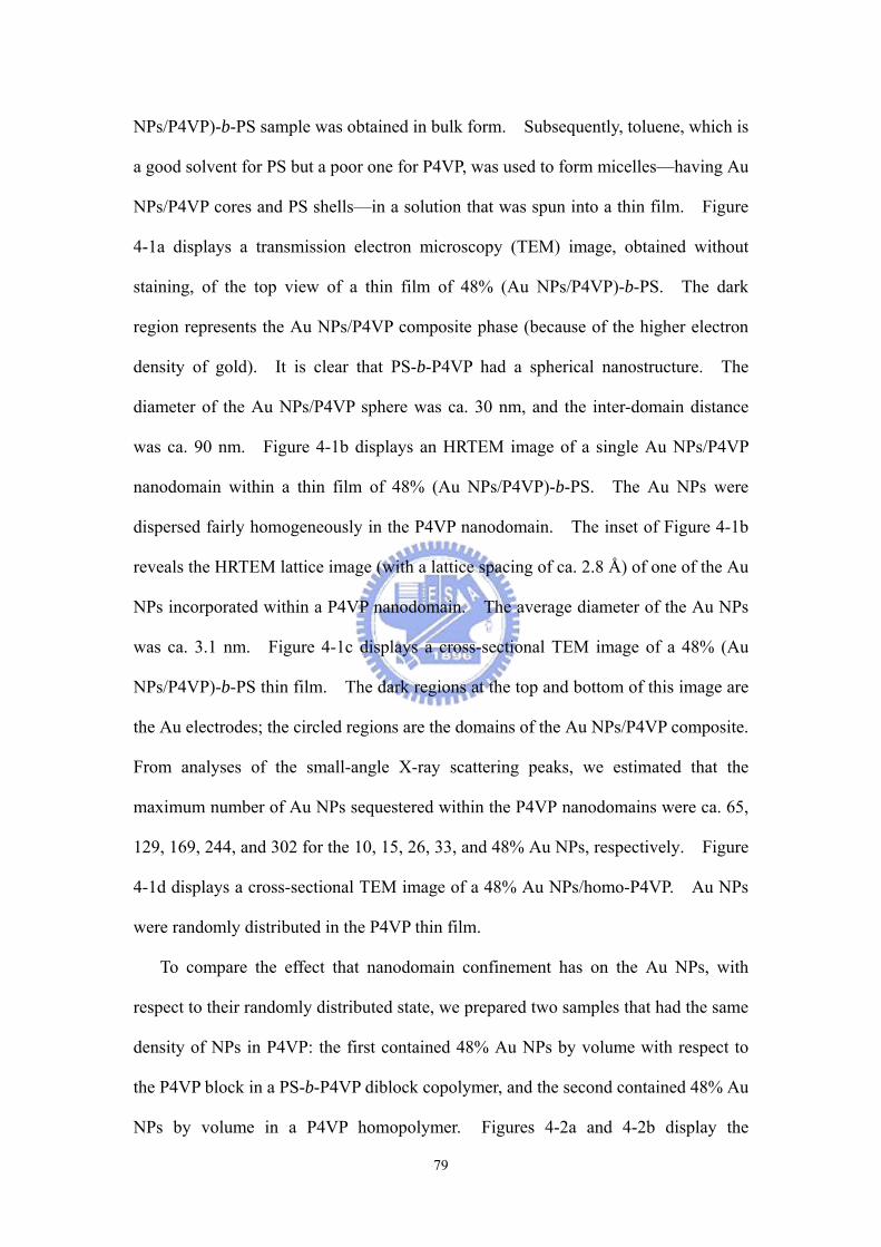
79
NPs/P4VP)-b-PS sample was obtained in bulk form. Subsequently, toluene, which is
a good solvent for PS but a poor one for P4VP, was used to form micelles—having Au
NPs/P4VP cores and PS shells—in a solution that was spun into a thin film. Figure
4-1a displays a transmission electron microscopy (TEM) image, obtained without
staining, of the top view of a thin film of 48% (Au NPs/P4VP)-b-PS. The dark
region represents the Au NPs/P4VP composite phase (because of the higher electron
density of gold). It is clear that PS-b-P4VP had a spherical nanostructure. The
diameter of the Au NPs/P4VP sphere was ca. 30 nm, and the inter-domain distance
was ca. 90 nm. Figure 4-1b displays an HRTEM image of a single Au NPs/P4VP
nanodomain within a thin film of 48% (Au NPs/P4VP)-b-PS. The Au NPs were
dispersed fairly homogeneously in the P4VP nanodomain. The inset of Figure 4-1b
reveals the HRTEM lattice image (with a lattice spacing of ca. 2.8 Å) of one of the Au
NPs incorporated within a P4VP nanodomain. The average diameter of the Au NPs
was ca. 3.1 nm. Figure 4-1c displays a cross-sectional TEM image of a 48% (Au
NPs/P4VP)-b-PS thin film. The dark regions at the top and bottom of this image are
the Au electrodes; the circled regions are the domains of the Au NPs/P4VP composite.
From analyses of the small-angle X-ray scattering peaks, we estimated that the
maximum number of Au NPs sequestered within the P4VP nanodomains were ca. 65,
129, 169, 244, and 302 for the 10, 15, 26, 33, and 48% Au NPs, respectively. Figure
4-1d displays a cross-sectional TEM image of a 48% Au NPs/homo-P4VP. Au NPs
were randomly distributed in the P4VP thin film.
To compare the effect that nanodomain confinement has on the Au NPs, with
respect to their randomly distributed state, we prepared two samples that had the same
density of NPs in P4VP: the first contained 48% Au NPs by volume with respect to
the P4VP block in a PS-b-P4VP diblock copolymer, and the second contained 48% Au
NPs by volume in a P4VP homopolymer. Figures 4-2a and 4-2b display the
80
averaged I–V characteristics of the monolayer (Au NPs/P4VP)-b-PS and Au
NPs/P4VP thin films, both measured at temperatures within the range from 250 to 78
K. In both cases, the I–V curves were ohmic at 250 K, but become increasingly
nonlinear upon decreasing the temperature. At 100 K and below, conduction
occurred through the composite only at potentials above a minimum threshold voltage,
VT, which indicates that a collective Coulomb blockade resulted from electrical
isolation of the NPs. A model for low-voltage electron transport through an array of
Coulomb islands predicts thermally activated behavior for the zero-bias conductance:
[112–115,125]
−
∝Tk
EGB
aexp0 (4-1)
where 0G is the zero-bias conductance, aE is the activation energy to charge an
electrically neutral nanocrystal, Bk is the Boltzmann constant, and T is the
temperature. The insets to Figures 4-2a and 4-2b present plots of 0ln G vs. T/1 .
From the slopes of the theoretical fits obtained using Eq. (4-1), we calculated the
experimental values for the activation energies ( aE ) of the nanodomain-confined and
randomly distributed samples to be 27 and 28 meV, respectively. The value of aE
can be expressed as Ce 22 , where e is the charge of the electron and C is the
total capacitance of a nanoparticle, resulting from the inter-nanoparticle capacitance,
iC , and the nanoparticle self-capacitance, sC . Neglecting the small contribution to
C from sC , we obtained ( )[ ])2//(2/ln2 0 ddrrnCnC i +⋅≈⋅≈ επε , where ε is
the dielectric constant of the surrounding P4VP matrix (ca. 3), r is the nanoparticle
radius (1.5 nm), d is the interparticle distance (0.55 nm), and n is the average
number of nearest neighbors (assuming each nanoparticle has an average of between
six to twelve nearest neighbors).[114, 126] We estimated that the total capacitance (C)
would be between 2.3 and 4.5 aF; therefore, we calculated the activation energy to be
81
35–17.5 meV ( CeEa 2/2≈ ). Thus, the experimental values of the activation
energies within both the nanodomain-confined and randomly distributed samples are
in reasonable agreement with the calculated values. Figure 4-2c displays
representative current–voltage scaling data obtained for these two samples at 78 K.
The accessible current-conducting pathways are described [112–115,124] by Eq. (4-2):
ζ
−∝ 1
TVVI (4-2)
(for V > VT ), where I is the current, V is the voltage, ζ is a scaling exponent,
and TV is the threshold voltage. The scaling exponent ζ can be regarded as the
dimensionality for collective electron transport for arrays of dots as modeled in a
previous study. [124] We obtained power-law scalings ( ζ ) of 1.31 for the
nanodomain-confined sample and 2.84 for the randomly distributed sample. These
results indicate that quasi-one-dimensional collective electron transport occurs for the
nanodomain-confined Au NPs and that quasi-three-dimensional collective electron
transport occurs for the randomly distributed Au NPs. Figure 4-2d presents a plot of
TV vs. d for nanodomain-confined and randomly distributed samples having
various Au NP contents. The values of TV of the Au NPs in the P4VP domains of
PS-b-P4VP were ca. 14% smaller than those of the Au NPs in the homo-P4VP. In
both cases, the values of TV of these composites increased linearly upon increasing
the interparticle distance, because the pathway of collective electron transport
increases with respect to the interparticle distance (see inset of Figure 4-2d). [124]
Figure 4-3a displays one-dimensional small-angle X-ray scattering patterns
(SAXS) of (Au NPs/P4VP)-b-PS obtained using synchrotron radiation. The
scattering maxima, which are denoted by the letter “i” (i = 1), are form factor peaks
associated with scattering from the isolated spherical domains. The form factor
peaks shifted slightly to lower values of Q as the amount of incorporated Au increased,

82
which indicates that the volume or size of the Au NPs/P4VP composite domains
increased. The average diameter of the P4VP domains of pure PS-b-P4VP, deduced
from the positions of the form factor maxima, was 26.6 nm. The average diameters,
measured by their volume, for the 10, 15, 26, 33, and 48% Au NPs in the P4VP block
were 27.3, 27.8, 28.6, 29.3, and 30.2 nm, respectively, assuming that the density of
P4VP and Au remained the same before and after mixing. The inset of Figure 4-3a
lists the free volume per Au particle in a single P4VP domain ( freeV ), which is defined
by the average volume of an occupied Au particle and can be estimated using Eqs.
(4-3) and (4-4):
nV
VVAu
VPPVPPAu =− 44/ (4-3)
freeVPPAu V
nV
=4/ (4-4)
where VPPAuV 4/ is the volume of a single Au NPs/P4VP composite domain,
VPPV 4 is the volume of a single P4VP domain, AuV is the volume of a Au NP, and n
is the maximum number of Au NPs in a single P4VP domain. The edge-to-edge
interparticle distance ( d ) can be determined by assuming a cubic lattice model for the
Au NPs. The values of d were calculated using Eq. (4-5) based on the cubic
lattice model presented in Figure 4-3b. [128]
( ) rVrLd free 22 3/1 −=−= (4-5)
where r is the radius of the Au NPs. The value of d decreased when the
amount of Au increased, as displayed in the inset of Figure 4-3b.
Figures 4-5a and 4-6a display the I–V characteristics, measured at 78 K, of
monolayer (Au NPs/P4VP)-b-PS and Au NPs/homo-P4VP thin films, respectively,
having various contents of Au. For the (Au NPs/P4VP)-b-PS samples, the current
was assumed to flow through the Au/P4VP nanodomain, owing to the much higher
83
resistance of the PS phase. The conductivity of the Au NPs/P4VP composite
increased monotonically when the amount of Au increased, both in the
nanodomain-confined and randomly distributed samples. Figures 4-5b and 4-6b
display representative I–V scaling data, recorded at 78 K, for (Au NPs/P4VP)-b-PS
and Au NPs/homo-P4VP thin films having various contents of Au. Table 4-1
provides details regarding the fitting of the curves and the calculation of the threshold
voltages and scaling exponents. The data in Figure 4-5b provide power-law scalings,
ζ , for the 15, 26, 33, and 48% Au NPs of 1.42, 1.39, 1.32, and 1.31, respectively.
These values indicate that the effect of nanodomain confinement for
quasi-one-dimensional collective electron transport for Au NPs in a nanodomain
decreases when the number of Au NPs decreases. The data in Figure 4-6b provide
power-law scalings, ζ , for the 15, 26, 33, and 48% Au NPs of 2.89, 2.89, 2.87, and
2.84, respectively. These values indicate that the dimensionality for collective
electron transport in the randomly distributed sample is independent of the number of
Au NPs; i.e., quasi-three-dimensional collective electron transport occurs for the
randomly distributed Au NPs.
4-4 Conclusions
We have demonstrated that the collective electron transport behavior between Au
NPs confined within a single P4VP nanodomain is quasi one-dimensional, as opposed
to the three-dimensional behavior displayed by Au NPs in homo-P4VP. The
threshold voltage of these composite increased linearly upon increasing the
inter-nanoparticle distance for both the nanodomain-confined and randomly
distributed samples.
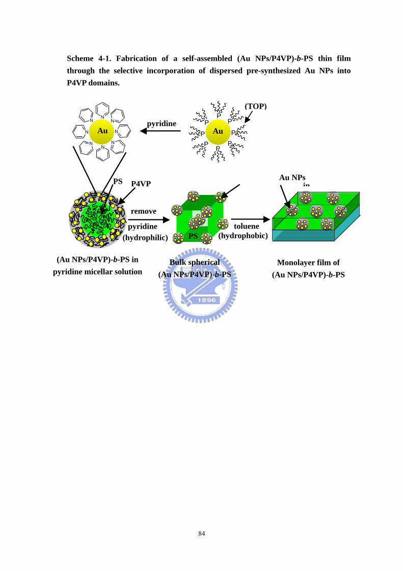
84
Scheme 4-1. Fabrication of a self-assembled (Au NPs/P4VP)-b-PS thin filmthrough the selective incorporation of dispersed pre-synthesized Au NPs intoP4VP domains.
(Au NPs/P4VP)-b-PS in pyridine micellar solution
Bulk spherical (Au NPs/P4VP)-b-PS
Monolayer film of (Au NPs/P4VP)-b-PS
(hydrophilic)pyridine
remove
toluene
Au NPs in
(hydrophobic)
pyridine
(TOP)
Au
PP
PP
P
P
P
P
N
N
N
N
NN
NN
Au
PS P4VP
PS
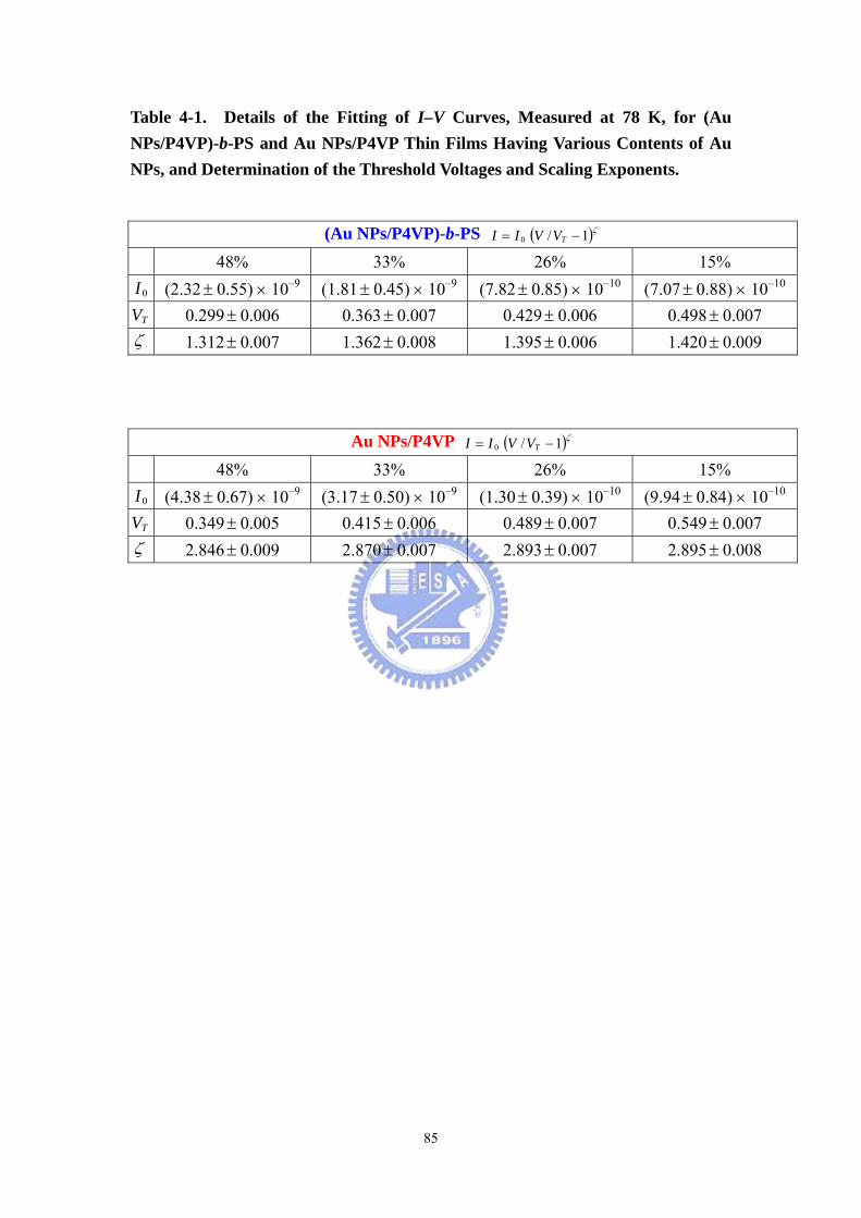
85
Table 4-1. Details of the Fitting of I–V Curves, Measured at 78 K, for (Au NPs/P4VP)-b-PS and Au NPs/P4VP Thin Films Having Various Contents of Au NPs, and Determination of the Threshold Voltages and Scaling Exponents.
(Au NPs/P4VP)-b-PS ( )ζ1/0 −= TVVII 48% 33% 26% 15%
0I (2.32 ± 0.55) × 10–9 (1.81 ± 0.45) × 10–9 (7.82 ± 0.85) × 10–10 (7.07 ± 0.88) × 10–10
TV 0.299 ± 0.006 0.363 ± 0.007 0.429 ± 0.006 0.498 ± 0.007 ζ 1.312 ± 0.007 1.362 ± 0.008 1.395 ± 0.006 1.420 ± 0.009
Au NPs/P4VP ( )ζ1/0 −= TVVII 48% 33% 26% 15%
0I (4.38 ± 0.67) × 10–9 (3.17 ± 0.50) × 10–9 (1.30 ± 0.39) × 10–10 (9.94 ± 0.84) × 10–10
TV 0.349 ± 0.005 0.415 ± 0.006 0.489 ± 0.007 0.549 ± 0.007 ζ 2.846 ± 0.009 2.870 ± 0.007 2.893 ± 0.007 2.895 ± 0.008
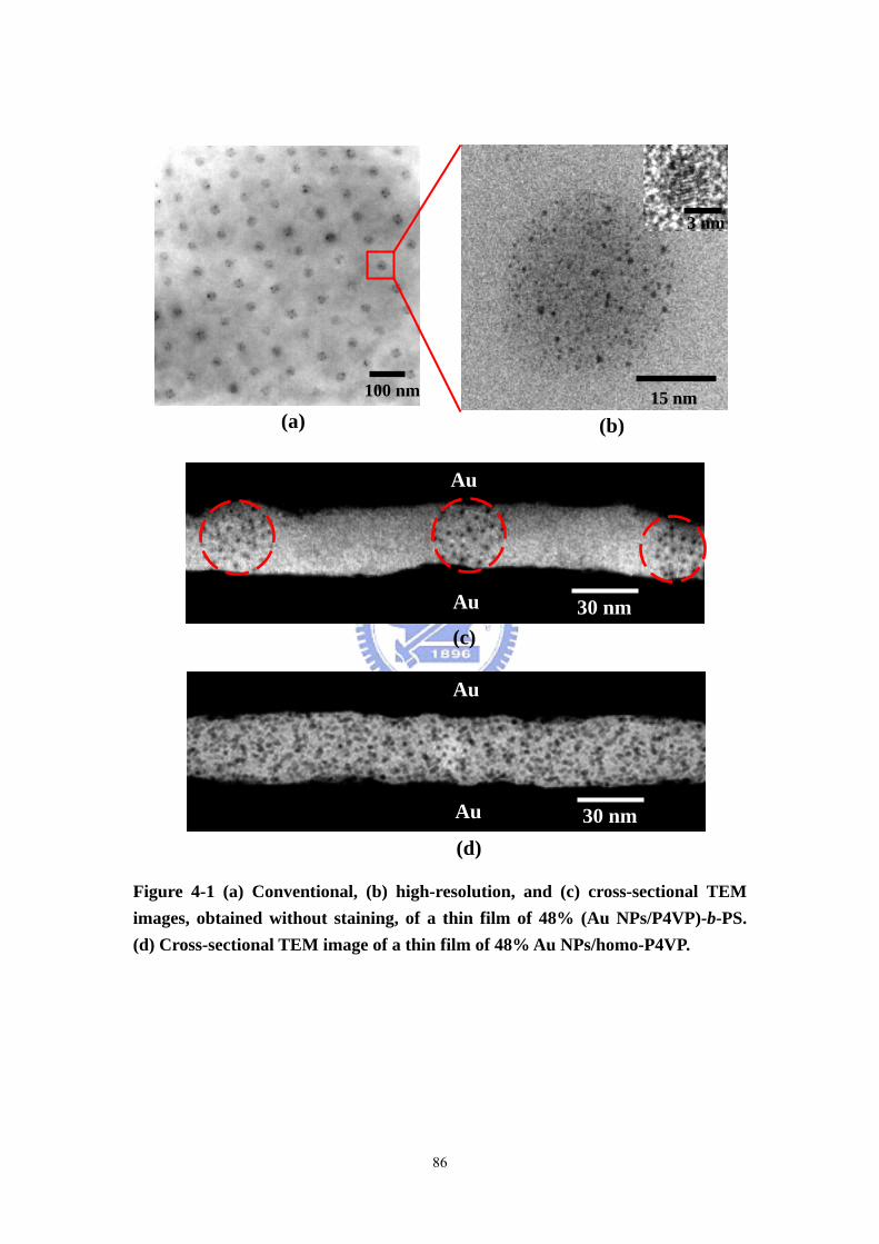
86
Figure 4-1 (a) Conventional, (b) high-resolution, and (c) cross-sectional TEM images, obtained without staining, of a thin film of 48% (Au NPs/P4VP)-b-PS. (d) Cross-sectional TEM image of a thin film of 48% Au NPs/homo-P4VP.
(a) (b)
3 nm
15 nm 100 nm
Au
Au
30 nm (c)
Au
Au
30 nm (d)
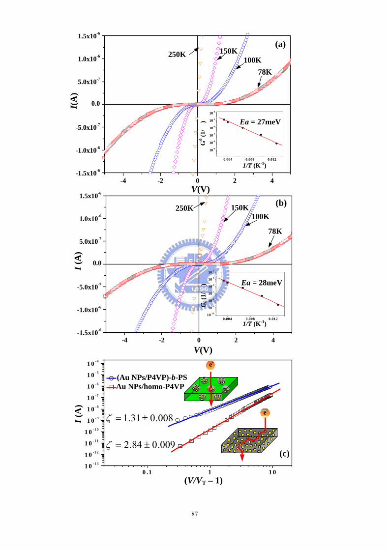
87
-4 -2 0 2 4-1.5x10⁻⁶
-1.0x10⁻⁶
-5.0x10⁻⁷
0.0
5.0x10⁻⁷
1.0x10⁻⁶
1.5x10⁻⁶
250K 150K100K
78K
V(V)
I(A
)
(a)
0.004 0.008 0.012
10-9
10-8
10-7
10-6
10-5
10-4
G0 (1
/Ω)
1/T (K-1)
Ea = 27meV
-4 -2 0 2 4-1.5x10⁻⁶
-1.0x10⁻⁶
-5.0x10⁻⁷
0.0
5.0x10⁻⁷
1.0x10⁻⁶
1.5x10⁻⁶
250K 150K100K
78K
I (A
)
V(V)
(b)
0.004 0.008 0.01210-10
10-9
10-8
10-7
10-6
10-5
10-4
G0 (1
/Ω)
1/T (K-1)
Ea = 28meV
0 .1 1 1 01 0 -1 3
1 0 -1 2
1 0 -1 1
1 0 -1 0
1 0 -9
1 0 -8
1 0 -7
1 0 -6
1 0 -5
1 0 -4
e-
I (A
)
(Au NPs/P4VP)-b-PS Au NPs/homo-P4VP
e-
008.031.1 ±=ζ
009.084.2 ±=ζ
(V/VT – 1)
(c)

88
(Au NPs/P4VP)-b-PS Au NPs/homo-P4VP
0.4 0.6 0.8 1.0 1.2 1.4 1.60.20
0.25
0.30
0.35
0.40
0.45
0.50
0.55
0.60
0.65
Interparticle distance (nm)
VT (V
)
e-e-
(d)
Figure 4-2 I–V curves of (a) 48% (Au NPs/P4VP)-b-PS and (b) Au NPs/homo-P4VP thin films measured at temperatures between 250 and 78 K. (c) Scaling behavior of the I–V curves of 48% (Au NPs/P4VP)-b-PS and Au NPs/homo-P4VP at 78 K. (d) Plots of VT vs. d for the 48% (Au NPs/P4VP)-b-PS and Au NPs/homo-P4VP samples having various contents of Au NPs.
volume fraction (%) d (nm)
10 2.41 15 1.42 26 1.16 33 0.79 48 0.55
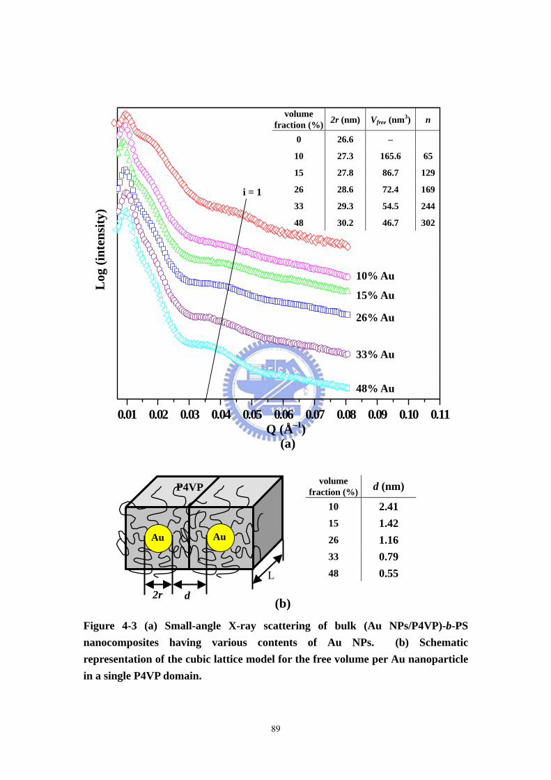
89
0.01 0.02 0.03 0.04 0.05 0.06 0.07 0.08 0.09 0.10 0.11
i = 1
33% Au
26% Au
15% Au
48% Au
10% Au
Log
(int
ensi
ty)
Q (Å–1) (a)
Figure 4-3 (a) Small-angle X-ray scattering of bulk (Au NPs/P4VP)-b-PS nanocomposites having various contents of Au NPs. (b) Schematic representation of the cubic lattice model for the free volume per Au nanoparticle in a single P4VP domain.
volume fraction (%) 2r (nm) Vfree (nm3) n
0 26.6 –
10 27.3 165.6 65
15 27.8 86.7 129
26 28.6 72.4 169
33 29.3 54.5 244
48 30.2 46.7 302
volume fraction (%) d (nm)
10 2.41 15 1.42 26 1.16 33 0.79 48 0.55
(b)2r
Au Au
L
P4VP
d
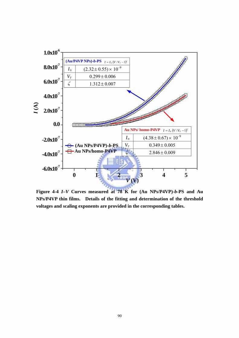
90
Figure 4-4 I–V Curves measured at 78 K for (Au NPs/P4VP)-b-PS and Au NPs/P4VP thin films. Details of the fitting and determination of the threshold voltages and scaling exponents are provided in the corresponding tables.
(Au/P4VP NPs)-b-PS ( )ζ1/0 −= TVVII
0I (2.32 ± 0.55) × 10–9 TV 0.299 ± 0.006
ζ 1.312 ± 0.007
Au NPs/ homo-P4VP ( )ζ1/0 −= TVVII
0I (4.38 ± 0.67) × 10–9 TV 0.349 ± 0.005
ζ 2.846 ± 0.009
0 1 2 3 4 5-6.0x10⁻⁷
-4.0x10⁻⁷
-2.0x10⁻⁷
0.0
2.0x10⁻⁷
4.0x10⁻⁷
6.0x10⁻⁷
8.0x10⁻⁷
1.0x10⁻⁶
V (V)
I (A
)
(Au NPs/P4VP)-b-PS Au NPs/homo-P4VP
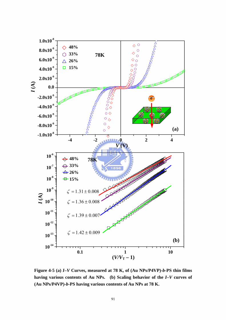
91
Figure 4-5 (a) I–V Curves, measured at 78 K, of (Au NPs/P4VP)-b-PS thin films having various contents of Au NPs. (b) Scaling behavior of the I–V curves of (Au NPs/P4VP)-b-PS having various contents of Au NPs at 78 K.
-4 -2 0 2 4-1.0x10⁻⁸
-8.0x10⁻⁹
-6.0x10⁻⁹
-4.0x10⁻⁹
-2.0x10⁻⁹
0.0
2.0x10⁻⁹
4.0x10⁻⁹
6.0x10⁻⁹
8.0x10⁻⁹
1.0x10⁻⁸
48% 33% 26% 15%
V (V)
I (A
)
78K
e-
(a)
0.1 1 1010-14
10-13
10-12
10-11
10-10
10-9
10-8
10-7
10-6
(V/VT – 1)
I (A
) 008.031.1 ±=ζ
009.042.1 ±=ζ
48% 33% 26% 15%
008.036.1 ±=ζ
007.039.1 ±=ζ
78K
(b)
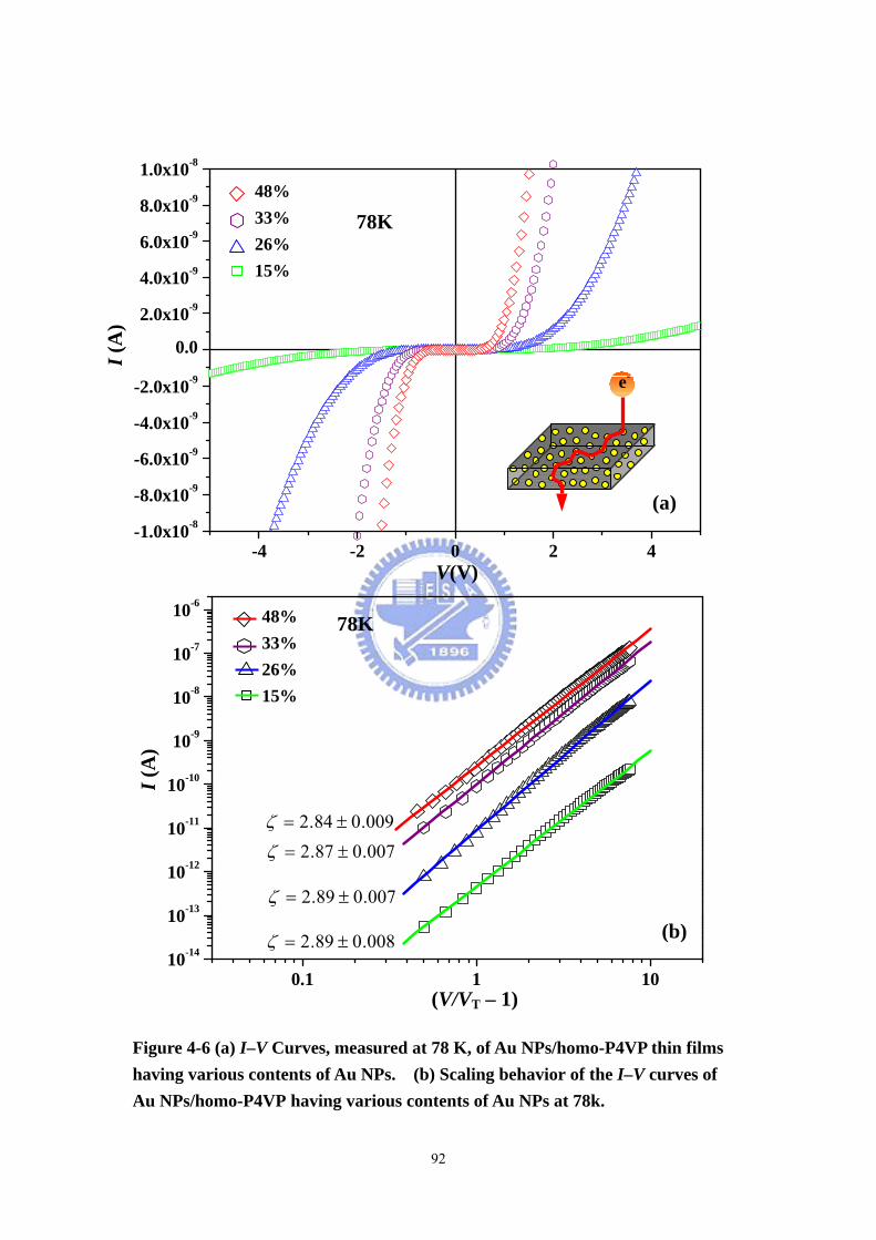
92
-4 -2 0 2 4-1.0x10⁻⁸
-8.0x10⁻⁹
-6.0x10⁻⁹
-4.0x10⁻⁹
-2.0x10⁻⁹
0.0
2.0x10⁻⁹
4.0x10⁻⁹
6.0x10⁻⁹
8.0x10⁻⁹
1.0x10⁻⁸
48% 33% 26% 15%
V(V)
I (A
)
78K
e-
(a)
Figure 4-6 (a) I–V Curves, measured at 78 K, of Au NPs/homo-P4VP thin films having various contents of Au NPs. (b) Scaling behavior of the I–V curves of Au NPs/homo-P4VP having various contents of Au NPs at 78k.
0.1 1 1010-14
10-13
10-12
10-11
10-10
10-9
10-8
10-7
10-6
(V/VT – 1)
I (A
)
48% 33% 26% 15%
78K
009.084.2 ±=ζ
008.089.2 ±=ζ
007.087.2 ±=ζ
007.089.2 ±=ζ
(b)
93
Chapter 5: The Orientation of CdSe Nanorods Affects the Electron
Mobility of CdSe/P4VP Nanodomains Self-Assembled within a
Poly(styrene-b-4-vinylpyridine) Diblock Copolymer Thin Film
5-1 Introduction
Block copolymers are versatile platform materials because they can
self-assemble—if they have appropriate compositions and are subjected to suitable
conditions—into various nanostructures having period thicknesses between 10 and
100 nm through microphase separation of incompatible blocks. [129,130]
Nanostructured block copolymers can be used as templates for selectively controlling
the spatial position of semiconductor nanoparticles within one of the blocks.[131–133]
For example, the selective sequestrations of pre-synthesized CdS,[20, 22, 134] CdSe,[131c]
and TiO2[91a] nanoparticles into one block of a diblock copolymers can be performed
by ensuring the presence of strong interactions between that block and the surface
ligands of the nanoparticles. Block copolymers can also be used as nanoreactors for
the synthesis of nanomaterials. For example, quasi-regular arrays of Au clusters [133a]
and TiO2 needles [36] have been obtained through the selective sequestration of metal
ions into one block of poly(styrene-b-vinylpyridine).
The unique optical and electrical properties of one-dimensional (1D)
semiconductor nanostructures, such as nanorods (NRs) and nanowires (NWs), can be
exploited for use in a number of applications, including solar cells, photonic crystals,
lasers, transistors, and sensors. [135, 136, 139a,b] To take full advantage of the material
properties of these 1D nanostructures, they must be pre-aligned or ordered in some
other way. Several physical and chemical strategies have been used for the
alignment or ordering of arrays 1D nanostructures. Examples for in-plane
two-dimensional (2D) arrays include the unidirectional alignment of CdSe NRs, [137]
the assembly of BaCrO4 NR monolayers through the use of the Langmuir–Blodgett

94
technique, [138] and the alignment of a liquid-crystalline phase of CdSe NRs through
surface deposition. [139c] For out-of-plane 2D arrays, some examples are the use of
e-beam lithography to obtain arrays of CdSe pillars and TiO2 nanoneedles through
electrochemical deposition and solution crystal growth,[140, 91b] and the preparation of
a periodic array of uniform ZnO NWs through vapor phase transport and catalytic
growth.[141] Although there are many bottom-up growth techniques for preparing 1D
nanostructures in the out-of-plane 2D arrays and many techniques for pre-synthesized
NRs in the in-plane 2D arrays, finding techniques for arranging pre-synthesized NRs
in out-of-plane 2D arrays remains a great challenge.
The powerful aligning force of an electric field can be used to manipulate the
orientation of anisotropic materials by taking advantage of their different anisotropic
dielectric constants. Examples of this approach include the alignment of ZnO NRs
and Au NWs, [142] the alignment of carbon nanotubes suspended in a columnar
liquid-crystalline polymer melt, [143] and the electrically induced sphere-to-cylinder
transition and pattering in diblock copolymers films. [144] In this present study, we
applied an electric field to induce the orientation of CdSe NRs that had been
self-assembled in the poly(4-vinylpyridine) (P4VP) nanodomains of a
poly(styrene-b-4-vinylpyridine) (PS-b-P4VP) diblock copolymer thin film. We
varied the number of CdSe nanorods incorporated in the P4VP nanodomains by
controlling the strength of the polar interactions and the loading concentration. The
electron mobilities and the electron barrier heights of the CdSe/P4VP nanodomains
incorporating out-of-plane and in-plane CdSe nanorods were monitored.
5-2 Methods and Analysis
5-2-1 Materials. The poly(styrene-b-4-vinylpyridine) (S4VP) diblock copolymer was
purchased from Polymer Source, Inc. The polydispersity index (Mw/Mn) was 1.07;
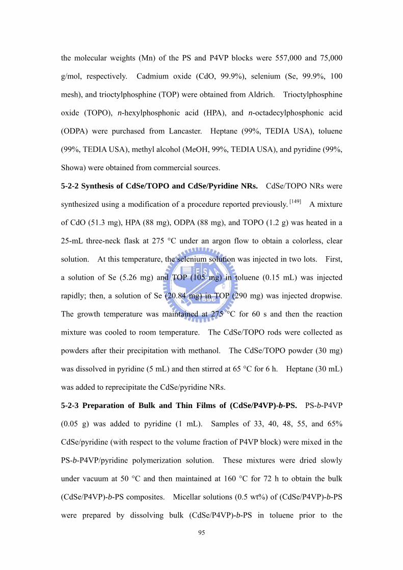
95
the molecular weights (Mn) of the PS and P4VP blocks were 557,000 and 75,000
g/mol, respectively. Cadmium oxide (CdO, 99.9%), selenium (Se, 99.9%, 100
mesh), and trioctylphosphine (TOP) were obtained from Aldrich. Trioctylphosphine
oxide (TOPO), n-hexylphosphonic acid (HPA), and n-octadecylphosphonic acid
(ODPA) were purchased from Lancaster. Heptane (99%, TEDIA USA), toluene
(99%, TEDIA USA), methyl alcohol (MeOH, 99%, TEDIA USA), and pyridine (99%,
Showa) were obtained from commercial sources.
5-2-2 Synthesis of CdSe/TOPO and CdSe/Pyridine NRs. CdSe/TOPO NRs were
synthesized using a modification of a procedure reported previously. [149] A mixture
of CdO (51.3 mg), HPA (88 mg), ODPA (88 mg), and TOPO (1.2 g) was heated in a
25-mL three-neck flask at 275 °C under an argon flow to obtain a colorless, clear
solution. At this temperature, the selenium solution was injected in two lots. First,
a solution of Se (5.26 mg) and TOP (105 mg) in toluene (0.15 mL) was injected
rapidly; then, a solution of Se (20.84 mg) in TOP (290 mg) was injected dropwise.
The growth temperature was maintained at 275 °C for 60 s and then the reaction
mixture was cooled to room temperature. The CdSe/TOPO rods were collected as
powders after their precipitation with methanol. The CdSe/TOPO powder (30 mg)
was dissolved in pyridine (5 mL) and then stirred at 65 °C for 6 h. Heptane (30 mL)
was added to reprecipitate the CdSe/pyridine NRs.
5-2-3 Preparation of Bulk and Thin Films of (CdSe/P4VP)-b-PS. PS-b-P4VP
(0.05 g) was added to pyridine (1 mL). Samples of 33, 40, 48, 55, and 65%
CdSe/pyridine (with respect to the volume fraction of P4VP block) were mixed in the
PS-b-P4VP/pyridine polymerization solution. These mixtures were dried slowly
under vacuum at 50 °C and then maintained at 160 °C for 72 h to obtain the bulk
(CdSe/P4VP)-b-PS composites. Micellar solutions (0.5 wt%) of (CdSe/P4VP)-b-PS
were prepared by dissolving bulk (CdSe/P4VP)-b-PS in toluene prior to the
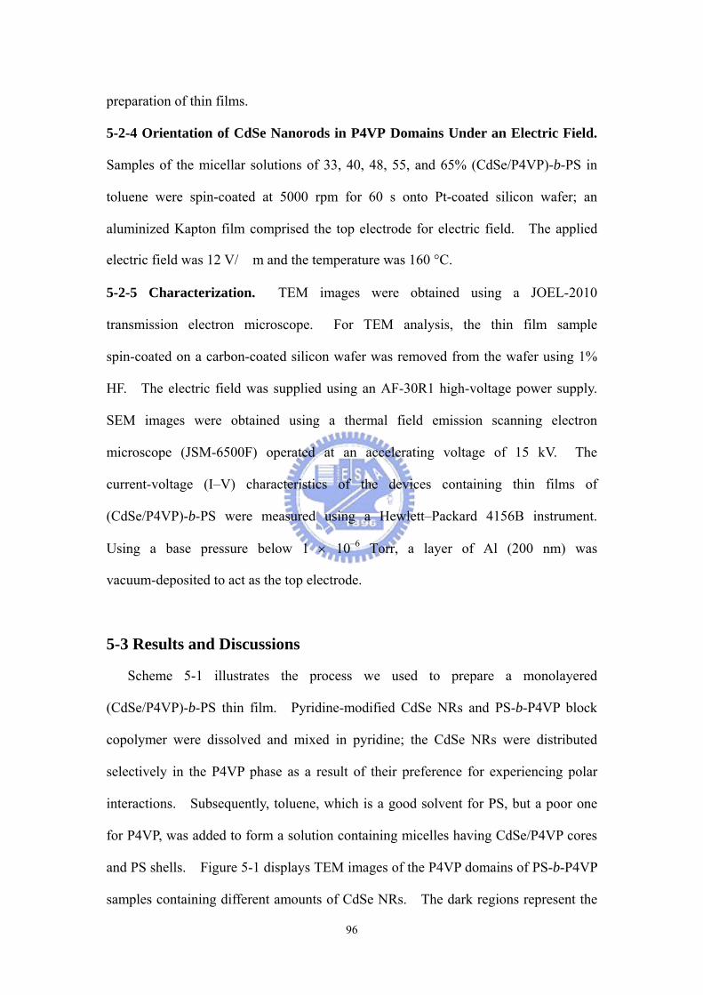
96
preparation of thin films.
5-2-4 Orientation of CdSe Nanorods in P4VP Domains Under an Electric Field.
Samples of the micellar solutions of 33, 40, 48, 55, and 65% (CdSe/P4VP)-b-PS in
toluene were spin-coated at 5000 rpm for 60 s onto Pt-coated silicon wafer; an
aluminized Kapton film comprised the top electrode for electric field. The applied
electric field was 12 V/μm and the temperature was 160 °C.
5-2-5 Characterization. TEM images were obtained using a JOEL-2010
transmission electron microscope. For TEM analysis, the thin film sample
spin-coated on a carbon-coated silicon wafer was removed from the wafer using 1%
HF. The electric field was supplied using an AF-30R1 high-voltage power supply.
SEM images were obtained using a thermal field emission scanning electron
microscope (JSM-6500F) operated at an accelerating voltage of 15 kV. The
current-voltage (I–V) characteristics of the devices containing thin films of
(CdSe/P4VP)-b-PS were measured using a Hewlett–Packard 4156B instrument.
Using a base pressure below 1 × 10⁻⁶ Torr, a layer of Al (200 nm) was
vacuum-deposited to act as the top electrode.
5-3 Results and Discussions
Scheme 5-1 illustrates the process we used to prepare a monolayered
(CdSe/P4VP)-b-PS thin film. Pyridine-modified CdSe NRs and PS-b-P4VP block
copolymer were dissolved and mixed in pyridine; the CdSe NRs were distributed
selectively in the P4VP phase as a result of their preference for experiencing polar
interactions. Subsequently, toluene, which is a good solvent for PS, but a poor one
for P4VP, was added to form a solution containing micelles having CdSe/P4VP cores
and PS shells. Figure 5-1 displays TEM images of the P4VP domains of PS-b-P4VP
samples containing different amounts of CdSe NRs. The dark regions represent the
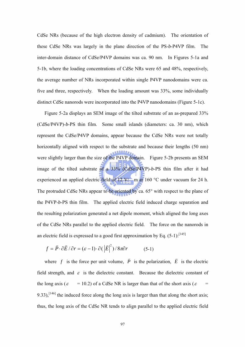
97
CdSe NRs (because of the high electron density of cadmium). The orientation of
these CdSe NRs was largely in the plane direction of the PS-b-P4VP film. The
inter-domain distance of CdSe/P4VP domains was ca. 90 nm. In Figures 5-1a and
5-1b, where the loading concentrations of CdSe NRs were 65 and 48%, respectively,
the average number of NRs incorporated within single P4VP nanodomains were ca.
five and three, respectively. When the loading amount was 33%, some individually
distinct CdSe nanorods were incorporated into the P4VP nanodomains (Figure 5-1c).
Figure 5-2a displays an SEM image of the tilted substrate of an as-prepared 33%
(CdSe/P4VP)-b-PS thin film. Some small islands (diameters: ca. 30 nm), which
represent the CdSe/P4VP domains, appear because the CdSe NRs were not totally
horizontally aligned with respect to the substrate and because their lengths (50 nm)
were slightly larger than the size of the P4VP domain. Figure 5-2b presents an SEM
image of the tilted substrate of a 33% (CdSe/P4VP)-b-PS thin film after it had
experienced an applied electric field of 12 V/μm at 160 °C under vacuum for 24 h.
The protruded CdSe NRs appear to be oriented by ca. 65° with respect to the plane of
the P4VP-b-PS thin film. The applied electric field induced charge separation and
the resulting polarization generated a net dipole moment, which aligned the long axes
of the CdSe NRs parallel to the applied electric field. The force on the nanorods in
an electric field is expressed to a good first approximation by Eq. (5-1):[145]
rErEPf ∂∂⋅−=∂∂⋅= πε 8/)()1(/2vvv
(5-1)
where f is the force per unit volume, Pv
is the polarization, Ev
is the electric
field strength, and ε is the dielectric constant. Because the dielectric constant of
the long axis (ε∥ = 10.2) of a CdSe NR is larger than that of the short axis (ε⊥ =
9.33),[146] the induced force along the long axis is larger than that along the short axis;
thus, the long axis of the CdSe NR tends to align parallel to the applied electric field
98
more so than does its short axis. The orientations (equilibrium angles) of the CdSe
nanorods appear to be determined by both the induced polarization force on the
nanorods and the viscous force of the P4VP domain surrounding them. The critical
field strength where the alignment can be turned on and off was 12 V/μm (Figure
5-5). The states of the (CdSe/P4VP)-b-PS thin films before and after applying the
electric field was shown in Scheme 5-1.
Figure 5-3a displays a cross-sectional TEM image of a 33% (CdSe/P4VP)-b-PS
thin film prior that had not been subjected to an applied electric field. The dark
regions at the top and bottom of this image are the Al and Pt electrodes; the lighter
region is the domain of the CdSe/P4VP composite. The dark rods are the CdSe NRs,
which were aligned horizontally with respect to the electrodes. Because the CdSe
NRs were not aligned completely parallel to the x-axis, their observed lengths are not
their true lengths. The distance from the side surface of the CdSe NR to the surface
of the Al electrode and to the Pt electrode was ca. 13 nm. Figure 5-3b displays a
cross-sectional TEM image of a 33% (CdSe/P4VP)-b-PS thin film that had been
subjected to an applied electric field. A micellar solution of 33% (CdSe/P4VP)-b-PS
in toluene was spin-coated at 5000 rpm for 60 s on Pt-coated Kapton; an aluminized
Kapton film comprised the top electrode for the applied electric field. After
applying the electric field, the aluminized Kapton film was removed and a layer of Al
(200 nm) was vacuum deposited as the top electrode. The sandwiched sample was
placed into an epoxy capsule, which was cured at 70 °C for 48 h in a vacuum oven.
The cured epoxy samples were microtomed using a Leica Ultracut Uct into ca.
90-nm-thick slices. In the image, the dark bars are the CdSe NRs; their angle of
orientation was ca. 65°. These NRs were ca. 50 nm long and 5 nm wide. The
distance between the Al electrode and the CdSe NR was ca. 8 nm; the CdSe NR was
much closer to the Pt electrode. The insets of Figures 5-3a and 5-3b present the

99
HRTEM lattice images of CdSe NRs incorporated within single nanodomains of
(CdSe/P4VP)-b-PS in the absence and presence of the electric field, respectively.
The orientation of these wurtzite CdSe NRs is along the [00l] direction, with a
spacing between adjacent (002) lattice planes of ca. 3.5 Å.
Figure 5-4 displays the averaged current density–electric field (J–E) curves of a
single CdSe/P4VP nanodomain in a PS matrix incorporating various contents of
out-of-plane and in-plane CdSe NRs. These plots were obtained and derived from
measurements of a device sandwiched between a Pt-coated Si wafer (bottom electrode)
and an Al film (top electrode). We assume that the current flowed through the
CdSe/P4VP nanodomain, because of the much higher resistance of the PS phase.
The current density of a single nanodomain can, therefore, be calculated from the
density of the CdSe/P4VP nanodomain in the PS phase by using the following
parameters obtained from the TEM image: the area of the Al electrode was 1.96 ×
10–3 cm2 and the density of the CdSe/P4VP nanodomain in the PS phase was 3.1 × 10⁹
cm–2. The number of CdSe/P4VP nanodomains under the Al electrode—i.e., the
product of the area of the Al electrode and the density of CdSe/P4VP
nanodomains—is ca. 6 × 10⁶. The value of J is obtained by dividing the current first
by the number of CdSe/P4VP nanodomains and then by its area. The zero-current
regions arise from electron tunneling from the Al electrode through the P4VP
surrounding the CdSe NRs and to the conduction band of the CdSe NRs, which must
overcome the barrier height ( eφ ) of the P4VP between the electrode and CdSe. A
tunneling process can be modeled accurately using the Fowler–Nordheim (FN)
equation, which can be expressed as Eq. (5-2):[147]
−=
Eqhm
mhmEqA
EJ e
e
eff
3*28
exp*8
)(2/323 φπ
φπ (5-2)
100
where effA is the effective contact area, E is the applied electric field, eφ is
the electron barrier height, and ,*,, mmq and h are the electron’s charge and
effective mass, free electron mass, and Planck’s constant, respectively. By fitting the
zero-current regions of the J–E curves to the FN theory, we obtained the values of eφ
that are presented in Table 5-1. The electron barrier height from the electrode to the
nanodomain decreased monotonically when the amount of CdSe increased in both the
out-of-plane and in-plane cases, owing to the fact that the distance between the Al
electrode and CdSe NRs decreased at higher densities of CdSe NRs. The electron
barrier heights in the out-of-plane cases were lower than those in the in-plane cases
because the distance between the Al electrode and the CdSe NR was smaller in the
out-of-plane case (Fig. 5-3c). With regard to the electron mobility in the
higher-electric-field region, the J–E curve can be described using a space charge
limited current (SCLC) model, which can be expressed as Eq. (5-3):[148]
LEEE
LEEJ
2
000
2
0 )exp(89)(
89 µεεµεε == (5-3)
where ε is the dielectric constant, 0ε is the vacuum permittivity, µ is the
field-dependent electron mobility, L is the thickness, 0µ is the zero-field mobility,
and 0E is the field coefficient. By fitting the higher-electric-field regions of the
J–E curves to this SCLC model, we obtained the values of 0µ and 0E presented in
Table 5-1. For both the out-of-plane and in-plane cases, the electron mobility
increased monotonically when the amount of CdSe increased because the distance
between the CdSe NRs decreased at higher densities of CdSe NRs. The electron
mobilities in the out-of-plane cases were ca. eight times larger than those of the
in-plane cases because the CdSe NRs were much closer to the Pt electrode in the
former system (Fig. 5-3c). Because the value of 0E is material-dependent, these two
cases provide similar values.
101
5-4 Conclusions
In conclusion, we have aligned CdSe nanorods that self-assembled in the P4VP
nanodomains of a PS-b-P4VP diblock copolymer thin film through the use of
polarization forces created by an applied electric field. The electron mobilities of the
CdSe/P4VP nanodomains in the out-of-plane cases were ca. eight times larger than
those in the in-plane cases. In both in the out-of-plane and in-plane cases, the
electron mobility increased upon increasing the number of CdSe nanorods. The
height of the electron barrier from the Al electrode to the nanodomain in the
out-of-plane case was much smaller than that in the in-plane case; in both the
out-of-plane and in-plane cases, the barrier height decreased upon increasing the
number of CdSe nanorods.
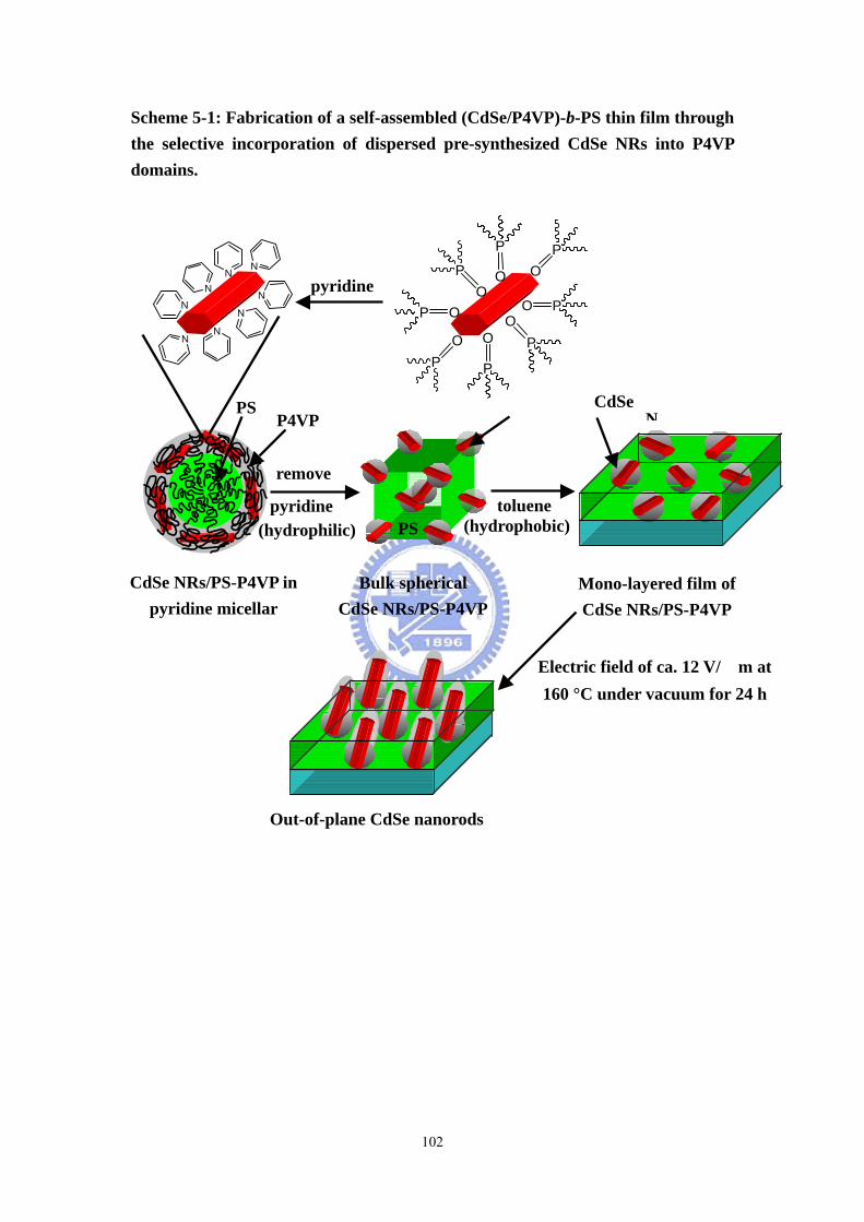
102
Scheme 5-1: Fabrication of a self-assembled (CdSe/P4VP)-b-PS thin film through the selective incorporation of dispersed pre-synthesized CdSe NRs into P4VP domains.
CdSe NRs/PS-P4VP in pyridine micellar
Bulk spherical CdSe NRs/PS-P4VP
Mono-layered film of CdSe NRs/PS-P4VP
pyridine
remove
toluene
CdSe NPS
P4VP
PS(hydrophilic) (hydrophobic)
pyridineN
N
N
N
N
N
N
N
O
P
O P
O
P
OP
OP
OP
OP
OP
Out-of-plane CdSe nanorods
Electric field of ca. 12 V/μm at 160 °C under vacuum for 24 h

103
Table 5-1: Electron barrier heights ( eφ ), electron mobilities ( 0µ ), and field coefficients ( 0E ) for in-plane and out-of-plane CdSe NRs incorporated within P4VP nanodomains in a PS matrix.
In-plane Out-of-plane vol% of CdSe in P4VP
eφ × ( ) 31
*−
mm
(eV) 0µ ×10 4
(cm2/Vs)0E ×10–4
(V/cm) eφ × ( ) 3
1*
−mm
(eV) 0µ ×10 4
(cm2/Vs) 0E ×10–4
(V/cm)
33 1.66 1.2 5.8 1.45 9.3 6.2 40 1.54 4.1 5.6 1.35 32.3 5.8 48 1.43 17.6 6.1 1.21 141.5 5.6 55 1.37 31.1 5.9 1.16 248.4 6.3 65 1.29 90.2 5.7 1.05 723.2 5.9
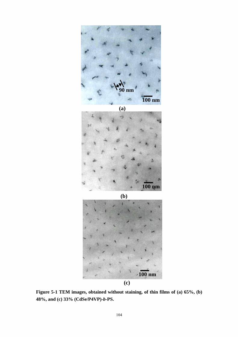
104
Figure 5-1 TEM images, obtained without staining, of thin films of (a) 65%, (b) 48%, and (c) 33% (CdSe/P4VP)-b-PS.
100 nm
(b)
(c) 100 nm
(a) 100 nm
90 nm
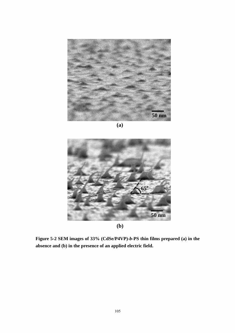
105
Figure 5-2 SEM images of 33% (CdSe/P4VP)-b-PS thin films prepared (a) in the absence and (b) in the presence of an applied electric field.
(a)
50 nm
(b)
50 nm
65o
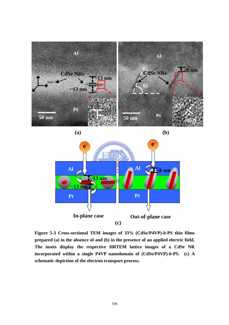
106
Figure 5-3 Cross-sectional TEM images of 33% (CdSe/P4VP)-b-PS thin films prepared (a) in the absence of and (b) in the presence of an applied electric field. The insets display the respective HRTEM lattice images of a CdSe NR incorporated within a single P4VP nanodomain of (CdSe/P4VP)-b-PS. (c) A schematic depiction of the electron transport process.
(002)
3.5A
(b)
50 nm Pt
Al
CdSe NRs
65°
(002)
3.5A
~8 nm
(a)
50 nm Pt
Al
CdSe NRs
3.5A
(002)
~13 nm
~13 nm
(c) Out-of-plane case
e-
Al
Pt
~8 nm
In-plane case
e-
Al
Pt
~13 nm ~13 nm
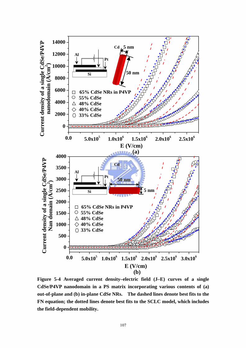
107
Figure 5-4 Averaged current density–electric field (J–E) curves of a single CdSe/P4VP nanodomain in a PS matrix incorporating various contents of (a) out-of-plane and (b) in-plane CdSe NRs. The dashed lines denote best fits to the FN equation; the dotted lines denote best fits to the SCLC model, which includes the field-dependent mobility.
0.0 5.0x10⁵ 1.0x10⁶ 1.5x10⁶ 2.0x10⁶ 2.5x10⁶ 3.0x10⁶
0
500
1000
1500
2000
2500
3000
3500
4000
E (V/cm)
Cur
rent
den
sity
of a
sing
le C
dSe/
P4V
P N
an d
omai
n (A
/cm
2 )
PtAl
Cd
Si
65% CdSe NRs in P4VP 55% CdSe 48% CdSe 40% CdSe 33% CdSe
5 nm
50 nm
0.0 5.0x10⁵ 1.0x10⁶ 1.5x10⁶ 2.0x10⁶ 2.5x10⁶
0
2000
4000
6000
8000
10000
12000
14000
E (V/cm)
Cur
rent
den
sity
of a
sing
le C
dSe/
P4V
P na
nodo
mai
n (A
/cm
2 )
PtAl
Cd
Si
65% CdSe NRs in P4VP 55% CdSe 48% CdSe 40% CdSe 33% CdSe
50 nm
5 nm
(a)
(b)
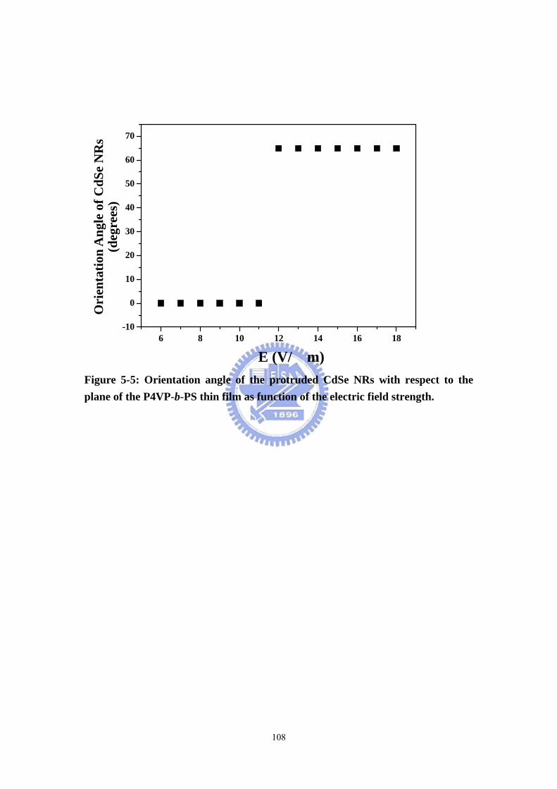
108
Figure 5-5: Orientation angle of the protruded CdSe NRs with respect to the plane of the P4VP-b-PS thin film as function of the electric field strength.
6 8 10 12 14 16 18-10
0
10
20
30
40
50
60
70
E (V/μm)
Ori
enta
tion
Ang
le o
f CdS
e N
Rs
(deg
rees
)
109
Chapter 6 Conclusions
In the (CdSe QDs/P4VP)-b-PS case, we have demonstrated that the electron
tunneling rate constant in the case of CdSe QDs confined in a P4VP nanodomain is
much larger than in the randomly distributed case and it increases upon increasing the
amount of CdSe. The value of electron tunneling coefficient of the
CdSe-P4VP-CdSe system is 0.3 A–1. The electron barrier height from the tip of the
probe to the nanodomain decreased monotonically and the conductivity of the
CdSe/P4VP nanodomain increased, following a percolation model, as the amount of
CdSe increased.
In the (Au NPs/P4VP)-b-PS case, we have demonstrated that the collective
electron transport behavior between Au NPs confined within a single P4VP
nanodomain is quasi one-dimensional, as opposed to the three-dimensional behavior
displayed by Au NPs in homo-P4VP. The threshold voltage of these composite
increased linearly upon increasing the inter-nanoparticle distance for both the
nanodomain-confined and randomly distributed samples.
In the (CdSe NRs/P4VP)-b-PS case, we have aligned CdSe nanorods that
self-assembled in the P4VP nanodomains of a PS-b-P4VP diblock copolymer thin
film through the use of polarization forces created by an applied electric field. The
electron mobilities of the CdSe/P4VP nanodomains in the out-of-plane cases were ca.
eight times larger than those in the in-plane cases. In both in the out-of-plane and
in-plane cases, the electron mobility increased upon increasing the number of CdSe
nanorods. The height of the electron barrier from the Al electrode to the
nanodomain in the out-of-plane case was much smaller than that in the in-plane case;
in both the out-of-plane and in-plane cases, the barrier height decreased upon
increasing the number of CdSe nanorods.
110
Chapter 7 References
[1] F. S. Bates and G. H. Fredrickson Annu. Rev. Phys. Chem. 1990, 41, 525.
[2] I. W. Hamley The Physics of Block Copolymers (Oxford: Oxford University Press)
1998.
[3] N. Hadjichristidis, S. Pispas and G. Floudas Block Copolymers. Synthetic
Strategies, Physical Properties and Applications (New York: Wiley), 2003.
[4] M. W. Matsen J. Phys.: Condens. Matter 2001, 14, R21.
[5] I. W. Hamley J. Phys.: Condens. Matter 2001, 13, R643.
[6] F. S. Bates and G. H. Fredrickson Phys. Today 1999, 52, 32.
[7] F. Drolet and G. H. Fredrickson Phys. Rev. Lett. 1999, 83, 4317.
[8] M. Lazzari, M. A. Lopez-Quintela Adv. Mater. 2003, 15, 1583.
[9] C. Park, J. Yoon, E. L. Thomas Polymer 2003, 44, 6725.
[10] M. Park, C. Harrison, P. M. Chaikin, R. A. Register and D. H. Adamson Science
1997, 276, 1401.
[11] C. Harrison, M. Park, P. M. Chaikin, R. A. Register and D. H. Adamson J. Vac.
Sci. Technol. B 1998, 16, 544.
[12] C. Harrison, M. Park, R. A. Register, D. Adamson, P. Mansky and P. M. Chaikin
US Patent Specification 1999, 5948470.
[13] M. Park, P. M. Chaikin, R. A. Register and D. H. Adamson Appl. Phys. Lett.
2001, 79, 257.
[14] J. Y. Cheng, C. A. Ross, V. Z.-H. Chan, E. L. Thomas, R. G. H. Lammertink and
G. J. Vancso Adv. Mater. 2001, 13, 1174.
[15] T. Thurn-Albrecht, J. Schotter, G. A. K¨astle, N. Emley, T. Shibauchi, L.
Krusin-Elbaum, K. Guarini, C. T. Black, M. T. Tuominen and T. P. Russell
Science 2000, 290, 2126.
[16] E. Jeoung, T. H. Galow, J. Schotter, M. Bal, A. Ursache, M. T. Tuominen, C. M.
111
Stafford, T. P. Russell and V. M. Rotello Langmuir 2001, 17, 6396.
[17] K. Liu, S. M. Baker, M. Tuominen, T. P. Russell and I. K. Schuller Phys. Rev. B
2001, 63, 060403(R).
[18] S. W. Yeh, K. H. Wei, Y. S. Sun, U. S. Jeng, K. S. Liang, Macromolecules 2005,
38, 6559.
[19] C. C. Weng and K. H. Wei, Chem. Mater, 2003, 15, 2936.
[20] S. W. Yeh, K. H. Wei, Y. S. Sun, U. S. Jeng, K. S. Liang, Macromolecules 2003,
36, 7903.
[21] U. S. Jeng, Y. S. Sun, H. Y. Lee, C. H. Hsu, and K. S. Liang, S. W. Yeh, K. H.
Wei, Macromolecules 2004, 37, 4617.
[22] S. W. Yeh, Y. T. Chang, C. H. Chou and K. H. Wei, Macromolecular Rapid
Communications 2004, 25, 1679.
[23] S. W. Yeh, T. L. Wu, K. H. Wei, Y. S. Sun, and K. S. Liang, J. Polym. Sci. B
Polym. Phys. 2005, 43, 1220.
[24] S. W. Yeh, T. L. Wu and K. H. Wei, Nanotechnology 2005, 16, 683.
[25] Y. Lin, A. Boker, J. He, K. Sill, H. Xiang, C. Abetz, X. Li, J. Wang, T. Emrick, S.
Long, Q. Wang, A. Balazs, T. P. Russell Nature 2005, 434, 55.
[26] M. R. Bockstaller, Y. Lapetnikov, S. Margel, E. L. Thomas J. Am. Chem. Soc.
2003, 125, 5276.
[27] J. J. Chiu, B. J. Kim, E. J. Kramer, D. J. Pine, J. Am. Chem. Soc. 2005, 127,
5036.
[28] S. Forster and M. Antonietti Adv. Mater. 1998, 10, 195.
[29] R. E. Cohen Curr. Opin. Solid State Mater. Sci. 1999, 4, 587.
[30] M. V. Seregina, L. M. Bronstein, O. A. Platonova, D. M. Chernyshov, P. M.
Valetsky, J. Hartmann, E. Wenz and M. Antonietti Chem. Mater. 1997, 9, 923.
[31] L. M. Bronstein, S. N. Sidorov, P. M. Valetsky, J. Hartmann, H. C¨olfen and M.
112
Antonietti Langmuir 1999, 15, 6256.
[32] M. Antonietti, E. Wenz, L. Bronstein and M. Seregina Adv. Mater. 1995, 7,
1000.
[33] O. A. Platonova, L. M. Bronstein, S. P. Solodovnikov, I. M. Yanovskaya, E. S.
Obolonkova, P. M. Valetsky, E. Wenz and M. Antonietti Colloid Polym. Sci. 1997,
275, 426.
[34] B. H. Sohn and B. H. Seo Chem. Mater. 2001, 13, 1752.
[35] J. Spatz, S. Mossmer, M. Moller, M. Kocher, D. Neher and G. Wegner Adv.
Mater. 1998, 10, 473.
[36] C. C. Weng, K. F. Hsu and K. H. Wei, Chem. Mater. 2004, 16, 4080.
[37] A. C. Edrington Adv. Mater. 2001, 13, 421.
[38] Y. Fink, A. M. Urbas, M. G. Bawendi, J. D. Joannopoulos and E. L. Thomas J.
Lightwave Technol. 1999, 17, 1963.
[39] M. Maldovan, A. M. Urbas, N. Yufa, W. C. Carter and E. L. Thomas Phys. Rev.
B 2002, 65, 165123.
[40] A. M. Urbas, M. Maldovan, P. DeRege and E. L. Thomas Adv. Mater. 2002, 14,
1850.
[41] T. Hashimoto, K. Tsutsumi and Y. Funaki Langmuir 1997, 13, 6869.
[42] A. P. Alivisatos, Endeavour 1997, 21, 56.
[43] M. A. El-Sayed, M. Acc. Chem. Res. 2004, 37, 326.
[44] H. S. Naiwa, Hitachi Research lab. In Handbook of Nanostructure Materials and
nanotechnology v4. Chapter 5, 2000.
[45] Y. Wang and N. Herron J. Phys. Chem. 1991, 95, 525.
[46] J. T. Hu, L. S. Li, W. D. Yang, L. Manna, L. W. Wang and A. P. Alivisatos
Science 2001, 292, 2060.
[47] X. Chen, A. Nazzal, D. Goorskey, M. Xiao, Z. A. Peng and X. Peng Phys. Rev. B
113
2001, 64, 5304.
[48] M. Kazes, D. Y. Lewis, Y. Ebenstein, T. Mokari and U. Banin Adv. Mater. 2002,
14, 317.
[49] D. Katz, T. Wizansky, O. Millo, E. Rothenberg, T. Mokari and U. Banin Phys.
Rev. Lett. 2002, 89, 86801.
[50] C. B. Murray, D. J. Norris, M. G. Bawendi, J. Am. Chem. Soc. 1993, 115, 8706.
[51] M. C. Schlamp, X. G. Peng, A. P. Alivisatos J. Appl. Phys. 1997, 82, 5837.
[52] W. Huynh, J. J. Dittmer, A. P. Alivisatos Science 2002, 295, 2425.
[53] V. I. Klimov, A. A. Mikhailovsky, S. Xu, A. Malko, J. A. Hollingsworth, C. A.
Leatherdale, H. J. Eisler, M. G. Bawendi Science 2000, 290, 314.
[54] M. P. Bruchez, M. Moronne, P. Gin, S. Weiss, A. P. Alivisatos Science 1998, 281,
2013.
[55] A. P. Alivisatos Science 1996, 271, 933.
[56] M. Brust, C. J. Kiely Colloids Surf. A: Physicochem. Eng. Asp. 2002, 202, 175.
[57] R. P. Andres, T. Bein, M. Dorogi, S. Feng, J. I. Jenderson, C. P. Kubiak, W.
Mahoney, R. G. Osifchin, R. Reifenverger Science 1996, 272, 1323.
[58] J. Ouyang, C. –W. Chu, D. Sieves, Y. Yang Appl. Phys. Lett. 2005, 86, 123507.
[59] U. Simon Adv. Mater. 1998, 10, 1487.
[60] T. Sato, H. Ahmed, D. Brown, B. F. H. Johnson, J. Appl. Phys. 1997, 82, 696.
[61] C. A. Mirkin, T. A. Taton Nature 2000, 405, 626.
[62] A. P. Alivisatos, K. P. Johnsson, X. Peng, T. E. Wislon, C. J. Loweth, M. P.
Bruchez, P. G. Schultz Nature 1996, 382, 609.
114
[63] A. Ueda, T. Oshima, M. Haruta Appl. Catal. B 1997, 12, 81.
[64] A. A. Middletion, N. S. Wingreen Phys. Rev. Lett. 1993, 71, 3198.
[65] U. Geigenmuller, G. Schon, Europhys. Lett. 1989, 10, 765.
[66] H. Fan, K. Yang, D. M. Boye, T. Sigmon, K. J. Malloy, H. Xu, G. P. López, C. J.
Brinker Science 2004, 304, 567.
[67] C. T. Black, C. B. Murray, R. L. Sandstrom, S. Sun Science 2000, 290, 1131.
[68] S. Datta, W. Tian, S. Hong, R. Reifenberger, J. Henderson, C. P. Kubiak, Phys.
Rev. Lett. 1997, 79, 2530.
[69] D. R. Lamb, “Electrical Conduction Mechanisms in Thin Insulating Films”,
Methue, London, 1967.
[70] C.P. Collier, G. Mattersteig, E. W. Wong, Y. Luo, K. Beverly, J. Sampaio, F. M.
Raymo, J. F. Stoddart, and J. R. Heth, Science 2000, 289, 1171.
[71] M. A. Reed, J. Chen, A. M. Rawlett, D. W. Price, and J. M. Tour, Appl. Phys.
Lett. 2001, 78, 3735.
[72] L. A. Bumm, J. J. Arnold, T. D. Dunbar, D. L. Allara, and P. S. Weiss, J. Phys.
Chem. B 1999, 103, 8122.
[73] D. J. Wold, R. Haag, M. A. Rampi, and C. D. Frisbie, J. Phys. Chem. B 2002,
106, 2813.
[74] X. D. Cui, X. Zarate, J. Tomfohr, O. F. Sankey, A. Primak, A. L. Moore, T. A.
Moore, D. Gust, G. Harris, and S. M. Lindsay, Nanotechnology 2002, 13, 5.
[75] R. Holmlin, R. Haag, M. L. Chabinyc, R. F. Ismagilov, A. E. Cohen, A. Terfort,
M. A. Rampi, and G. M. Whitesides, J. Am. Chem. Soc. 2001, 123, 5075.
[76] M. P. Samanta, W. Tian, S. Datta, J. I. Henderson, and C. P. Kubiak, Phys. Rev.
B 1996, 53, R7636.
[77] G. H. Parker and C. A. Mead, Phys. Rev. Lett. 1968, 21, 605.
[78] B. Brar, G. D. Wilk, and A. C. Seabaugh, Appl. Phys. Lett. 1996, 69, 2728.
115
[79] X. D. Cui, A. Primak, X. Zarate, J. Tomfohr, O. F. Sankey, A. L. Moore, T. A.
Moore, D. Gust, L. A. Nagahara, and S. M. Lindsay, J. Phys. Chem. B 2002, 106,
8609.
[80] Although the HOMO-LUMO gap of alkyl chain type molecules has been
reported (see references [92]), there is no experimental data on HOMO-LUMO
gap for Au/alkanethiol SAM/Au system. 8 eV is commonly used as
HOMO-LUMO gap of alkanethiol.
[81] C. Boulas, J. V. Davidovits, F. Rondelez, and D. Vuillaume, Phys. Rev. Lett.
1996, 76, 4797.
[82] W. Huynh, J. J. Dittmer, A. P. Alivisatos, Science 2002, 295, 2425.
[83] H. Fan, K.Yang, D. M. Boye, T. Sigmon, K. J. Malloy, H. Xu, G. P. López, C. J.
Brinker, Science 2004, 304, 567.
[84] a) A. L. Roest, J. J. Kelly, D. Vanmaekelbergh Phys. Rev. Lett. 2002, 89, 036801;
b) A. L. Roest, J. J. Kelly, D. Vanmaekelbergh Appl. Phys. Lett. 2003, 83, 5530.
[85] D. Yu, C. Wang, P. Guyot-Sionnest, Science 2003, 300, 1277.
[86] W. P. Wuelfing, S. J. Green, J. J. Pietron, D. E. Cliffel, R. W. Murry, J. Am. Chem.
Soc. 2000, 122, 11465.
[87] R. J. Forster, L.Keane, J. Electroanal. Chem. 2003, 554-555, 345.
[88] E. P. A. M. Bakkers, A. W. Marsman, L. W. Jenneskens, D. Vanmaekelbergh,
Angew. Chem. 2000, 112, 2385-2388; Angew. Chem. Int. Ed. 2000, 39, 2297.
[89] E. P. A. M. Bakkers, Z. Hens, A. Zunger, A. Franceschetti, L. P. Kouwenhoven, L.
Gurevich, D. Vanmaekelbergh, Nano Lett. 2001, 1, 551.
[90] J. P. Spatz, S. Mossmer, C. Hartmann, M. Möller, T. Herzog, M. Krieger, H. G.
Boyen, P. Ziemann, B. Kabius, Langmuir 2000, 16, 407.
[91] a) C. C. Weng, K. H. Wei, Chem. Mater. 2003, 15, 2936; b) C. C. Weng, C. P.
116
Chen; C. H. Ting; K. H. Wei, Chem. Mater. 2005, 17, 3328.
[92] Y. Lin, A. Böker, J. He, K. Sill, H. Xiang, C. Abetz, X. Li, J. Wang, T. Emrick, S.
Long, Q. Wang, A. Balazs, T. P. Russell, Nature 2005, 434, 55.
[93] Y. Kang, T. A. Taton, Angew. Chem. 2005, 117, 413.; Angew. Chem. Int. Ed. 2005,
44, 409.
[94] N. Tesster, V. Medvedev, M. Kazes, S. Kan, U. Banin, Science 2002, 295, 1506.
[95] X. D. Cui, X. Zarate, J. Tomfohr, O. F. Sankey, A. Primak, A. L. Moore, T. A.
Moore, D. Gust, G. Harris, S. M. Lindsay, Nanotechnology 2002, 13, 5.
[96] F. P. Zamborini, L. E. Smart, M. C. Leopold, R. W. Murry, Anal. Chim. Acta
2003, 496, 3.
[97] a) A. Salomon, D. Cahen, S. Lindsay, J. Tomfohr, V. B. Engelkes, C. D. Frisbie,
Adv. Mater 2003, 15, 1881; b) X. D. Cui, X. Zarate, J. Tomfohr, O. F. Sankey, A.
Primak, A. L. Moore, T. A. Moore, D. Gust, G. Harris, S. M. Lindsay,
Nanotechnology 2002, 13, 5.
[98] N. Boden, R. J. Bushby, J. Clements, B. Movaghar, J. Appl. Phys 1998, 83, 3207.
[99] We measured the HOMO and LUMO states of P4VP through the use of cyclic
voltammetry (CV).
[100] Z. A. Peng, X. Peng, J. Am. Chem. Soc. 2001, 123, 183.
[101] a) D. Xu, G. D. Watt, J. N. Harb, R. C. Davis Nano Lett. 2005, 5, 571; b) Y.
Kawabe, M. M. Morrell, G. E. Jabbour, S. E. Shahen, B. Kippelen, J. Appl. Phys
1998, 84, 5306.
[102] C. I. Zanetti, A. Mechler, S.A. Carter, R. Lal, Adv. Mater. 2004, 16, 385.
[103] We calculated the concentration of CdSe in the P4VP domain (mol/cm3) from
117
the loading amount of CdSe in P4VP. The value of C obtained by dividing the
entire mole of CdSe by the entire volume of P4VP.
[104] W. J. Parak, T. Pellegrino, C. M. Micheel, D. Gerion, S. C. Williams, A. P.
Alivisatos, Nano Lett. 2003, 3, 33.
[105] M. Brust, M. Walker, D. Bethell, D. J. Schiffrin, R. Whyman, J. Chem. Soc.
Chem. Commun. 1994, 801.
[106] C. B. Murray, C. R. Kagan, M. G. Bawendi Annu. Rev. Mater. Sci. 2000, 30,
545.
[107] J. Ouyang, C. –W. Chu, D. Sieves, Y. Yang, Appl. Phys. Lett. 2005, 86, 123507.
[108] U. Simon Adv. Mater. 1998, 10, 1487.
[109] C. A. Mirkin, T. A. Taton, Nature 2000, 405, 626.
[110] A. Ueda, T. Oshima, M. Haruta Appl. Catal. B 1997, 12, 81.
[111] C. P. Collier, R. J. Saykally, J. J. Shiang, S. E. Henrichs, J. R. Heath, Science
1997, 277, 1978.
[112] R. Parthasarathy, X. M. Lin, H. M. Jaeger Phys. Rev. Lett. 2001, 87, 186807.
[113] H. Fan, K. Yang, D. M. Boye, T. Sigmon, K. J. Malloy, H. Xu, G. P. López, C. J.
Brinker Science 2004, 304, 567.
[114] C. T. Black, C. B. Murray, R. L. Sandstrom, S. Sun Science 2000, 290, 1131.
[115] P. Beecher, A. J. Quinn, E. V. Shevchenko, H. Weller, G. Redmond J. Phys.
Chem. B 2004, 108, 9564.
[116] a) W. P. Wuelfing, S. J. Green, J. J. Pietron, D. E. Cliffel, R. W. Murry, J. Am.
Chem. Soc. 2000, 122, 11465. b) W. P. Wuelfing, R. W. Murry, J. Phys. Chem. B
2002, 106, 3139.
[117] E. P. A. M. Bakkers, A. W. Marsman, L. W. Jenneskens, D. Vanmaekelbergh,
Angew. Chem. Int. Ed. 2000, 39, 2297.
[118] a) Y. Lin, A. Böker, J. He, K. Sill, H. Xiang, C. Abetz, X. Li, J. Wang, T. Emrick,
118
S. Long, Q. Wang, A. Balazs, T. P. Russell, Nature 2005, 434, 55. b) Q. Zhang, S.
Gupta, T. Emrick, T. P. Russell, J. Am. Chem. Soc. 2005, 128, 3898.
[119] a) B. J. Kim, J. J. Chiu, G. –R. Yi, D. J. Pine, E. J. Kramer, Adv. Mater. 2005,
17, 2618. b) J. J. Chiu, B. J. Kim, E. J. Kramer, D. J. Pine, J. Am. Chem. Soc. 2005,
127, 5036.
[120] T. Ruotsalainen, J. Turku, P. Heikkilä, J. Roukolainen, A. Nykänen, T. Laitinen,
M. Torkkeli, R. Serimaa, G. T. Brinke, A. Harlin, O. Ikkala, Adv. Mater. 2005, 17,
1048.
[121] A. M. Urbas, M. Maldovan, P. DeRege, E. L. Thomas, Adv. Mater. 2002, 14,
1850.
[122] a) C. P. Li, K. H. Wei, J. Y. Huang, Angew. Chem. Int. Ed. 2006, 45, 1449. b) C.
P. Li, S. W. Yeh, H. C. Chang, J. Y. Huang, K. H. Wei, Small 2006, 2, 359.
[123] a) J. P. Spatz, S. Mossmer, C. Hartmann, M. Möller, T. Herzog, M. Krieger, H.
G. Boyen, P. Ziemann, B. Kabius, Langmuir 2000, 16, 407. b) J. P. Spatz, V. Z. H.
Chan, S. Mößmer, F. –M. Kamm, A. Plettl, P. Ziemann, M. Möller, Adv. Mater.
2002, 14, 1827.
[124] A. A. Middleton, N. S. Wingreen, Phys. Rev. Lett. 1993, 71, 3198.
[125] C. A. Neugebauer, M. B. Webb, J. Appl. Phys. 1962, 33, 74.
[126] In two- and three-dimensional hexagonal arrays, each nanoparticle has six and
twelve nearest neighbors, respectively.
[127] a) J. W. Grebinski, K. L. Richter, J. Zhang, T. H. Kosel, M. Kuno, J. Phys.
Chem. B 2004, 108, 9745. b) W. W. Weare, S. M. Reed, M. G. Warner, J. E.
Hutchison, J. Am. Chem. Soc. 2000, 122, 12890.
[128] a) W. P. Wuelfing, S. J. Green, J. J. Pietron, D. E. Cliffel, R. W. Murry, J. Am.
Chem. Soc. 2000, 122, 11465. b)F. P. Zamborini, L. E. Smart, M. C. Leopold, R.
W. Murry, Anal. Chim. Acta 2003, 496, 3.
119
[129] a) T. Ruotsalainen, J. Turku, P. Heikkilä, J. Roukolainen, A. Nykänen, T.
Laitinen, M. Torkkeli, R. Serimaa, G. T. Brinke, A. Harlin, O. Ikkala, Adv. Mater.
2005, 17, 1048–1052; b) S. Valkama, H. Kosonen, J. Ruokolainen, T. Haatainen,
M. Torkkeli, R. Serimaa, G. T. Brinke, O. Ikkala, Nature Mater. 2004, 3, 872.
[130] a) M. Park, C. Harrison, P. M. Chaikin, R. A. Register, D. H. Adamson, Science
1997, 267, 1401; b) Y. L. Loo, R. A. Register, A. J. Ryan, Macromolecules 2002,
35, 2365.
[131] a) M. J. Misner, H. Skaff, T. Emrick, T. P. Russell, Adv. Mater. 2003, 15, 221;
b) D. H. Kim, S. H. Kim, K. Lavery, T. P. Russell, Nano Lett. 2004, 4, 1841; c)
Y. Lin, A. Böker, J. He, K. Sill, H. Xiang, C. Abetz, X. Li, J. Wang, T. Emrick, S.
Long, Q. Wang, A. Balazs, T. P. Russell, Nature 2005, 434, 55.
[132] a) A. M. Urbas, M. Maldovan, P. DeRege, E. L. Thomas, Adv. Mater. 2002, 14,
1850; b) M. Bockstaller, R. Olb, E. L. Thomas, Adv. Mater. 2001, 13, 1783.
[133] a) J. P. Spatz, S. Mossmer, C. Hartmann, M. Möller, T. Herzog, M. Krieger, H.
G. Boyen, P. Ziemann, B. Kabius, Langmuir 2000, 16, 407; b) J. P. Spatz, V. Z.-H.
Chan, S. Mößmer, F.-M. Kamm, A. Plettl, P. Ziemann, M. Möller, Adv. Mater.
2002, 14, 1827.
[134] S. W. Yeh, K. H. Wei, Y. S. Sun, U. S. Jeng, K. S. Liang, Macromolecules 2005,
38, 6559.
120
[135] a) X. Duan, Y. Huang, R. Agarwal, C. M. Lieber, Nature 2003, 421, 241; b) Y.
Cui, Q. Wei, H. Park, C. M. Lieber, Science 2001, 293, 1289.
[136] L. K. vanVugt, S. J. Veen, E. P. A. M. Bakkers, A. L. Roest, D. Vanmaekelbergh,
J. Am. Chem. Soc. 2005, 127, 13257.
[137] M. Artemyev, B. Möller, U. Woggon, Nano Lett. 2003, 3, 509.
[138] F. Kim, S. Kwan, J. Akana, P. Yang, J. Am. Chem. Soc. 2001, 123, 4360.
[139] a) W. U. Huynh, J. J. Dittmer, A. P. Alivisatos, Science 2002, 295, 2425; b) J.
Hu, L. S. Li, W. Yang, L. Manna, L. W. Wang, A. P. Alivisatos, Science 2001, 292,
2060; c)L. S. Li, A. P. Alivisatos, Adv. Mater. 2003, 15, 408.
[140] Y. W. Su, C. S. Wu, C. C. Chen, C. D. Chen, Adv. Mater. 2003, 15, 49.
[141] M. H. Huang, S. Mao, H. Feick, H. Yan, Y. Wu, H. Kind, E. Weber, R. Russo, P.
Yang, Science 2001, 292, 1897.
[142] a) O. Harnack, C. Pacholski, H. Weller, A. Yasuda, J. M. Wessels, Nano Lett.
2003, 3, 1097; b) P. A. Smith, C. D. Nordquist, T. N. Jackson, T. S. Mayer, B. R.
Martin, J. Mbindyo, T. E. Mallouk, Appl. Phys. Lett. 2000, 77, 1399.
[143] R. A. Mrozek, T. A. Taton, Chem. Mater. 2005, 17, 3384.
[144] a) T. Xu, A. V. Zvelindovsky, G. J. A. Sevink, O. Gang, B. Ocko, Y. Zhu, S. P.
Gido, T. P. Rusell, Macromolecules 2004, 37, 6980; b) H. Xiang, Y. Lin, T. P.
Rusell, Macromolecules 2004, 37, 5358.
121
[145] H. A. Pohl, J. Appl. Phys. 1915, 22, 869.
[146] L. S. Li, A. P. Alivisatos, Phys. Rev. Lett. 2003, 90, 097402.
[147] a) D. Xu, G. D. Watt, J. N. Harb, R. C. Davis Nano Lett. 2005, 5, 571; b) Y.
Kawabe, M. M. Morrell, G. E. Jabbour, S. E. Shahen, B. Kippelen, J. Appl. Phys
1998, 84, 5306.
[148] P. W. M. Blom, M. J. M. de Jong, J. J. M. Vleggar, Appl. Phys. Lett. 1996, 68,
3308.
[149] Z. A. Peng, X. Peng, J. Am. Chem. Soc. 2002, 124, 3343.
122
Publication Lists
Chung-Ping Li, Kung-Hwa Wei and Jung Y. Huang, “Enhanced Collective Electron Transport by CdSe Quantum Dots Self-Assembled in the Poly(4-vinylpyridine) Nanodomains of a Poly(styrene-b-4-vinylpyridine) Diblock Copolymer Thin Film”, Angew. Chem. Int. Ed. 2006, 45, 1449. (Impact Factor 9.161) Chung-Ping Li, Siao-Wei Yeh, Han-Chang Chang, Jung Y. Huang, and Kung-Hwa Wei, “The Orientation of CdSe Nanorods Affects the Electron Mobility of CdSe/P4VP Nanodomains Self-Assembled within a Poly(styrene-b-4-vinylpyridine) Diblock Copolymer Thin Film”, Small 2006, 2, 359. (starts at 2005, no Impact Factor until 2007) Chung-Ping Li, Ching-Mao Huang, Meng-Ting Hsieh and Kung-Hwa Wei, “Properties of Covalently Bonded Layered-Silicate/Polystyrene Nanocomposites Synthesized via Atom Transfer Radical Polymerization”, J. Polym. Sci. Part A: Polym. Chem. 2005, 43, 534. (Impact Factor 2.773) Chung-Ping Li, Chia-Hao Wu, Kung-Hwa Wei, Jeng-Tzong Sheu, and Jung Y. Huang, “Collective Electron Transport in Au Nanoparticles Self-Assembled in the Poly(4-vinylpyridine) Nanodomains of a Poly(styrene-b-4-vinylpyridine) Diblock Copolymer Thin Film”, J. Am.Chem. Soc. 2006, submitted. (Impact Factor 6.903)

123
學經歷資料
姓名:李中斌 性別:男 生日:67年 9月 22日,台南人 電子郵件信箱:[email protected] 聯絡電話:(學校) 03-5731771 (手機) 0922-110935 通訊地址:新竹市 300大學路 1001號
國立交通大學材料與工程研究所 永久地址:台南縣麻豆鎮建南街 122巷 1號
學歷 博士候選人:國立交通大學材料科學與工程研究所 2000. 9 ~ 2006. 6 大學:國立彰化師範大學化學系 1996. 9 ~ 2000. 6 參與計畫 高效率光電轉換自身組織功能性奈米結構材料與元件之前瞻研究。(2005. 8
~ 2006. 6) 量子點/自身組織塊式高分子奈米複合材料。(2002. 1 ~ 2005. 12) 原位(In-situ)聚合之無機層狀材/聚苯乙烯(PS)奈米複合材料之製備。(2001.
8~2002. 7) 低介電溶膠凝膠聚亞醯胺(PI)奈米複合材料之製備。(2000. 9 ~ 2001. 7)
專長 光電量測與奈米操控技術:
1. 奈米區塊(nanodomain)之光電性質之量測。 2. 光電應用奈米材料操控與分散技術。 3.無機奈米結構(nanostructure)之合成、鑑定分析與其界面改質分散技術。
有機/無機奈米複合材料: 1.原位聚合奈米分散技術。 2.構裝用低介電聚亞醯(PI)與/無機物奈米複合材料。 分析儀器操作: 小角 X光散射(SAXS)、原子力顯微鏡(AFM)、掃瞄穿遂顯微鏡(STM)、穿透式電子顯微鏡(TEM)、掃瞄式電子顯微鏡(SEM)、X光繞射分析、超薄切片機、光學量測儀器、電性量測分析、紅外線光譜分析、紫外光-可見光光譜分析、熱分析(DSC, TGA, TMA)、粒徑分析、及真空蒸鍍設備操作。