課程名稱:能量擷取技術 Energy Harvesting...
77
1 課程名稱:能量擷取技術 Energy Harvesting Technologies 授課教師:王東安 Lecture 1
Transcript of 課程名稱:能量擷取技術 Energy Harvesting...

1
課程名稱:能量擷取技術Energy Harvesting Technologies
授課教師:王東安Lecture 1

2
Dung-An Wang Phone: 04-22840531 ext. [email protected]
LECTURES: Wednesdays 1:10-4pmOFFICE HOURS: Wednesdays 11am-noonCourse website: web.nchu.edu.tw/~daw/Teaching/Energy/energy_harvester.htm
TEXTBOOK: Shashank Priya and Daniel J. Inman, “Energy
Harvesting Technologies”, Springer, 2008.GRADING: Homework (30%), Midterms (20%) Project(30%)
Final (20%).HOMEWORK: Homework is due at the begging of the class.
Late homework is not accepted.

3
COURSE OBJECTIVE•Understand a systematic approach to analyzing
energy harvesting problems.•Study the techniques to design of energy harvesting
system.•Practice the systematic process on a semester-long
project.
4
Lecture Outline•Vibration energy harvesting•Electrostatic harvester•Electromagnetic harvester•Piezoelectric harvester

5
Energy Harvesting•Definition: The process of converting ambient energy
into electrical energy.•Characteristics
–Small amount of power for low-energy electronics–Energy source for energy harvesters is ambient and
free–Little power generation, order of W/cm3, need to be
stored in a capacitor or battery.•Use capacitors when huge energy spikes are needed. Batteries for a
steady flow of energy supply.
6
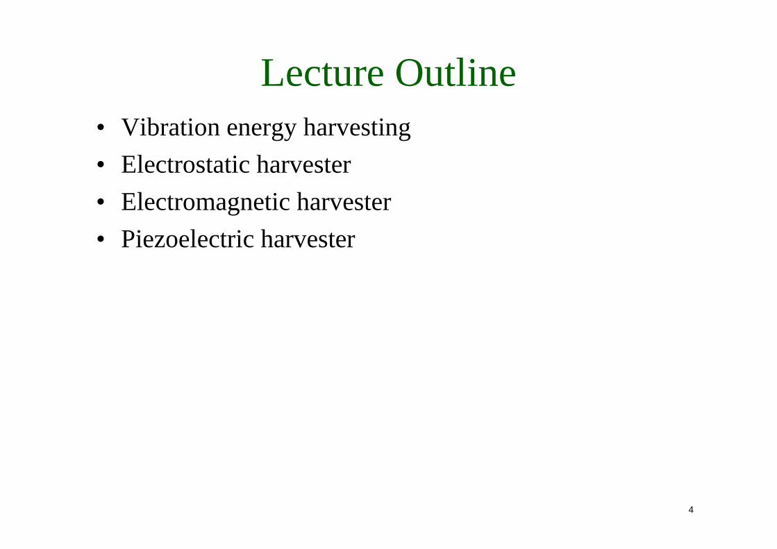
Why Harvesting Energy?•Independent sensor networks, mobile devices
–Autonomous–No maintenance–Free–Low carbon print
7
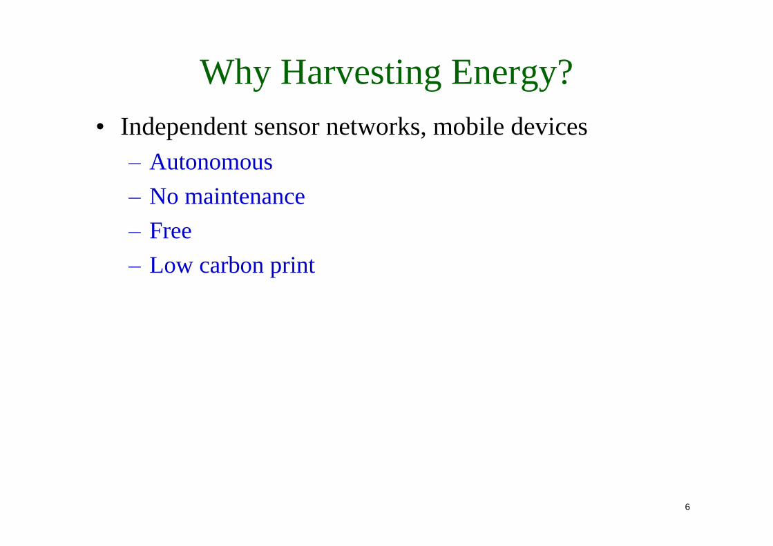
The sources•Solar power•Thermal energy•Wind energy•Salinity gradients•Vibration energy
8
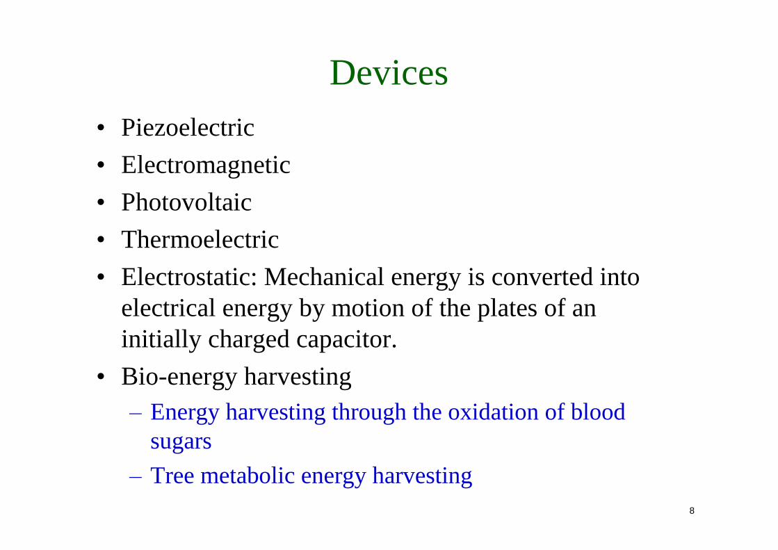
Devices•Piezoelectric•Electromagnetic•Photovoltaic•Thermoelectric•Electrostatic: Mechanical energy is converted into
electrical energy by motion of the plates of aninitially charged capacitor.
•Bio-energy harvesting–Energy harvesting through the oxidation of blood
sugars–Tree metabolic energy harvesting

9
Market perspective•The energy harvesting market has potential to
approach the $250 million mark in 2017 due todemand for wireless networks. (MEMS’s trend, Oct2012)
10
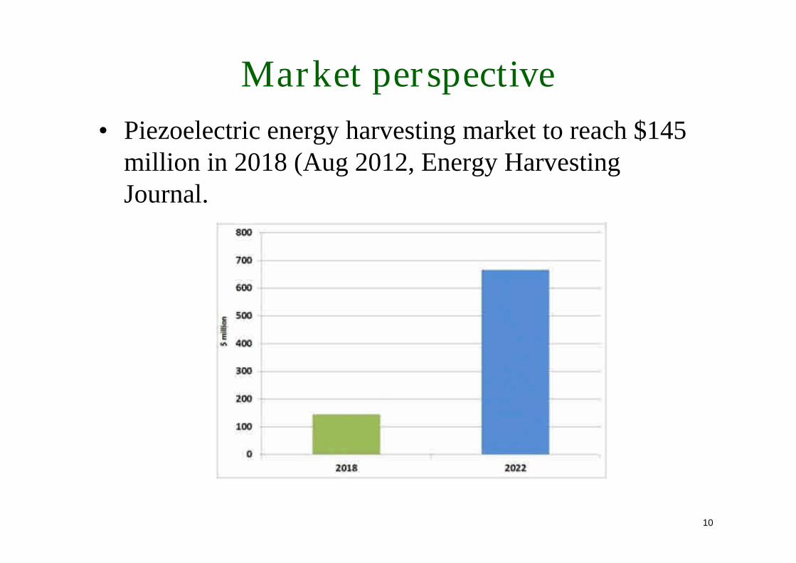
Market perspective•Piezoelectric energy harvesting market to reach $145
million in 2018 (Aug 2012, Energy HarvestingJournal.
11
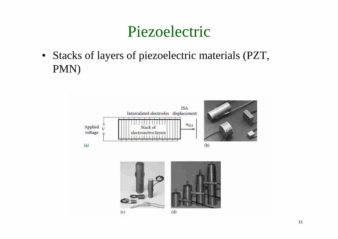
Piezoelectric•Stacks of layers of piezoelectric materials (PZT,
PMN)
12
Magnetostrictive Material (MsM)
13
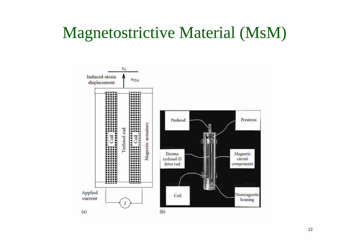
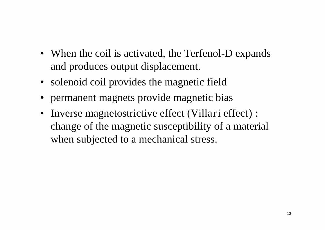
•When the coil is activated, the Terfenol-D expandsand produces output displacement.
•solenoid coil provides the magnetic field•permanent magnets provide magnetic bias•Inverse magnetostrictive effect (Villari effect) :
change of the magnetic susceptibility of a materialwhen subjected to a mechanical stress.
14
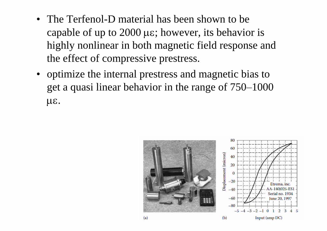
•The Terfenol-D material has been shown to becapable of up to 2000 ; however, its behavior ishighly nonlinear in both magnetic field response andthe effect of compressive prestress.
•optimize the internal prestress and magnetic bias toget a quasi linear behavior in the range of 750–1000.
15
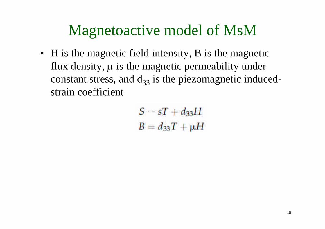
Magnetoactive model of MsM•H is the magnetic field intensity, B is the magnetic
flux density, is the magnetic permeability underconstant stress, and d33 is the piezomagnetic induced-strain coefficient
16
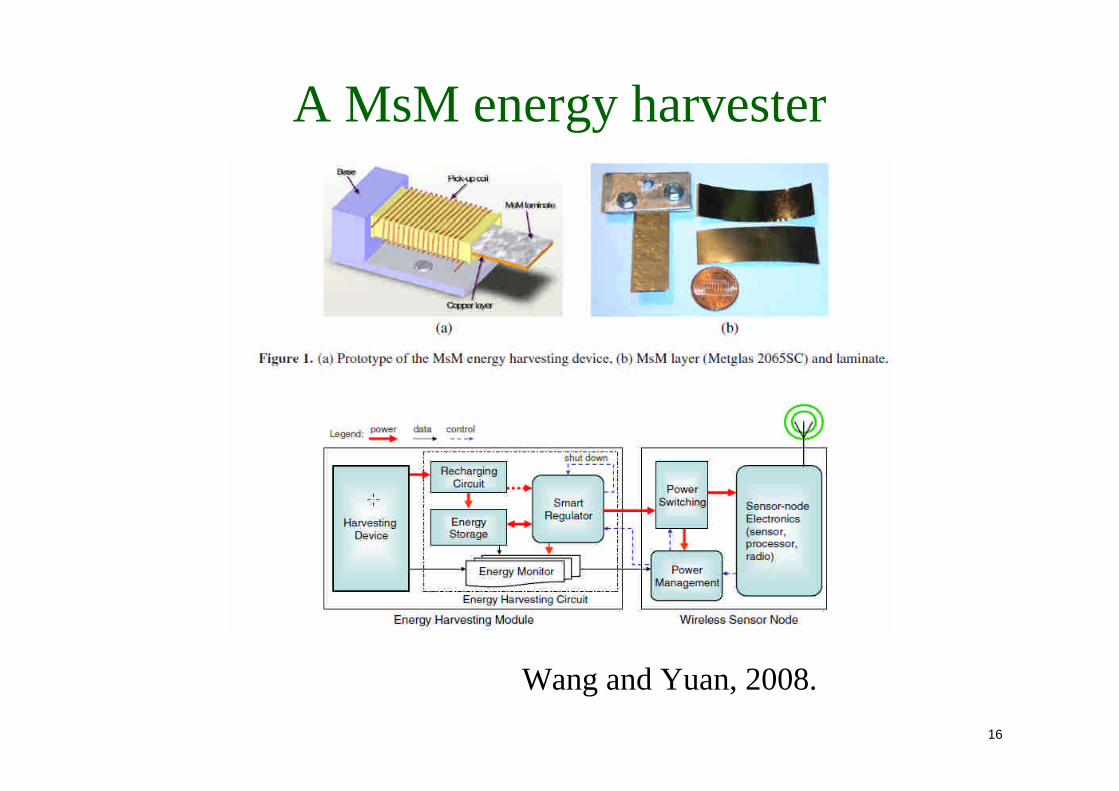
A MsM energy harvester
Wang and Yuan, 2008.

17
MsM•Upon dynamic or cyclic loading, this change in
magnetization is converted into electrical energyusing a pickup coil surrounding the MsM laminateaccording to Faraday’s law.
•One drawback of the MsM, Terfenol-D, for energyharvesting is the requirement for a bias magnetic field.

18
Electromagnetic power generators•Electromagnetic power generators (EMPGs) have the
advantages of low output impedance and high outputcurrent levels
19
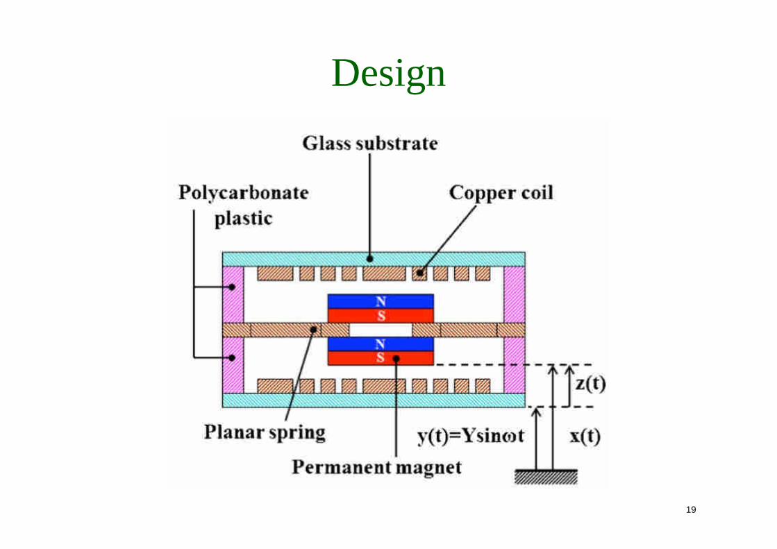
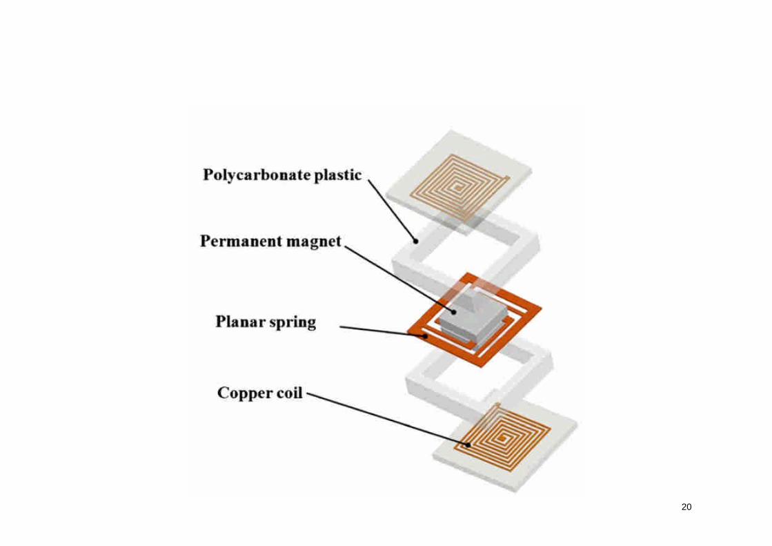
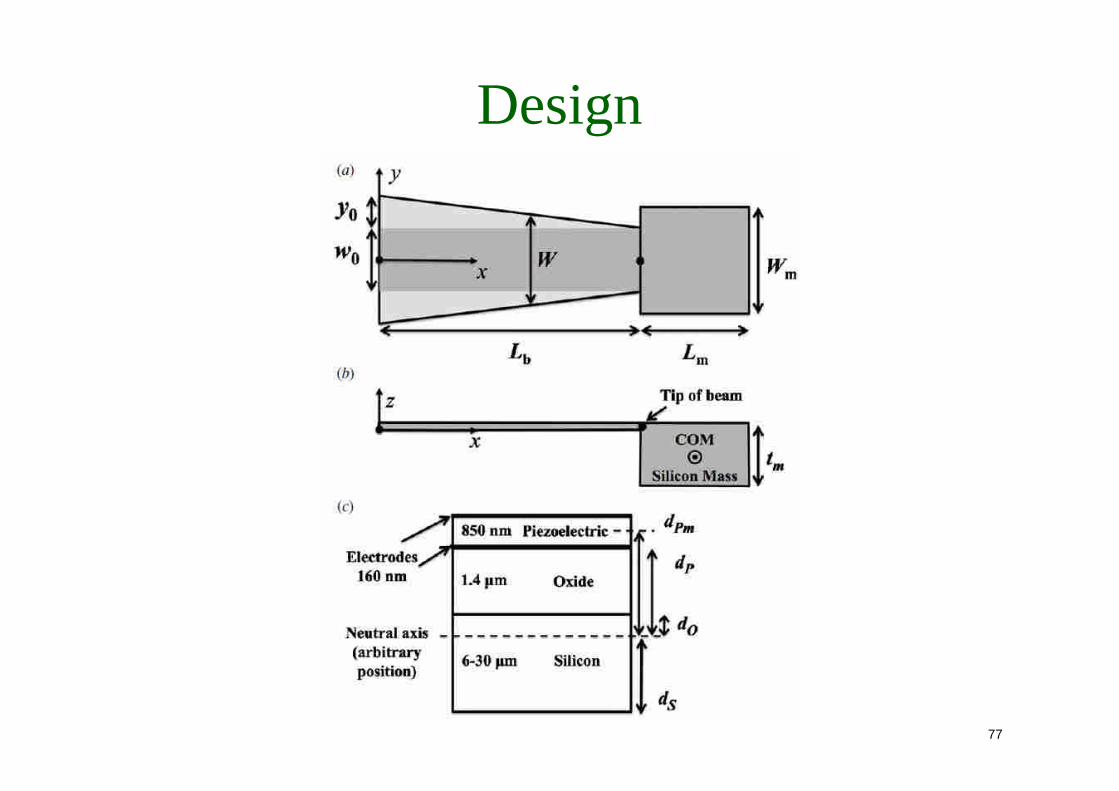
Design
20
21
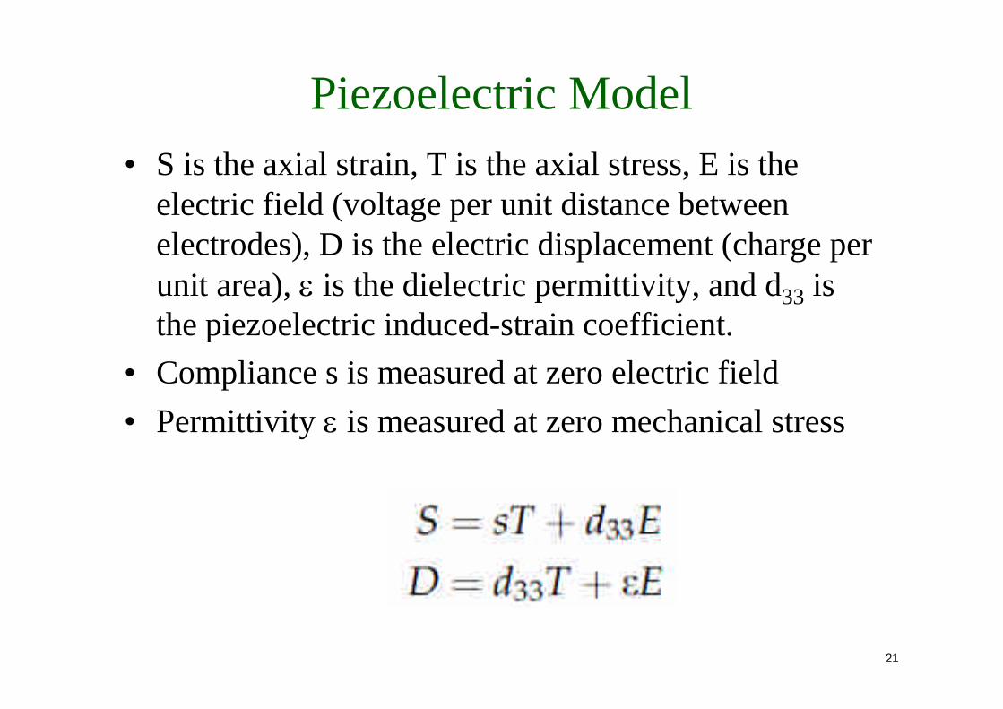
Piezoelectric Model•S is the axial strain, T is the axial stress, E is the
electric field (voltage per unit distance betweenelectrodes), D is the electric displacement (charge perunit area), is the dielectric permittivity, and d33 isthe piezoelectric induced-strain coefficient.
•Compliance s is measured at zero electric field•Permittivity is measured at zero mechanical stress
22
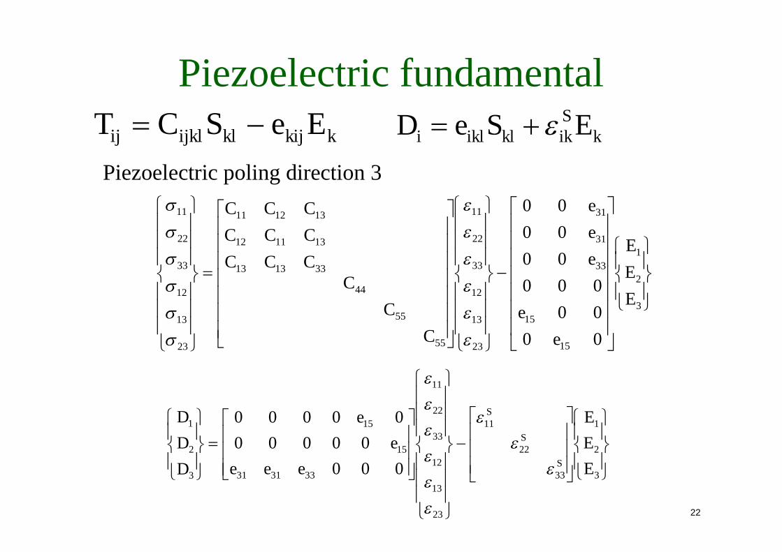
Piezoelectric fundamentalkkijklijklij EeSCT k
Sikklikli ESeD
3
2
1
15
15
33
31
31
23
13
12
33
22
11
55
55
44
331313
131112
131211
23
13
12
33
22
11
0000000
000000
EEE
ee
eee
CC
CCCCCCCCCC
3
2
1
33
22
11
23
13
12
33
22
11
333131
15
15
3
2
1
00000000
00000
EEE
eeee
e
DDD
S
S
S
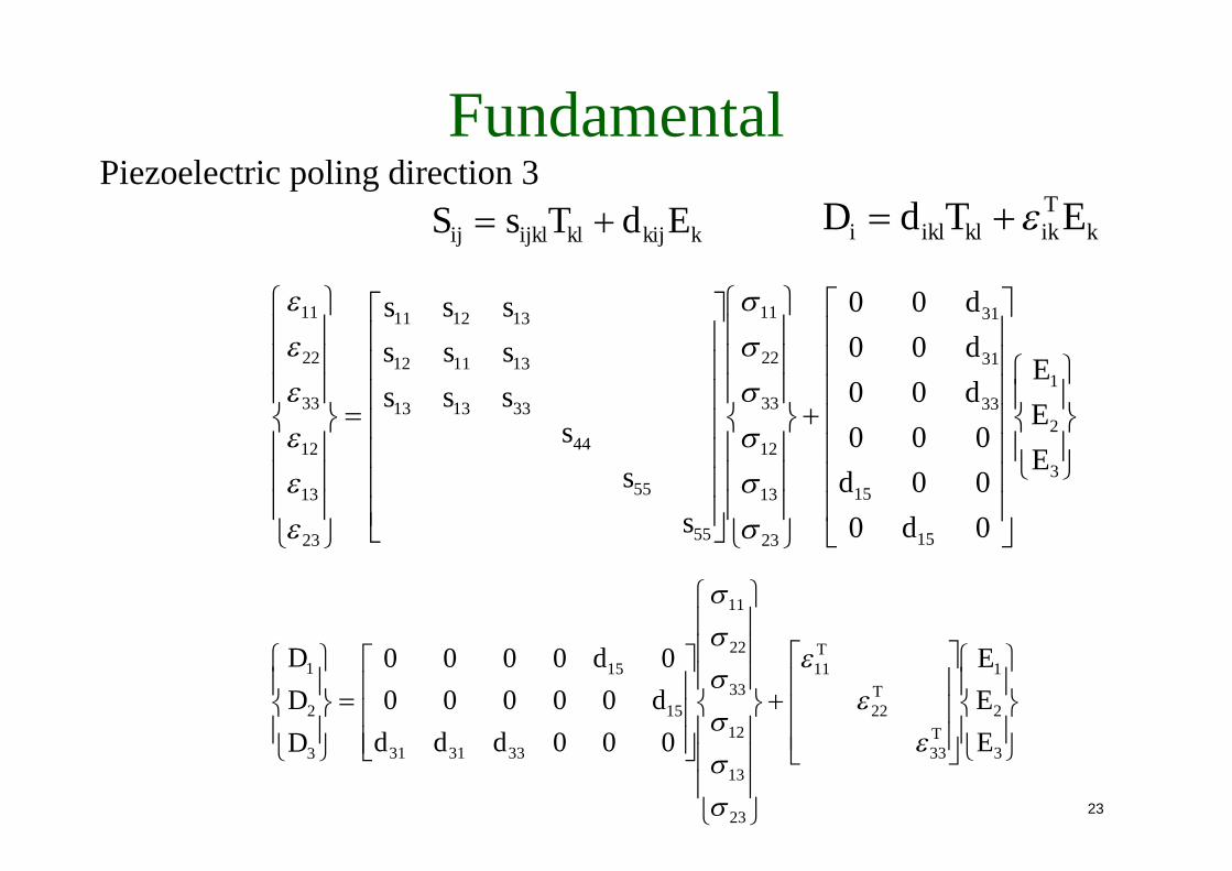
Piezoelectric poling direction 3
23
Fundamental
kkijklijklij EdTsS kTikklikli ETdD
3
2
1
15
15
33
31
31
23
13
12
33
22
11
55
55
44
331313
131112
131211
23
13
12
33
22
11
0000000
000000
EEE
dd
ddd
ss
ssssssssss
3
2
1
33
22
11
23
13
12
33
22
11
333131
15
15
3
2
1
00000000
00000
EEE
dddd
d
DDD
T
T
T
Piezoelectric poling direction 3
24
Piezoelectric harvester•A common material is lead zirconate-titanate,
Pb(Zr,Ti)O3 (PZT).•PMN-PT is a relatively new piezoelectric material.
The advantage of this material is the fourfoldenhancement in the piezoelectric coefficients.However, the two main disadvantages of this materialare the price and the fact that PMN-PT is still in itsinfant stage of development.
25
Piezoelectric harvester•Mode of operation
–d33 mode–d31 mode
26
Vibration energy harvester•Vibration energy to electrical energy•Sources: motors, rotating objects, subways, pipelines,
HVAC systems, bridges, and even the human body
27
Vibrations of the ZigzagMicrostructure for Energy Harvesting•Effective energy harvesting devices typically consist
of a cantilever beam substrate coated with a thin layerof piezoceramic material and fixed with a tip masstuned to resonant at the dominant frequency of theambient vibration.
•The fundamental natural frequency of a beamincreases as its length decreases, so that at the MEMSscale the resonance condition occurs orders ofmagnitude higher than ambient vibration frequencies,rendering the harvester ineffective.
28
A new geometry forMEMS scale cantilever harvesters with
low fundamental frequencies•A “zigzag”geometry would be able to vibrate near
resonance at the MEMS scale.

29
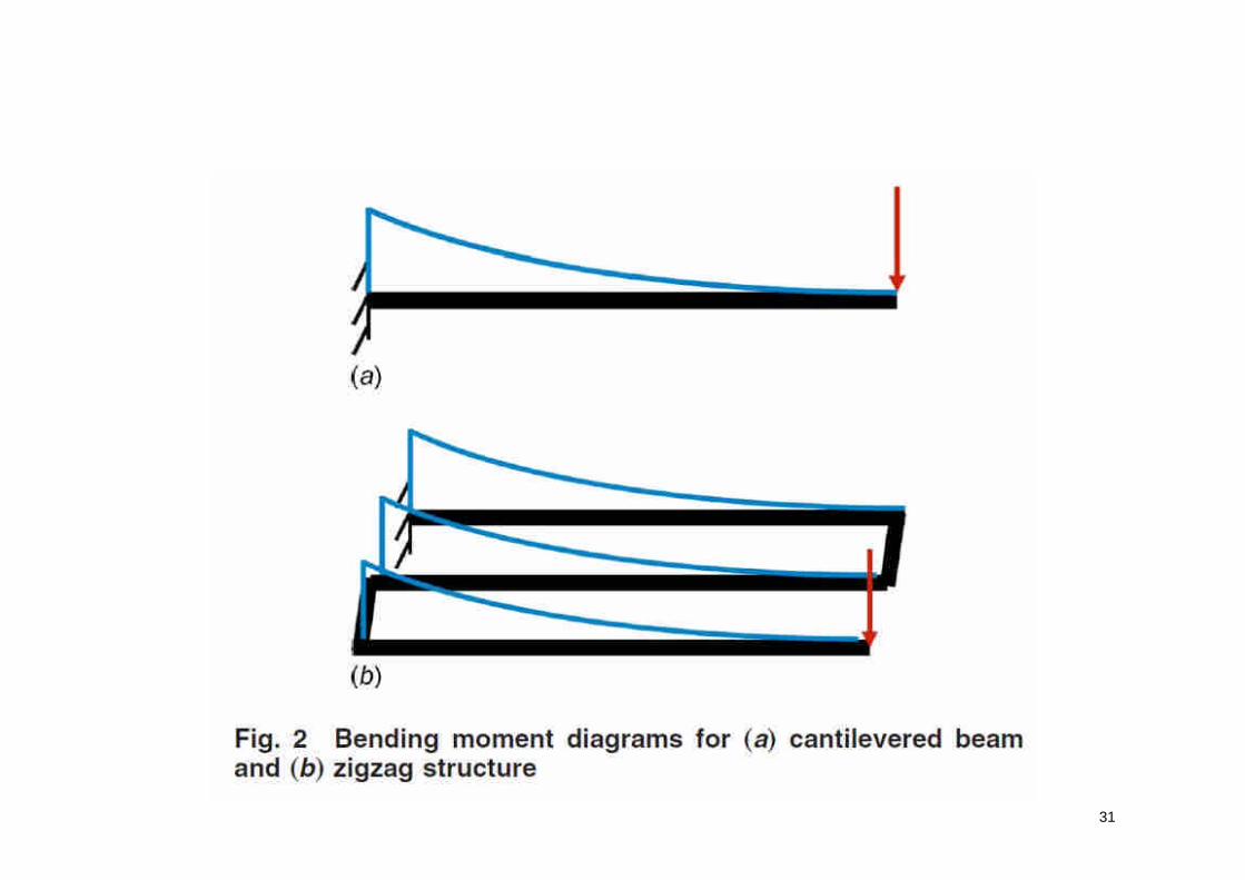
Device structure•Each of the beams can bend out of the main plane and
can twist.
30
•Each of the beams is a uniform composite beamcomposed of a piezoelectric layer bonded to thesubstructure layer (unimorph)
•When the beams are deflected, some strain isgenerated in the piezoelectric layer, which generateselectrical energy.
31
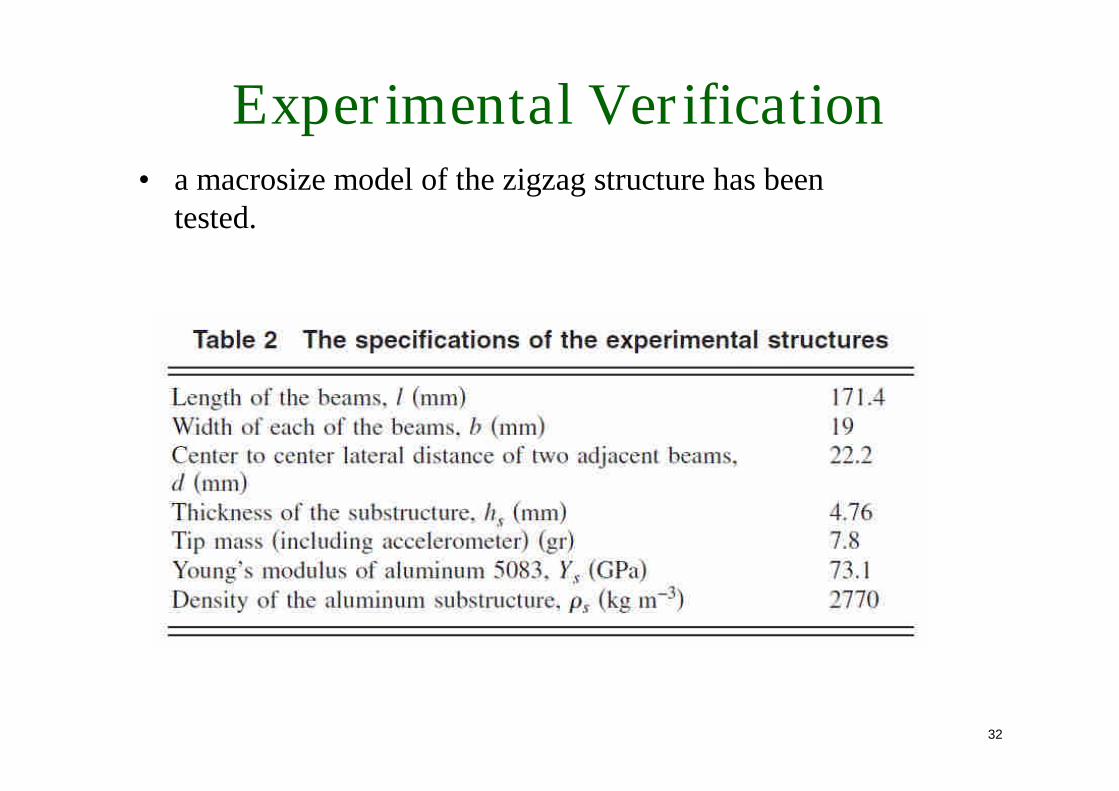
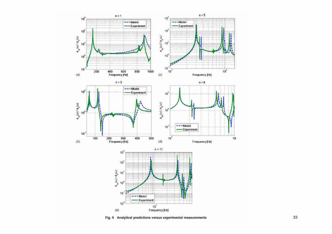
32
Experimental Verification•a macrosize model of the zigzag structure has been
tested.
33
34
Parasitic Power Harvesting in Shoes•Wearable computing—light weight, minimum effort,
high power generation, convenient power delivery,and good power regulation.
•Up to 67 Watts of power are available from heelstrikes during a brisk walk (68 kg person, 2 steps/sec,heel moving 5 cm). (IBM Systems Journal, Vol. 35,No. 3&4, 1996, pp. 618-629)
•Goal to unobtrusively collect energy for low-powerapplications.
35
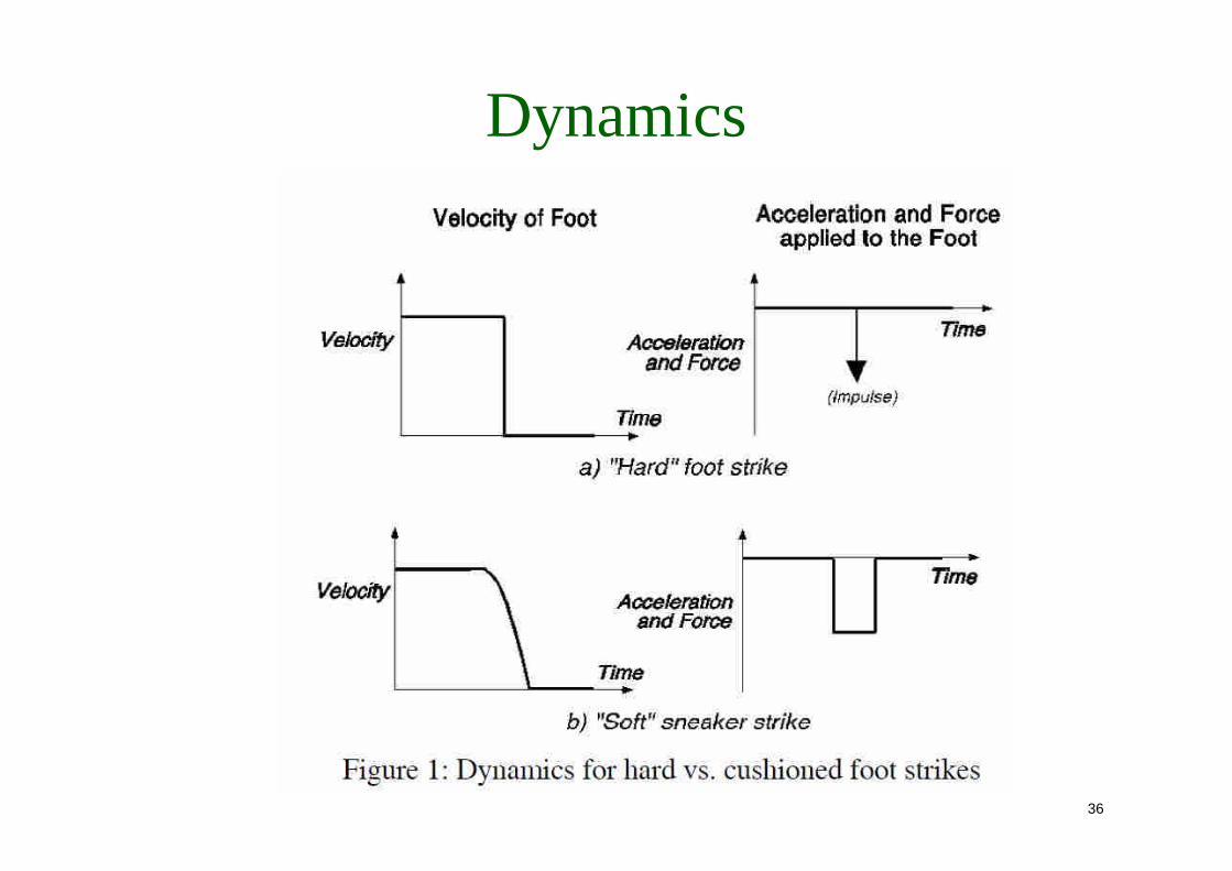
Sport sneaker•Energy dissipating sole.•While walking in ordinary "hard" shoes, the foot is rapidly
decelerated from its relatively high downward speed to zerovelocity relative to the ground—an action that requires theapplication of relatively large and sudden forces to the foot.
•Barring shock absorption in the feet, this can be simplymodeled as a sudden step in velocity; the force applied to thefoot to achieve this deceleration is an impulse
36
Dynamics

37
Dynamics•Function of the insole and midsole in the sport
sneaker is to work as a low-pass filter for this step invelocity, reducing the amount of force applied to thejoints.
•This reduces any stress that the joints experience andalso reduces the incidence of sports injuries.
38
•The result is that the force and displacement values over timefor the bottom and top of the midsole are not the same—as inany passive filter, there is an energy loss in the sole while itperforms this filtering function.
•The energy lost is in the higher harmonics of the step and isdissipated through internal losses in the sole. When the solesprings back after the step it does not exert as much force asbefore, returning less energy than was put into it, and it is thisenergy that we are trying to capture

39
40
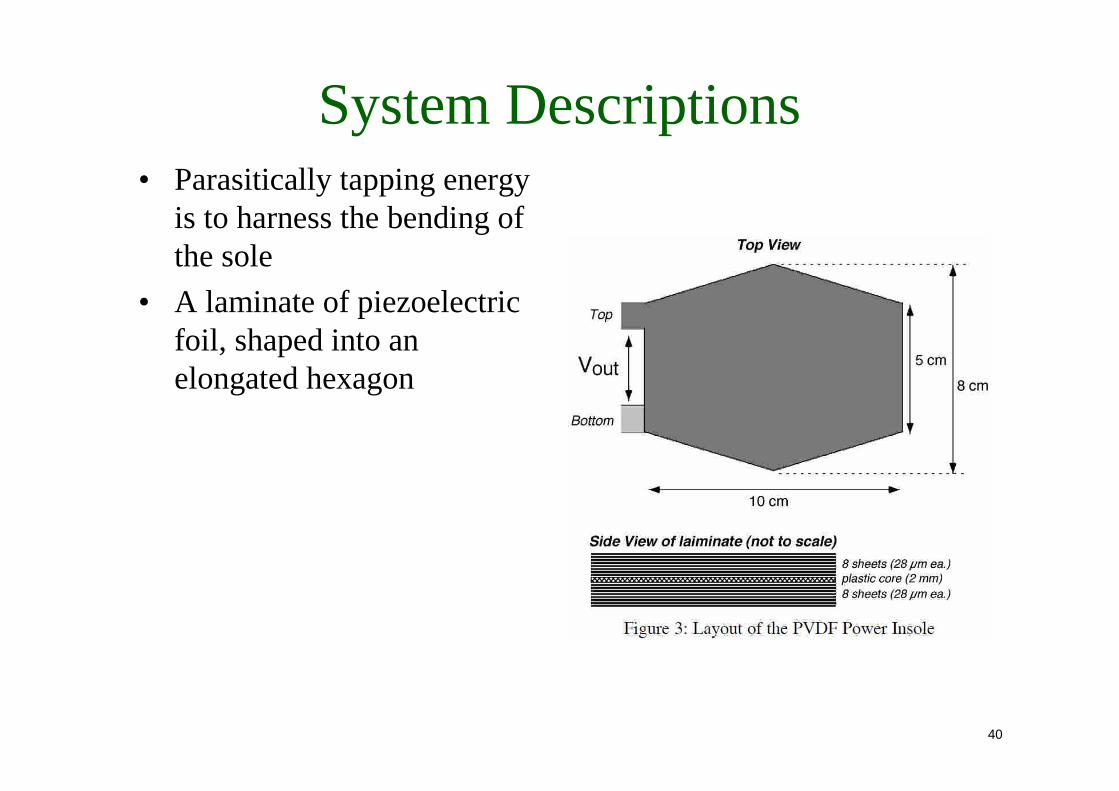
System Descriptions•Parasitically tapping energy
is to harness the bending ofthe sole
•A laminate of piezoelectricfoil, shaped into anelongated hexagon
41
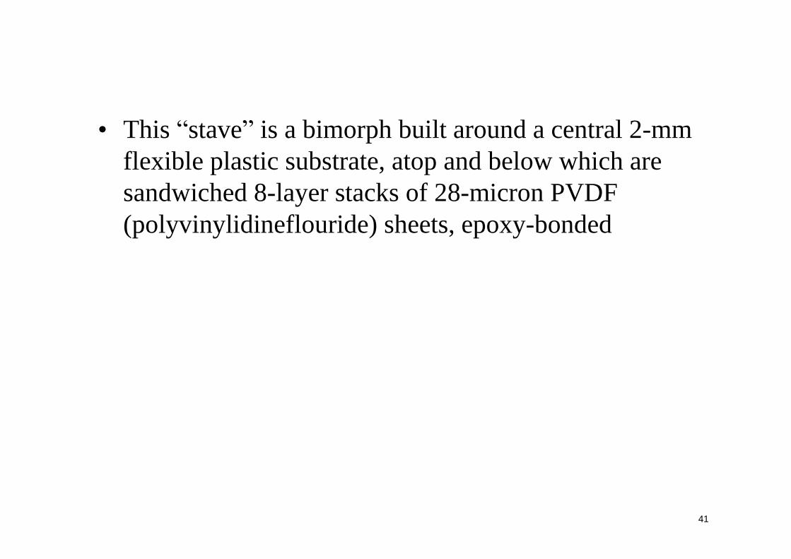
•This “stave”is a bimorph built around a central 2-mmflexible plastic substrate, atop and below which aresandwiched 8-layer stacks of 28-micron PVDF(polyvinylidineflouride) sheets, epoxy-bonded
42
•As the stave is very thin (under 3 mm), it can beeasily molded directly into a shoe sole.
•When the stave is bent, the PVDF sheets on theoutside surface are pulled into expansion, while thoseon the inside surface are pushed into contraction (dueto their differing radii of curvature), producingvoltages across silver-inked electrodes on each sheetthrough the dominant "3-1“longitudinal mode ofpiezoelectric coupling in PVDF.
43
•In order to lower the impedance, the electrodes fromall foil sheets are connected in parallel (switchingpolarities between foils on opposite laminate surfacesto avoid cancellation), resulting in a net capacitanceof 330 nf.
44
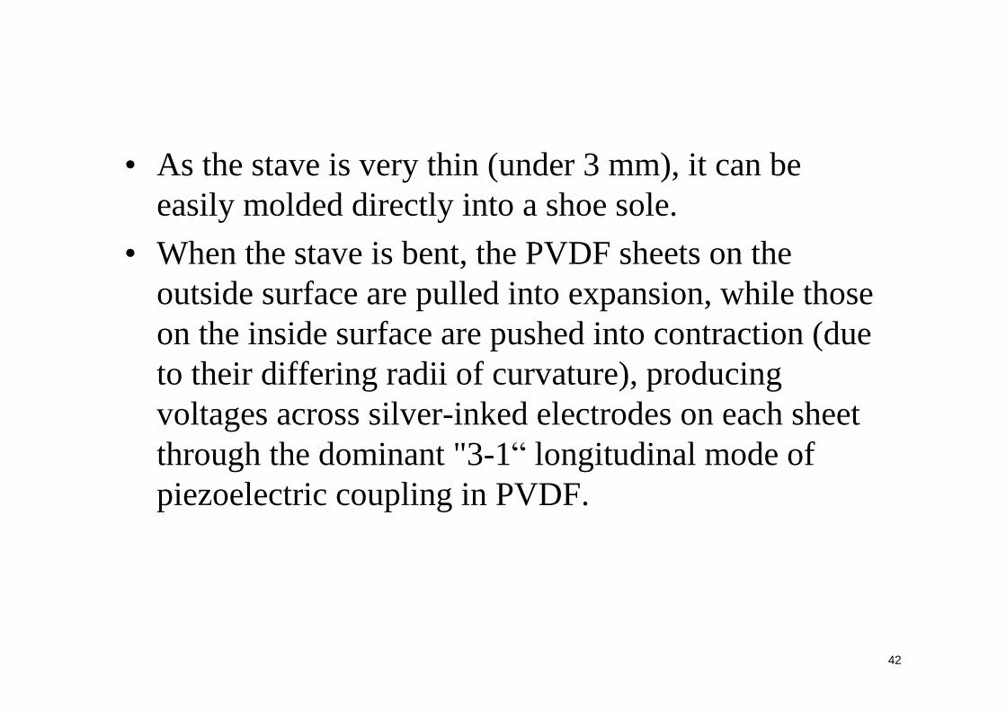
An actual stave
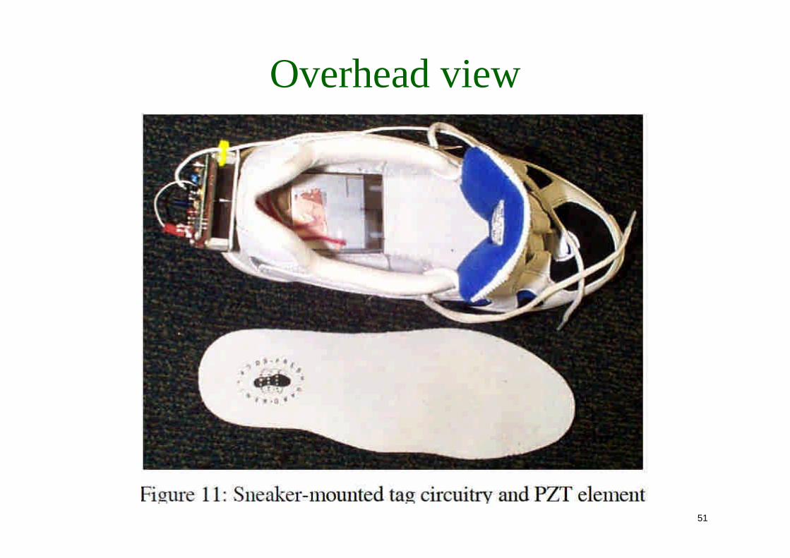
45
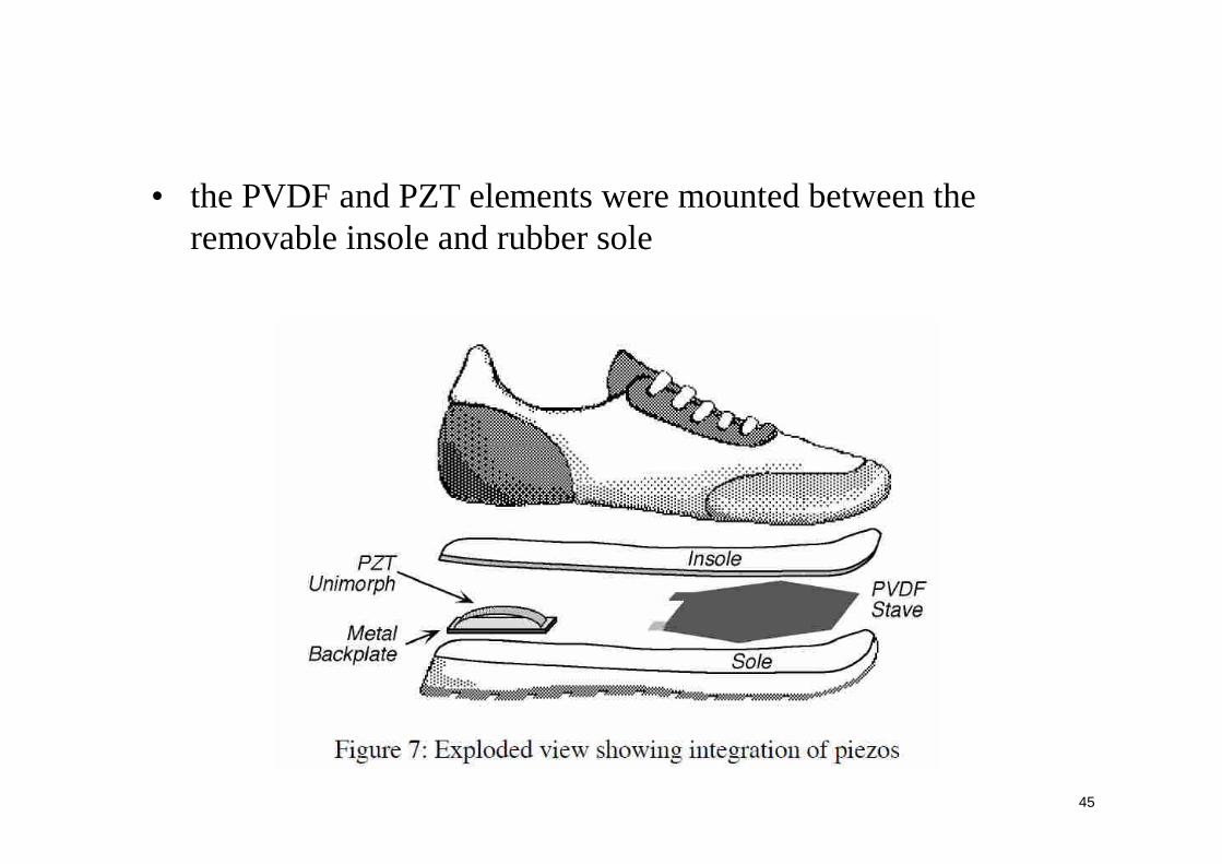
• the PVDF and PZT elements were mounted between theremovable insole and rubber sole
46
•The piezoelectric generators, being high-impedancedevices, were terminated with 250KW resistors,which approximated their equivalent sourceresistance at the excitation frequencies, hence yieldedmaximum power transfer
47
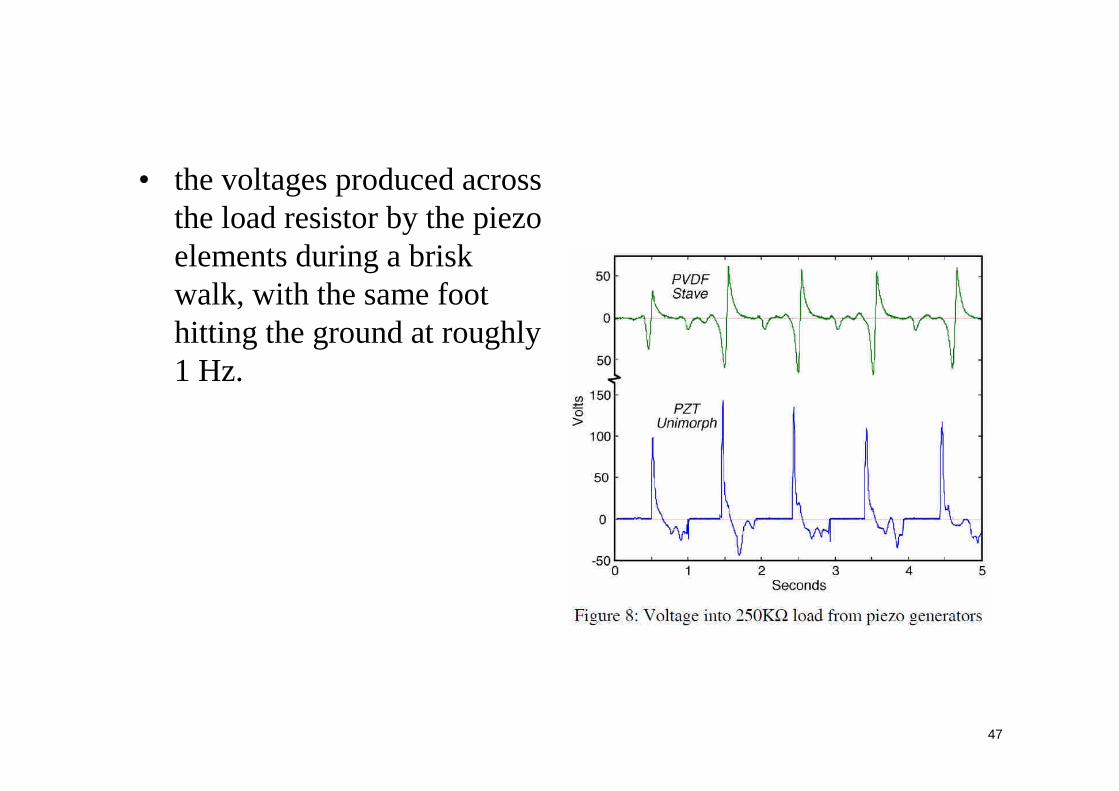
• the voltages produced acrossthe load resistor by the piezoelements during a briskwalk, with the same foothitting the ground at roughly1 Hz.
48
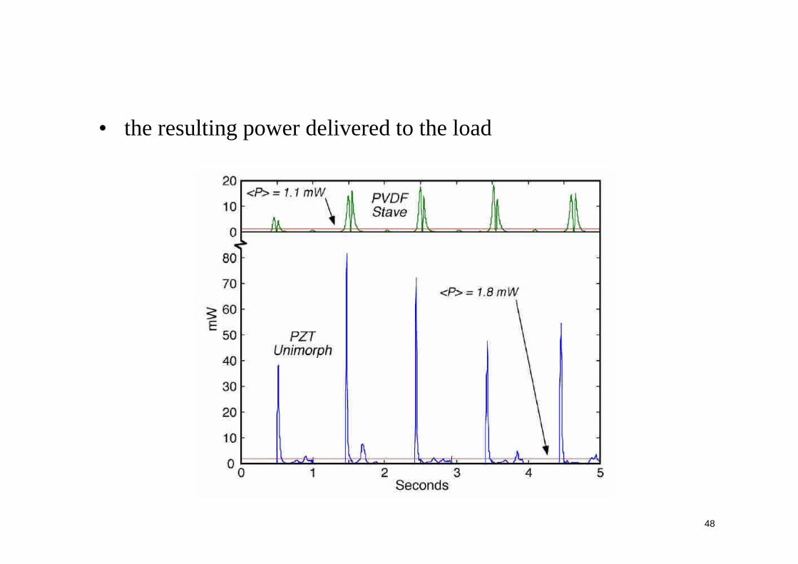
• the resulting power delivered to the load
49
A Self-Powered RF Tag System•A batteryless, active RF tag, which transmits a short-
range wireless ID code to the vicinity while walking.•This has immediate application in active
environments, enabling the user to transmit theiridentity to the local neighborhood while passingthrough and allowing the building to locate itsinhabitants and dynamically channel any relevantresources or information to them.
50
A lowpower RF transmitter•We can mount it in the sneaker and use the energy
extracted from walking to power it without the needfor a battery.
51
Overhead view
52
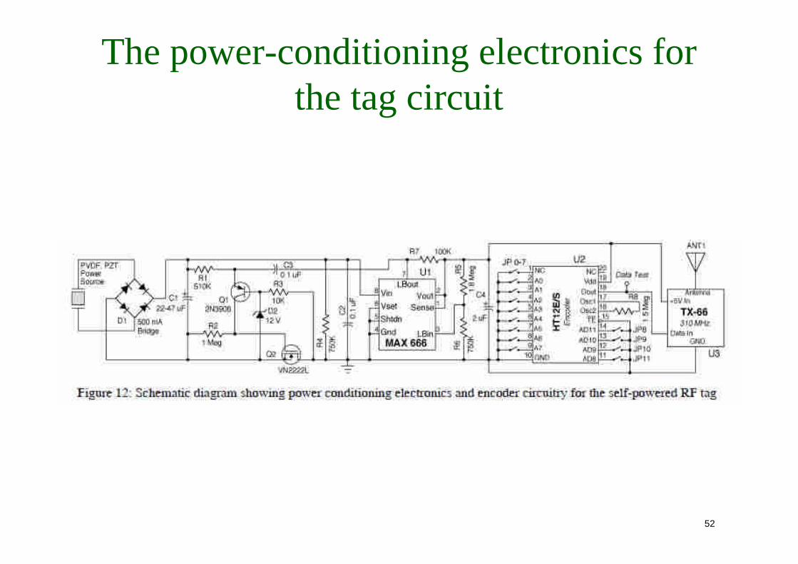
The power-conditioning electronics forthe tag circuit
53
Harvesting circuit•The voltage from the piezo element (e.g., unimorph
or stave) is full-wave rectified in the bridge D1, thencharge is accumulated on the electrolytic capacitor C1.
•The Q1,Q2 circuit acts like an SCR with supercriticalfeedback. It was adapted from a similar circuitdesigned for powering motors off solar cells, revisedto function with the very high impedance of thepiezoelectric sources.
54
A MEMS piezoelectric vibrationenergy harvesters
•Based on AlN and making use of wafer-level vacuumpackaging
•Power a small prototype (1 cm3 volume) of a wirelessautonomous sensor system
•The average power consumption of the whole systemis less than 10 μW, which is continuously providedby the vibration energy harvester.
55
Fabrication•The piezoelectric capacitor is formed by consecutive
deposition, lithography and etching steps of aplatinum bottom electrode, an AlN piezoelectric layerand an aluminum top electrode.
•The silicon mass and beam are shaped by subsequentfront- and backside etching
•Glass-capping wafers with 400 μm deep cavities areetched with hydrofluoric acid and contact holes areobtained with powder blasting.
56
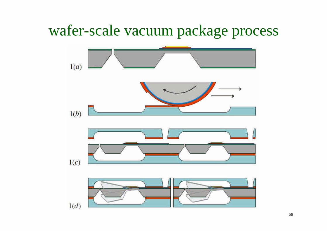
wafer-scale vacuum package process
57
• (a) The AlN piezoelectric capacitor is located on top of thebeam. The Si mass and beam are fabricated by subsequentfront- and backside etching.
• (b) The SU-8 bonding layer is applied with a wafer-scaleroller-coating process on the glass wafers.
• (c) The two glass wafers and the silicon wafer are vacuumbonded in two consecutive bonding steps.
• (d) After dicing, single devices are obtained with the movablemass and beam in the vacuum cavity.
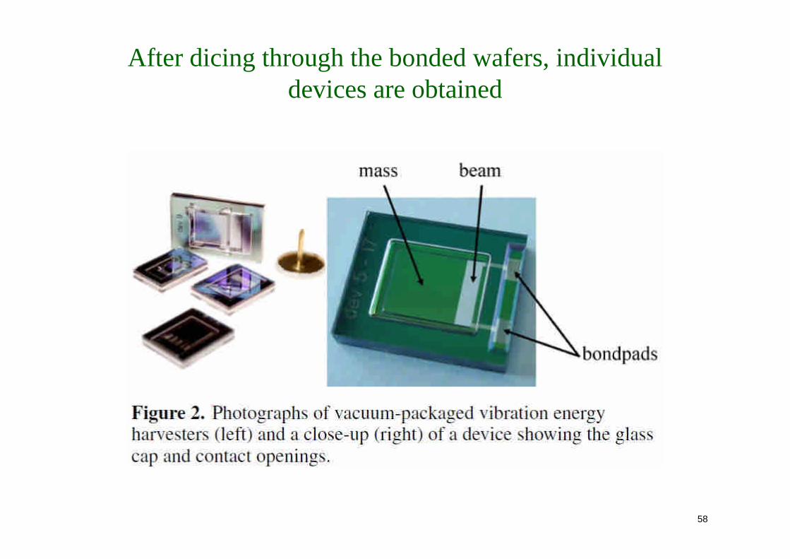
58
After dicing through the bonded wafers, individualdevices are obtained
59
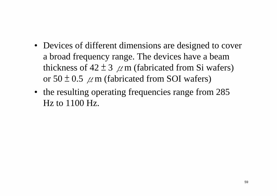
•Devices of different dimensions are designed to covera broad frequency range. The devices have a beamthickness of 42 ± 3 μm (fabricated from Si wafers)or 50 ± 0.5 μm (fabricated from SOI wafers)
•the resulting operating frequencies range from 285Hz to 1100 Hz.
60
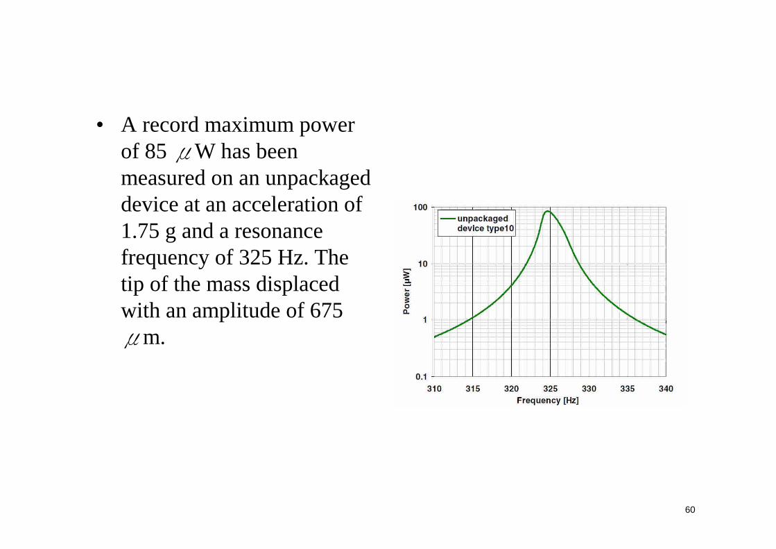
•A record maximum powerof 85 μW has beenmeasured on an unpackageddevice at an acceleration of1.75 g and a resonancefrequency of 325 Hz. Thetip of the mass displacedwith an amplitude of 675μm.
61
Packaging•The package of MEMS harvesters is essential for the
reliability of the fabricated devices as it preventsexcessive mass displacements and protects the siliconbeam from external influences.
•However, the package introduces additional parasitic-damping mechanisms.
62
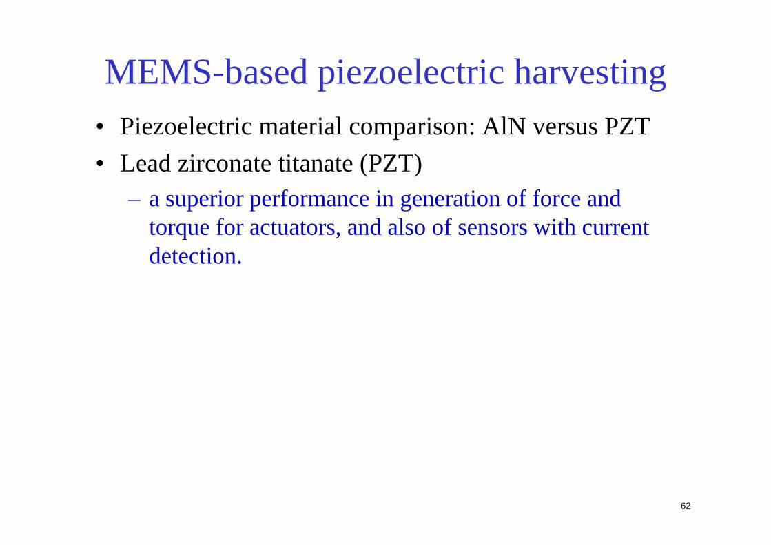
MEMS-based piezoelectric harvesting•Piezoelectric material comparison: AlN versus PZT•Lead zirconate titanate (PZT)
–a superior performance in generation of force andtorque for actuators, and also of sensors with currentdetection.

63
•A higher dielectric constant is generally preferable inenergy harvesting applications as it lowers the sourceimpedance of the device.
•Piezoelectric materials are generally high impedancedevices resulting in the generation of high voltageand low current outputs
64
Dielectric constant•The relative permittivity of a material under given conditions
reflects the extent to which it concentrates electrostatic lines offlux. Technically, it is the ratio of the amount of electricalenergy stored in a material by an applied voltage, relative tothat stored in a vacuum. Similarly, it is also the ratio of thecapacitance of a capacitor using that material as a dielectric,compared to a similar capacitor which has a vacuum as itsdielectric.
•The relative permittivity of a material for a frequency of zerois known as its static relative permittivity or as its dielectricconstant
65
dielectric loss•A loss of energy which eventually produces a rise in
temperature of a dielectric placed in an alternatingelectrical field.
66
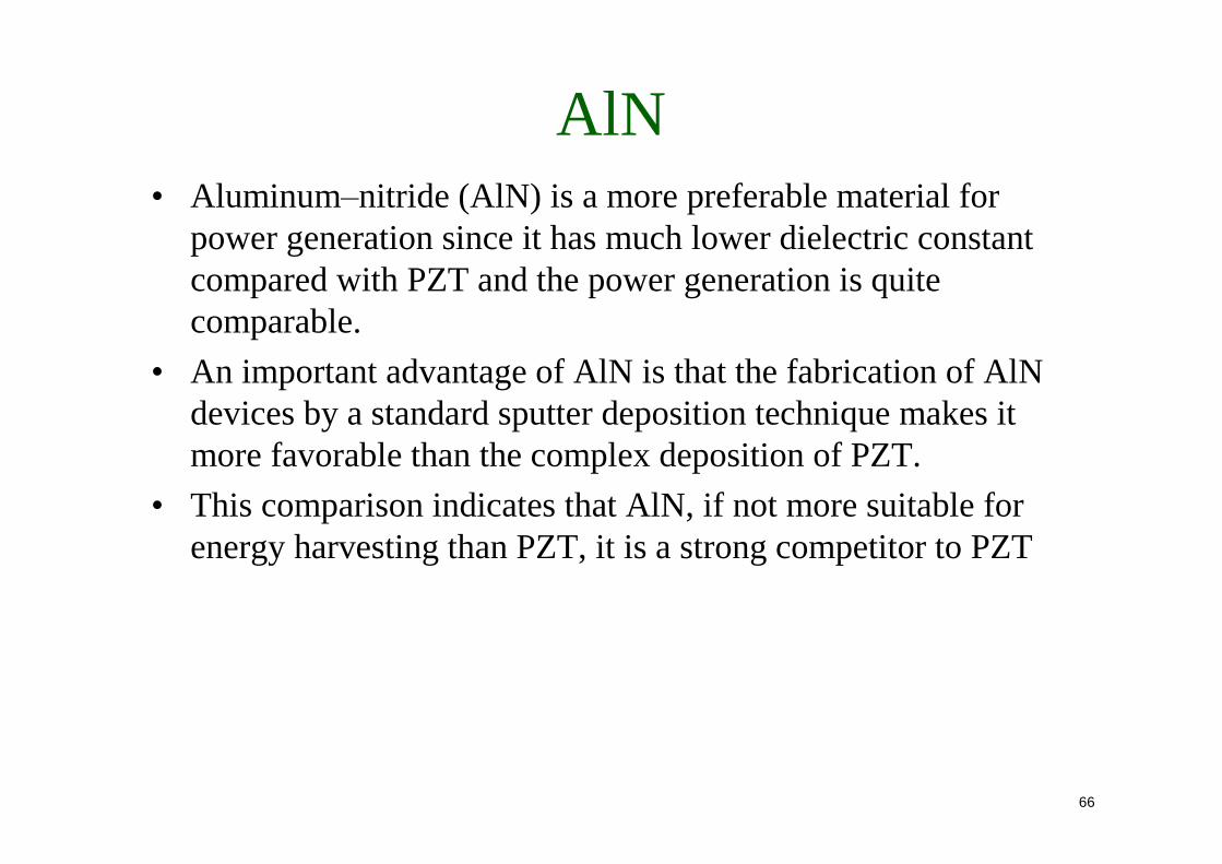
AlN•Aluminum–nitride (AlN) is a more preferable material for
power generation since it has much lower dielectric constantcompared with PZT and the power generation is quitecomparable.
•An important advantage of AlN is that the fabrication of AlNdevices by a standard sputter deposition technique makes itmore favorable than the complex deposition of PZT.
•This comparison indicates that AlN, if not more suitable forenergy harvesting than PZT, it is a strong competitor to PZT

67
Piezoelectric roads for California•California Assemblyman Mike Gatto has proposed a new
bill that will implement piezoelectric technology already inuse in Italy and Israel to harness energy from roadvibrations.

68
Principle•When a car or truck passes over pavement, the
pavement vibrates slightly. By placing relativelyinexpensive piezoelectric sensors underneath a road,the vibrations produced by vehicles can be convertedinto electricity
•Used to power roadside lights, call boxes, andneighbouring communities.
69
•According to one report, "When the technology wasput to the test in 2009, the Israeli government wasable to generate 2,000 watt-hours of electricity simplyby implementing the system on a 10-meter stretch ofhighway."
70
Micro-fabricated piezoelectricvibration energy harvesters
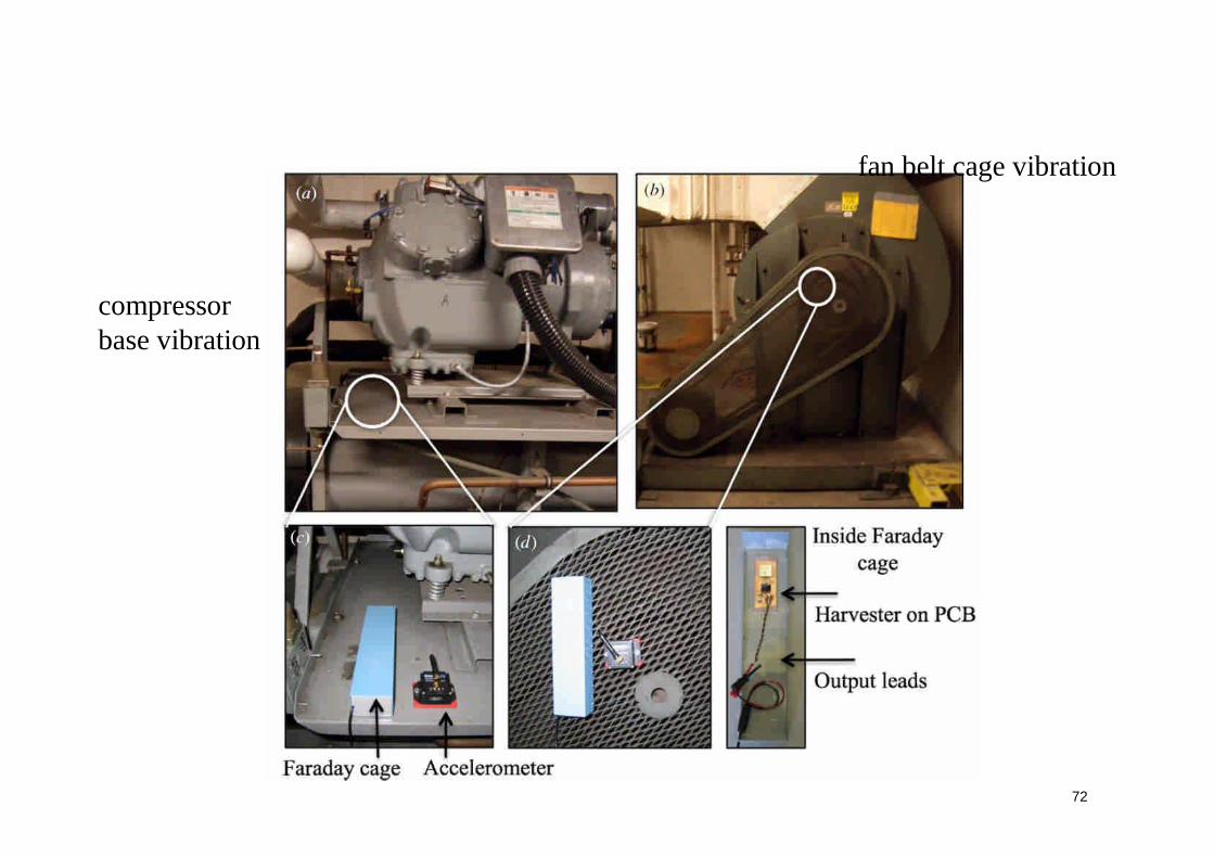
•To harvest energy from ambient vibration sources ina machine room of a large building
•Data were collected at a sampling rate of 2048 Hzusing a Microstrain G-link wireless 3-axisaccelerometer magnetically mounted on the vibrationsource.
•All three axes were surveyed, but in most cases the z-axis (orthogonal to the vibrating surface) accelerationwas an order of magnitude higher than x- and y-axes,so only the z acceleration is used
71
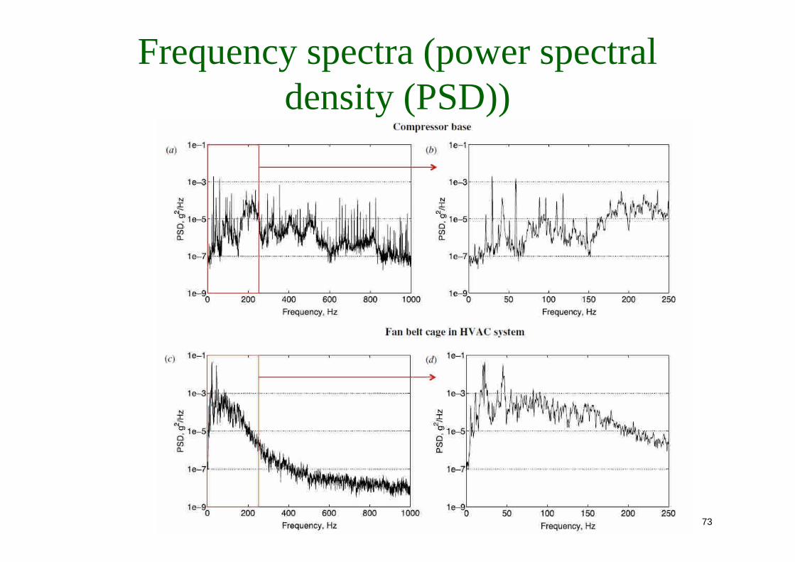
•the dominant frequency peaks from the majority ofthe sources surveyed lie between 20 and 60 Hz, withanother set of frequencies lying between 120 and 140Hz.
•Some sources also contain peaks around 350 Hz.
72
compressorbase vibration
fan belt cage vibration
73
Frequency spectra (power spectraldensity (PSD))
74
PSD in g2/Hz units•Why do we square the sampled data ? This is in order to
obtain a positive quantity. Imagine the signal was a trulyrandom one, containing all frequencies at all amplitudesbetween zero and the peak. This is known as white noise, theanalogy being white light which contains all visiblefrequencies in equal amounts and noise describing no specificpattern of amplitude. If this were the case, then the mean valuewould be zero, because a sampled point would be equally aslikely to have a positive value as a negative value and the netresult after sampling many, many points would be zero.
75
PSD in g2/Hz units•To give us an idea about the variation of the mean-square
value of g² across the frequency range, we progressively filterthe signal from 0Hz to some upper bound that we decide.
•For instance, first we could stop all frequencies above 10Hzand just look at the mean-square value of g² below 10Hz. If wethen divide the mean-square value of g² up to 10Hz by what iscalled the bandwidth of the filter (10Hz in this case) we get thespectral density of the signal in g²/Hz, up to 10Hz. Now wecan increase the filter bandwidth to 20Hz and look at themean-square value now. Again we divide this mean-squarevalue by the filter bandwidth to get the spectral density up to20 Hz. This is repeated this for 30Hz, 40Hz etc..
• If we plot the quantity of mean-square divided by bandwidth(g²/Hz) against frequency (Hz) we get a familiar looking PSDcurve.
76
PSD in g2/Hz units•Actually PSD (Power Spectral Density) is a bit of a
mis-nomer. It should be correcly termed ASD forAcceleration Spectral Density. It has become knownas PSD where the "power" originates from the outputfrom the accelerometers during structural test.
77
Design