drapela GMPES2014 Panel Harmonics · PDF file2 Lighting technologies for general lighting in...
31
Lighting systems Light sources in modern buildings: characterization, modeling and simulations Panel Session: New Harmonic Sources in Modern Buildings 1 Jiri Drapela Brno University of Technology, Czech Republic Roberto Langella Second University of Naples, Iatly IEEE PES General Meeting 2014, July 27-31, Washington DC
Transcript of drapela GMPES2014 Panel Harmonics · PDF file2 Lighting technologies for general lighting in...

Lighting systemsLight sources in modern buildings:
characterization, modeling and simulations
Panel Session: New Harmonic Sources in Modern Buildings
1
Jiri DrapelaBrno University of Technology, Czech Republic
Roberto LangellaSecond University of Naples, Iatly
IEEE PES General Meeting 2014, July 27-31, Washington DC

2
Lighting technologies for general lighting in modern buildings
About 20% of electricity worldwide is consumed by artificial illumination system, thus by light sources (lamps) of different types
Direction according to market studies(residential, public buildings and commercial sectors) High intensity discharge, halogen lighting and incandescent bulbs – in withdrawal Fluorescent lighting – run over and then withdrawal LED lighting – taking market, increasing penetration
Only fluorescent lamps fed by electronic ballasts and LED systems are taken into consideration in the presentation
3
Lighting technologies for general lighting in moder n buildings
Design of converters for lamps vs. Emissions of harmonic currentEmissions are related to circuitry of supply units (ballast and converters/ drivers) which design is subject to following factors: application (replacement of lamps, for designated luminaires, for illumination systems with specific
distribution system, …) qualities (dimming, communication, etc.) requirements of related standards production costs
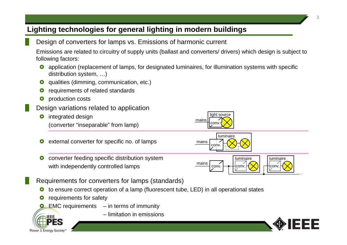
Design variations related to application integrated design
(converter “inseparable” from lamp)
external converter for specific no. of lamps
converter feeding specific distribution system with independently controlled lamps
Requirements for converters for lamps (standards) to ensure correct operation of a lamp (fluorescent tube, LED) in all operational states requirements for safety EMC requirements – in terms of immunity
– limitation in emissions
conv.
light sourcemains
mainsluminaire
conv.
mainsluminaire
conv. conv.
luminaire
conv.

4
Lighting technologies for general lighting in modern buildings
Direct or indirect requirements on /specifications for ballasts and converters design according to the (EU) standards (brief overview)
Lamp – performance and safety specifications
EN 60081 and EN 61195. Double-capped fluorescent lamps.
EN 61167. Metal halide lamps.
…
Lamp controlgear – general (particular), performance and safety requirements
EN 61347-x-y standard series.
EN 60921. Ballasts for tubular fluorescent lamps.
…
Luminaire – general (particular), performance and safety requirements and tests
EN 60598-x-y standard series.
EN 60921. Ballasts for tubular fluorescent lamps.
…..
Luminaire, controlgear – EMC requirements and tests
EN 61547. EMC Immunity requirements. EN 55015. Radio frequency emission limits.
EN 61000-4-y standard series. EN 61000-3-2. Limits for harmonic current emissions
….

5
with capacitive PFC with active PFC
+
-
Y
Y Y
NN
rectifier
HPFNPFLPF
with inductive PFC
+
-
circuit circuitcircuit
N
Y
i
π/2
i
π/2 π/2
i
π/2
i
double stagetopology
Single-Stage (S-S)topology
N
Y Y
EMI Filter
Rectifier Inverter
Driver Ouput stage
230V ~
L
N CB
iv vB
φ
iI
iLvL
Typical circuits of EB for FLs
• screw-basedCFLs (P≤25 W)
• screw-basedCFLs
• screw-based CFLs (small choke –DiscontinuousCurrent Conduction(DCC) - LPF)
• external EB forLFLs (big choke –Continuous CC
• external EB for LFLsand CFLs
• screw-basedCFLs
• external EB forCFLs and LFLs
FL is fed from a Half-bridge resonantvoltage source (or from a Push-Pull) inverter which is supplied from a source ofDC voltage
Electronic Ballast (EB) for Fluorescent Lamps (FLs) - top ologies
6
Drivers (power supplies) for LEDs - topologies
Typical circuits of Drivers/Power supplies for LEDs
L
N
i
v
CD
CB φiL
vL
L
NvB
CB
i
v φiL
vLiI LBK
PWM
φiL
vL
PWM
iI
iIφ
iLvL
Cr
Lr1 Lr2
non-
isol
ated
isol
ated
Voltage divider, used for very low inp. power
There are used the same PFC techniques as in case of EBs.
A map is at at next slide
Buck conv. – “universal input”; Const. Current (CC) or Const. Voltage (CV) output; driver for LP or power LEDs
Flyback conv. – “universal input”; CC or CV output; driver for power LEDsor power supply for LED track, luminaries or lamps
Half-Bridge (HB) resonant conv. –“universal input”; CC or CV output; driver for power LEDs or power supply for LED track, luminaries or lamps
Optimized to supply voltage level;series string of 10-35 mA LEDs (Low-Power LEDs)
7
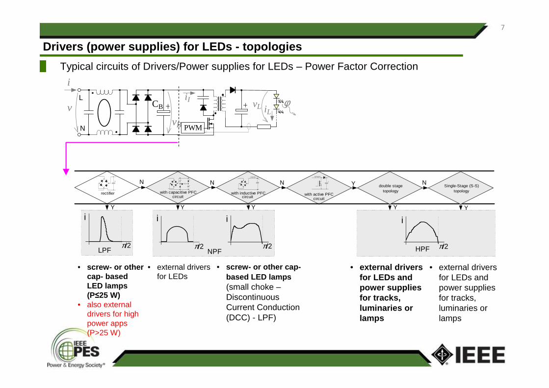
with capacitive PFC with active PFC
+
-
Y
Y Y
NN
rectifier
HPFNPFLPF
with inductive PFC
+
-
circuit circuitcircuit
N
Y
i
π/2
i
π/2 π/2
i
π/2
i
double stagetopology
Single-Stage (S-S)topology
N
Y Y
• screw- or othercap- basedLED lamps(P≤25 W)
• also externaldrivers for highpower apps(P>25 W)
• external driversfor LEDs
• screw- or other cap-based LED lamps(small choke –DiscontinuousCurrent Conduction(DCC) - LPF)
• external driversfor LEDs andpower suppliesfor tracks, luminaries or lamps
• external drivers for LEDs and power supplies for tracks, luminaries or lamps
Drivers (power supplies) for LEDs - topologies
Typical circuits of Drivers/Power supplies for LEDs – Power Factor Correction
L
NvB
CB
i
v φiL
vL
PWM
iI
8
Modeling of lamps with converters
Modeling in time domain Full / switching models – even if simplified/ optimized for specific purposes
Utilization of an accurate model of lamp itself if fed from an electronic converter is not so important for input to input response as the convertor model is. (For Low/Frequency (LF) conducted disturbances study).
Simulations of switching models behaviour are very time consuming….and thus are not suitable for response prediction of large systems or for simulation of long term disturbancesSince information about switching components in input current for mentioned studies is very minor simplifications in modeling can be made
Simplified models linearization linearized modelsaveraging averaged models
Simplified models are created to keep information about LF bandwidth behaviour, i.e. about LF conducted disturbances
Modeling in frequency domain
There are also models and procedures to obtain models for modeling of disturbing loads in frequency domain
Fixed current sources based “equivalent” models Norton “equivalent” models – cross-harmonic complex admittance models
-200
-150
-100
-50
0
50
100
150
200
-0.4 -0.2 0 0.2 0.4Lamp current i L (A)
Lam
p vo
ltage
vL
(V)
for
for
9
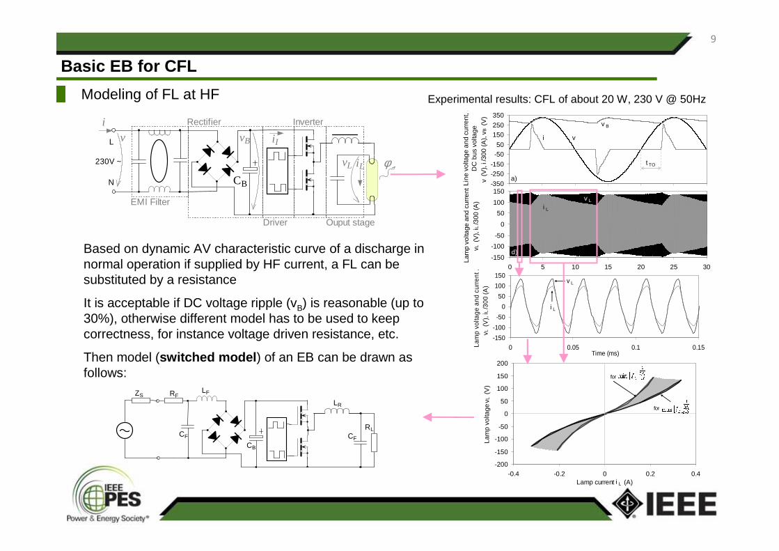
Modeling of FL at HF
ZSLF
CB
CF
RF
LR
CF
RL
-350
-250-150
-5050
150250
350
Line
vol
tage
and
cur
rent
, .
DC
bus
vol
tage
v
(V),
i/30
0 (A
), v B
(V)
v B
i v
t TO
a)
-150
-100
-50
0
50
100
150
0 5 10 15 20 25 30
Time (ms)
Lam
p vo
ltage
and
cur
rent
. v L
(V),
i L/3
00 (A
)
i L
v L
d)
-150
-100
-50
0
50
100
150
0 0.05 0.1 0.15Time (ms)
Lam
p vo
ltage
and
cur
rent
.vL
(V),
iL/3
00 (A
)
v L
i L
Based on dynamic AV characteristic curve of a discharge in normal operation if supplied by HF current, a FL can besubstituted by a resistance
It is acceptable if DC voltage ripple (vB) is reasonable (up to 30%), otherwise different model has to be used to keep correctness, for instance voltage driven resistance, etc.
Then model (switched model ) of an EB can be drawn as follows:
Experimental results: CFL of about 20 W, 230 V @ 50Hz
EMI Filter
Rectifier Inverter
Driver Ouput stage
230V ~
L
N CB
iv vB
φ
iI
iLvL
Basic EB for CFL

10
Frequency
0Hz 125KHz 250KHz 375KHzI(R1)
1.0pA
1.0uA
1.0A
Waveforms of supply voltage (red), input current(green) and of DC bus voltage (blue);Spectra of input current: full and LF part,THDI=146% (up to h=50)
N
R6
430
L4
2.3mH
D3
31
houtL
L2
2mH
1 2+
M2
IRF840
lamp_N
D6R8
10kC6
6.8u
C8
6.8n
lamp_L
V6TD = 0
TF = 0.5uPW = 9uPER = 20u
V1 = 0
TR = 0.5u
V2 = 10
D4
31
houtN
D23
1R1
0.4
R7
.05
R5
.05
C7 33n
D5
31 D7
0
V5TD = 10u
TF = 0.5uPW = 9uPER = 20u
V1 = 0
TR = 0.5u
V2 = 10
R9
10k
M1
IRF840
-
R10
6.8V4
FREQ = 50VAMPL = 325VOFF = 0
Frequency
0Hz 2.0KHz 4.0KHzI(R1)
0A
40mA
80mA
120mA
Time
20ms 30ms 40ms 50ms 60ms1 I(R1) 2 V(L)- V(N) V(+)- V(-)
-400mA
0A
400mA
-700mA
700mA1
>>-400V
-200V
0V
200V
400V2
Simple switched model of a CFL with basic EB
Model in PSpice of a 18W CFL Simulation results
Switching models are only necessary when switching ripples are of interest or detailed transient information is needed
It slows down computing (switching frequency is thousand times higher then system frequency) and information about High Frequency (HF) ripple is useless from point of view of Low-Frequency (LF) disturbances propagation study
Basic EB for CFL
11
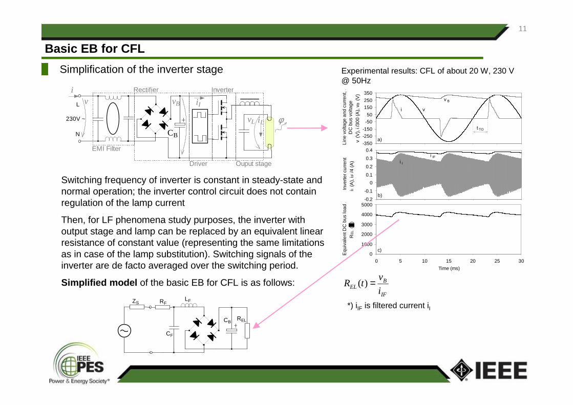
Simplification of the inverter stage
EMI Filter
Rectifier Inverter
Driver Ouput stage
230V ~
L
N CB
iv vB
φ
iI
iLvL
-350
-250-150
-5050
150250
350
Line
vol
tage
and
cur
rent
, .
DC
bus
vol
tage
v
(V),
i/30
0 (A
), v B
(V)
v B
i v
t TO
a)
-0.2
-0.1
0
0.1
0.2
0.3
0.4
Inve
rter c
urre
nti I
(A),
i IF/4
(A) i I
i IF
b)
0
1000
2000
3000
4000
5000
0 5 10 15 20 25 30
Time (ms)
Equ
ival
ent D
C b
us lo
ad .
RE
L (
)
c)
Experimental results: CFL of about 20 W, 230 V @ 50Hz
Switching frequency of inverter is constant in steady-state and normal operation; the inverter control circuit does not contain regulation of the lamp current
Then, for LF phenomena study purposes, the inverter with output stage and lamp can be replaced by an equivalent linear resistance of constant value (representing the same limitations as in case of the lamp substitution). Switching signals of the inverter are de facto averaged over the switching period.
Simplified model of the basic EB for CFL is as follows:
ZSLF
CB
CF
RF
REL
Basic EB for CFL
*) iIF is filtered current iI
IF
BEL i
vtR =)(

12
Time
560ms 570ms 580ms 590ms 600ms1 I(R1) 2 V(L)- V(N) V(+)- V(-)
-500mA
0A
500mA
1
>>-400V
0V
400V2
Frequency
0Hz 2.0KHz 4.0KHzI(R1)
0A
40mA
80mA
120mA
D3
31
D2
31
R10
6.8
N
D5
31
C6
6.8u
0
V4
FREQ = 50VAMPL = 325VOFF = 0
L+
R6
5k
R1
0.4 D4
31
-
L2
2mH
Simplified model of the basic EB for CFL
Model in PSpice of a 18W CFL Simulation results
Waveforms of supply voltage (red), input current(green) and of DC bus voltage (blue);Spectra of input current: THDI=146% (up to h=50)
Simulation results in term of LF part of input current conform with the results obtained for corresponding switching model
Basic EB for CFL

13
Basic EB for CFL performance analysis based on simplified model
Lser
CB
Rser
REL
ELBC RC ⋅=τ
Scheme composed only of essential parts
Magnitude and shape of input / line currrent (i.e.
power and spectral components) are full given by value of Rser, Lser, CB and REL and by their correlation
input power is mainly represented and thus estimated by REL
line current waveform is matter of balance in charging and discharging process over half system period given by CB in relation to REL. An invariant parameter describing the rectifier load there is τC – load/converter time constant:
serial combination of Lser and CB constitutes a series resonant circuit influencing input current by self-oscillations at resonant frequency fr. The
resonant frequency is second invariant parameter of the rectifier.
Expression of fr comes from circuit series impedance:
Thus fr is as follows:
the last one component there is Rser which smooths line current and which can be normalized by CB in form of series time constant or by equivalent capacitive reactance at fundamental frequency:
serBELBserBr
LCRCLCf
⋅⋅=
⋅−
⋅⋅=
ππ 2
111
2
122 &
( ) ( )
⋅⋅⋅⋅+⋅
−⋅+
⋅⋅++=
22
22 1
1
1
ELB
ELB
ser
ELB
ELser
RC
RCLj
RC
RRZ
ωωω
ωω
0.1
1
10
100
1000
10000
10 100 1000 10000f r (Hz)
|Z| (
Ω) L ser = 5H
2H1H
0.5H0.2H
0.1H50mH
20mH10mH
5mH2mH
1mH 0.5mH
C B =10 µF
R EL =5150 Ωτ C =51.5 ms
serBS RC ⋅=τ serBCB
serS RC
X
Rr 1ω==
Basic EB for CFL

14
Basic EB for CFL performance analysis based on simplified model (cont.)
0
50
100
150
200
250
300
350
101001000 τ C (ms)
V B,avg
THD I(I1) (%), h˂40I (mA)
THD I(I) (%), h˂40
∆VB (%)
0
25
50
75
100
101001000 τ C (ms)
(Ih/
I 1).
100
(%)
I 1 /I 1
I 3 /I 1
I 5 /I 1
I 7 /I 1 I 9 /I 1 I 11 /I 1 I 13 /I 1 I 15 /I 1
0
25
50
75
100
1 5 9 13 17 21 25 29 33 37h (-)
(Ih/
I 1).
100
(%)
τ C =10 ms 26 ms
258 ms
103 ms
52 ms
1030 ms 515 ms
Influence of τC
To comply with harmonic current emission limits and to maintain reasonable DC voltage ripple, the τC of CFLs is in range (10)-15-50-(70) ms
The larger τC the shorter conduction time of the rectifier and higher content of harmonics in input current
Simulation results for various τC while Rser=0 Ω, Lser=0 H:
Relative amplitude spectrum of line current for various load/converter time constants
Relative amplitudes of chosen harmonics vs. load/ converter time constant
Chosen circuit quantities vs. load/ converter time constant
Basic EB for CFL

15
Basic EB for CFL performance analysis based on simplified model (cont.)
10
100
1000
10100100010000 f r (Hz)
V B,avg (V)
THD I(I) (%), h<40
THD I(I1) (%), h<40
∆ V B (%)
0
25
50
75
100
10100100010000 f r (Hz)
(Ih/
I 1).
100
(%) I 1
I 3
I 5
I 7
I 9
I 11
I 15
I 13
0
25
50
75
100
1 5 9 13 17 21 25 29 33 37h (-)(I
h/I 1
).10
0 (%
)
fr=712 Hz 503 Hz 356 Hz 225 Hz 113 Hz 36 Hz
16 kHz Hz
2251 Hz 1592 Hz 1125 Hz
Influence of fr
Inductance Lser is composed of three parts representing: a choke in ac or dc part of rectifier “smoothing and improving“current shape, inductance of an EMI filter, if there are employed; and effective inductance of supply network. The frcan be practically in range from 17 kHz to 400 Hz
With decreasing resonance frequency the self-oscillation wave frequency is traveling to lower harmonic order while multi conduction of the input current in each half-period can occur
Simulation results for various fr , for Rser=0 Ω and τC=51.5 ms:
Basic EB for CFL

Frequency
0Hz 0.5KHz 1.0KHz 1.5KHz 2.0KHz 2.5KHz 3.0KHz1 I(R2)
0A
40mA
80mA
120mA1
2
>>
16
Basic EB for CFL performance analysis based on simplified model (cont.)
Analytical solution
τC=51.5 ms , fr=1592 Hz, τS=7.5 µs
Rser=7.5 Ω, Lser=1 mH, CB=10 µF, REL=5150 Ω (blue)Rser=0.75 Ω, Lser=0.1 mH, CB=100 µF, REL=515 Ω (green)
Influence of τS
Summary
Resistance Rser consists of series combination of the supply network effective resistance, used chokes resistances and resistance of a resistor applied in input side of EB to limit inrush current (~ Ohms). The Rser attenuates line current shape and possible resonant oscillations in the current and τS can be practically in range from 0.2 µs to 0.2 ms
The input current waveform is invariant if the rectifier invariant parameters τC, fr and τS are of the same value
En example (simulation results):
Frequency
0Hz 0.5KHz 1.0KHz 1.5KHz 2.0KHz 2.5KHz 3.0KHzI(R2)
0A
0.4A
0.8A
1.2A
Except numerical simulation, the resulting input current waveform can be obtained from solution of analytical description of the simplified model. The most critical part of it there is to find out conduction angles bounding CB capacitor charging and discharging areas, especially in case of multi-conduction
Time
1.480s 1.485s 1.490s 1.495sI(R2)
-10A
0A
10A
Basic EB for CFL
17
EB with passive PFC
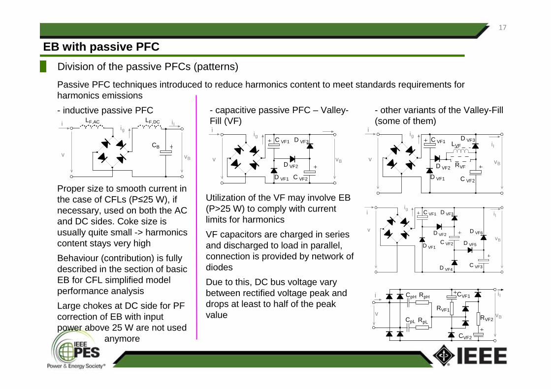
Division of the passive PFCs (patterns)
Passive PFC techniques introduced to reduce harmonics content to meet standards requirements for harmonics emissions
- inductive passive PFC
CB
v
iig
iI
vB
LF,DCLF,AC
C VF2
v
iig
vB
C VF1
D VF1
D VF2
D VF3
- capacitive passive PFC – Valley-Fill (VF)
- other variants of the Valley-Fill (some of them)
C VF2
v
iig
iI
vB
LVFC VF1
D VF1
D VF2
D VF3
RVF
C VF2
v
iig
iI
vB
C VF1
D VF1
D VF2
D VF3
C VF3D VF4
D VF5
D VF6
i
v
iI
vB
CVF1
CVF2
CpL
CpH
RVF2
RVF1
RpH
RpL
Proper size to smooth current in the case of CFLs (P≤25 W), if necessary, used on both the AC and DC sides. Coke size is usually quite small -> harmonics content stays very high
Behaviour (contribution) is fully described in the section of basic EB for CFL simplified model performance analysis
Large chokes at DC side for PF correction of EB with input power above 25 W are not used
anymore
Utilization of the VF may involve EB (P>25 W) to comply with current limits for harmonics
VF capacitors are charged in series and discharged to load in parallel, connection is provided by network of diodes
Due to this, DC bus voltage vary between rectified voltage peak and drops at least to half of the peak value
18
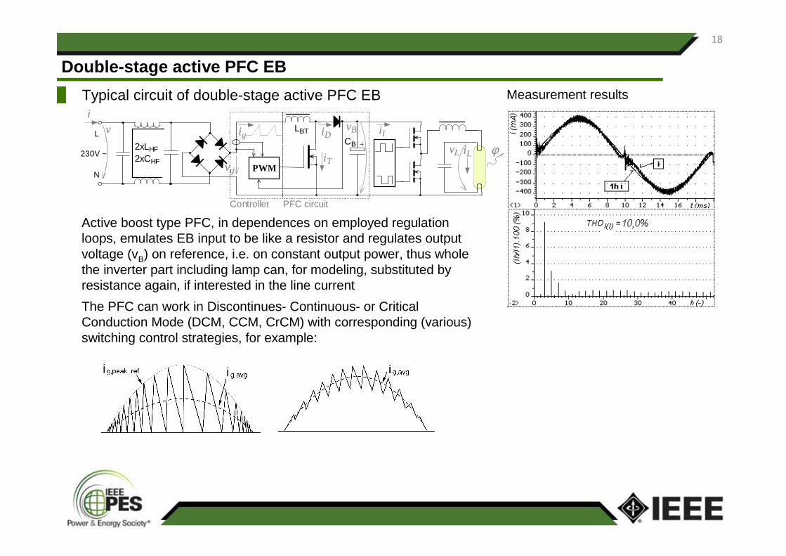
Double-stage active PFC EB
Typical circuit of double-stage active PFC EB
Active boost type PFC, in dependences on employed regulation loops, emulates EB input to be like a resistor and regulates output voltage (vB) on reference, i.e. on constant output power, thus whole the inverter part including lamp can, for modeling, substituted by resistance again, if interested in the line current
The PFC can work in Discontinues- Continuous- or Critical Conduction Mode (DCM, CCM, CrCM) with corresponding (various) switching control strategies, for example:
PWM
CB
LBT
iT
iDig
vg
2xLHF
2xCHF230V ~
L
N
iv
Controller PFC circuit
φiI
iLvL
vB
Measurement results

19
Double-stage active PFC EB
Switching model of an active PFC for EB
D102DN4722
RlowM18k
X1
MTP8N50
cmp
drain
RsL
162m
C1
22n
Rzcd
22k
Rupp1.59Meg
L HV
Rs
13m
RuppM2.2Meg
Cin330nF
Ccmp0.68uF
Rsense2.5
Rlow10k
cs
-
+
MC33262
FB
CMP
MUL
CS ZCD
GND
DRV
VCC
U1 MC33262
R1
0.0001
Dout
MUR130
U2
XFMR10.04692
0 1
2 3
CMUL
10nF
L1
1mH Rstart100k
Resr70m
0
CVcc
100uF
mul
Vinput
FREQ = 50VAMPL = 325VOFF = 0
Rload
4444
D101DN4722
D100DN4722
Lp
1.1mH
Cout40uF
C2
100n
DN4722D103
D1
DN4934
drvL2
1mH
N
Model in PSpice Simulation results
Waveforms of supply voltage (blue), input current(green) and of DC bus voltage (red);Spectra of input current: THDI=5.1 % (up to h=50)
Model represents full controlling with CrCM control strategy, it means switching frequency is changing within period
Again, computing is very time consuming
Content of LF harmonics is very small (THDI practically up to 15%). On other hand PFC causes different time variations in input current when supply voltage magnitude is varying (in depencance on regulation scheme)
0.0
0.5
1.0
1.5
2.0
2.5
3.0
3.5
4.0
4.5
5.0
3 9 15 21 27 33 39h (-)
(IhI
1).1
00 (
%)
.

20
Double-stage active PFC EB
D-S Active PFC EB response to voltage changes
Simulations using switching models are extremely time consuming.
The solution is to apply an averaging technique to obtain an Averaged-switch model
Averaged switch modeling allow us to predict steady-state characteristics and Low-bandwidth dynamics of converters
Measurement results
-400
-200
0
200
400
0 50 100 150 200 250 300Time, t (ms)
Sup
ply
volta
ge, v
(V)
-2
-1
0
1
2
Line
cur
rent
i, I
(A)
v i I(RMS1/2p)
Voltage dip to from 230 to 90 V, duration time of 150 ms

21
Double-stage active PFC EB
Averaged model of the boost rectifier circuit
Signals are averaged over switching period. Average models change the discontinuous system into the continuous system
Substitute for switch-diode combination of the boost DC/DC conv. suitable for both the DCM and CCM with fixed switching frequency fs and variable duty cycle ratio d:
Boost rectifier becomes ideal, assuming that inner wide/bandwidth current controlling loop operates ideally
High-frequency switching components removed by averaging
Line current low-frequency components remain
Resulting model in nonlinear and time-varying
Switch network
+= DCM;
2
CCM;
2
12
2
v
ifLd
dd
u
SBT
+=
2
12
2
2,
vi
fLd
ddMAXu
SBT
CCM/DCM boundary:

22
Frequency
0Hz 0.25KHz 0.50KHz 0.75KHzI(R0)
0A
100mA
200mA
300mA
Time
0.980s 0.985s 0.990s 0.995s1 V(L)- V(N) V(+)- V(-) 2 I(R0)
-500V
0V
500V1
-400mA
0A
400mA2
>>
Time
0.980s 0.985s 0.990s 0.995s1 V(L)- V(N) V(+)- V(-) 2 I(R0)
-500V
0V
500V1
-400mA
0A
400mA2
>>
Frequency
0Hz 0.25KHz 0.50KHz 0.75KHzI(R0)
0A
100mA
200mA
300mA
Double-stage active PFC EB
Averaged model of the boost rectifier circuit (cont.)
Model in PSpice Simulation results
Waveforms of supply voltage (green), input current (blue) andof DC bus voltage (red); Spectra of input current: THDI=27.3 % (up to h=50)
Waveforms of supply voltage (green) distorted by 3rd and 5th
harm. (10%-0°; 5%-180°), input current (blue) and of DC bus voltage (red); Spectra of input current: THDI=17.6 % (up to h=50)
Controlling loop cover Low-bandwidth DC voltage loop only. A part correcting d based on input voltage waveform is not employed. Thus line current distortion is bigger than in case of full voltage loop implementation
The first order PI controller integral time constant is about 20 ms, it means that cut-off frequency of corresponding transfer function is at approx. 8 Hz

23
Time
400ms 450ms 500ms 550ms 600ms 650ms 700ms 750ms 800ms1 V(L)- V(N) V(+)- V(-) 2 I(R0)
-500V
0V
500V1
-1.0A
0A
1.0A2
>>
Time
400ms 450ms 500ms 550ms 600ms 650ms 700ms 750ms 800ms1 V(L)- V(N) V(+)- V(-) 2 I(R0)
-500V
0V
500V1
0A
2.0A
4.0A
6.0A2
>>
Double-stage active PFC EB
Averaged model of the boost rectifier circuit (cont.)
Simulation resultsResponse of the model on slow and rapid supply voltage changes:
a) voltage step from 230 to 115 V (sinusoidal waveform)
b) voltage dip from 230 to 115 V for 100 ms (sinusoidal waveform)
Waveforms of supply voltage (green), input current (blue) andof DC bus voltage (red);
24
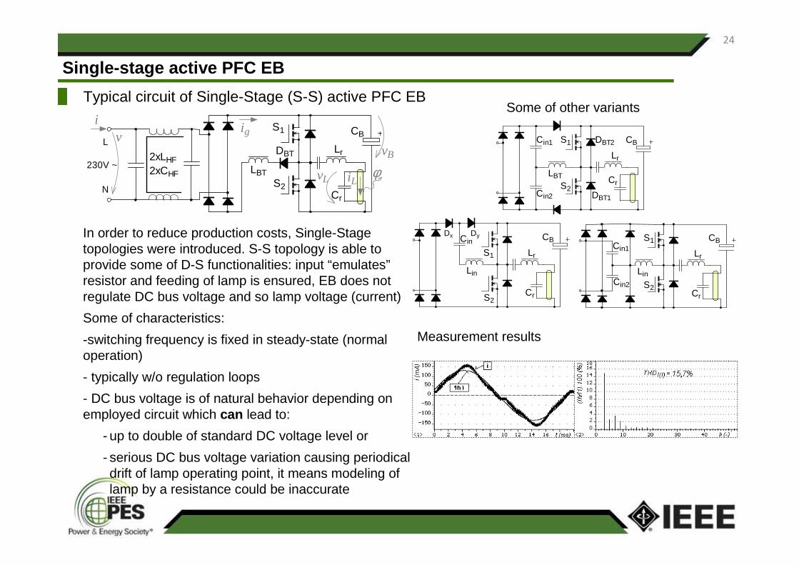
Single-stage active PFC EB
Typical circuit of Single-Stage (S-S) active PFC EB
In order to reduce production costs, Single-Stage topologies were introduced. S-S topology is able to provide some of D-S functionalities: input “emulates”resistor and feeding of lamp is ensured, EB does not regulate DC bus voltage and so lamp voltage (current)
Some of characteristics:
-switching frequency is fixed in steady-state (normal operation)
- typically w/o regulation loops
- DC bus voltage is of natural behavior depending on employed circuit which can lead to:
- up to double of standard DC voltage level or
- serious DC bus voltage variation causing periodical drift of lamp operating point, it means modeling of lamp by a resistance could be inaccurate
Some of other variants
LBT
CB
Lr
Cr
DBT
S1
S2
2xLHF2xCHF
230V ~
L
N
iv
φiLvL
ig
vB
CB
Lr
Cr
Cin
Lin
Dx Dy
S1
S2
CB
Lr
Cr
Cin1
Cin2
Lin
S1
S2
LBT
CB
Lr
Cr
Cin1
Cin2
DBT2
DBT1
S1
S2
Measurement results

25
Single-stage active PFC EB
Switching model of an S-S active PFC for EB
Model in PSpice
M2
IRF840
houtN
D3
31
V5TD = 10u
TF = 0.5uPW = 9uPER = 20u
V1 = 0
TR = 0.5u
V2 = 10
lamp_N
D4
31
N
C4
100n
D7
MUR160
-
R7
.05
R1
0.0001
D2
31
D6
MUR160
R910k
R6
304
C7 33n
L
D8
MUR160
R8
10k
D5
31
+ R5 .05
V4
FREQ = 50VAMPL = 325VOFF = 0
L3
5.0mH
R100.0001
C5
100nlamp_L
L4 3.8mH
houtL
M1
IRF840
C8
6.8n
C6
35u
0
V6TD = 0
TF = 0.5uPW = 9uPER = 20u
V1 = 0
TR = 0.5u
V2 = 10
L2
5mH
1 2
Simulation results
Time
80ms 90ms 100ms 110ms 120ms1 I(R1) 2 V(L)- V(N) V(+)- V(-)
-400mA
0A
400mA1
-0.5KV
0V
0.5KV
1.0KV2
>>
Frequency
0Hz 50KHz 100KHzI(R1)
10uA
1.0A
1.0nA
0.0
2.0
4.0
6.0
8.0
3 7 11 15 19 23h (-)
(IhI
1).1
00 (
%)
.
Waveforms of supply voltage (red), input current(green) and of DC bus voltage (blue);Spectra of input current: THDI=7.9 % (up to h=50)
Model represents S-S interleaved PCF EB
The model can be again simplified using averaging technique if just LF phenomena are subject of interest. Simplification procedure to get averaged-switch model, as in case of D-S active PFC EB can be adopted. In fact the included PFC operate with constant switching frequency and even duty ratio.
26
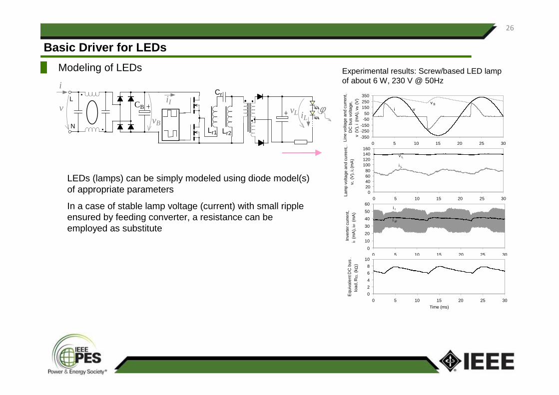
Modeling of LEDs
LEDs (lamps) can be simply modeled using diode model(s) of appropriate parameters
In a case of stable lamp voltage (current) with small ripple ensured by feeding converter, a resistance can be employed as substitute
Experimental results: Screw/based LED lamp of about 6 W, 230 V @ 50Hz
Basic Driver for LEDs
L
NvB
CB
i
viI
φiL
vL
Cr
Lr1 Lr2-350-250-150
-5050
150250350
0 5 10 15 20 25 30Time (ms)
Line
vol
tage
and
cur
rent
, .
DC
bus
vol
tage
, v
(V),
i (m
A),
v B (V
)
vi
v B
020406080
100120140160
0 5 10 15 20 25 30
Time (ms)
Lam
p vo
ltage
and
cur
rent
, .
v L (V
), i L
(mA
)
i L
v L
0
10
20
30
40
50
60
0 5 10 15 20 25 30
Time (ms)
Inve
rter c
urre
nt,
i I (m
A),
i IF (m
A)
i I
i IF
0
2
4
6
8
10
0 5 10 15 20 25 30
Time (ms)
Equ
iva
lent
DC
bu
s .
loa
d, R
EL (k
Ω)

27
Modeling of drivers with LEDsThere is pretty symmetry between LED drivers and EB in modeling:
If the switching converter is of fixed switching frequency and operating with constant duty ratio, whole the second stage of the converter with the LEDs string can be, using averaging method, replaced by an equivalent resistance which loads rectifier as in case of EB. Then following model can be used:
In a case the driver second stage include controlled switching converter, its averaged switch model can be utilized, following already described procedure. The same can be applied for modeling of an active PFC if it is present.
Basic Driver for LEDs
ZSLF
CB
CF
RF
REL
28
References
• ATRA, CH., CONTENTI, C. CFL Ballast with Passive Valley Fill & Crest Factor Control. [on-line]. International Rectifier, Application Note AN-1072, 2004, 7 pp., www.irf.com
• BEN-YAAKOV, S., SHVARTSAS, M., AND GLOZMAN, S. Statics and dynamics of fluorescent lamps operating at high frequency: modeling and simulation [on line]. IEEE Trans. Industry Applications, 38, 6, 1486-1492, 2002 http://www.ee.bgu.ac.il/~pel/pdf-files/jour111.pdf
• BAIRANZADE, M. Electronic Lamp Ballast Design [on line]. Motorola Semiconductor Application Note AN1543/D. https://www.onsemi.com/pub/Collateral/AN1543-D.PDF
• CHANG, G.W., CHEN, S.K., CHEN, G. Harmonic-domain modeling of fluorescent lamp with elec-tromagnetic ballast. Power Engineering Society Summer Meeting, 2001. Vancouver, BC, Canada, IEEE, 2001, Volume: 1, On page(s): 267-270 vol.1, ISBN: 0-7803-7173-9
• CHEN, J., MAKSIMOVIC, D., ERICKSON, R. Buck-Boost PWM Converters Having Two Independ-ently Controlled Switches [on line]. IEEE Power Electronics Specialists Conference, June 2001, 6 pp., http://ece-www.colorado.edu/~pwrelect/Paper_archives/PESC01BB.pdf
• CHUNG, T.J., ET AL. Analysis and design of a single-stage single-switch bi-flyback ac/dc converter. INT. J. ELECTRONICS, VOL. 91, NO. 1, JANUARY 2004, 25–40
• CONTENTI, C., GREEN, P., RIBARICH, T. A new Circuit for Low-Cost Electronic Ballast Passive Valley Fill with additional Control Circuits for Low Total Harmonic Distortion and Low Crest Factor [on line]. International Rectifier, Application Note AN-1074, 2004, 28 pp., www.irf.com
• DRAPELA, J. Backward disturbing influences of light sources on supply distribution system (in Czech). PhD Thesis, Brno University of Technology, 2006, 233 pp.
• DRÁPELA, J.; BOK, J. An improved Valley-Fill passive Power-Factor-Correction circuit for electronic ballast. In Proceedings ot the 9th• International Scientific Conference Electric Power Engineering 2008. 1.Brno, Czech Republic: Brno University of Technology, 2008. s. 149-
155. ISBN:978-80-214-3650- 3.• ERICKSON, R. Fundamentals of Power Electronics [on line]. Chapman and Hall, New York, May 1997, 791 p., http://ece-
www.colorado.edu/~pwrelect/book/slides/slidedir.html , ISBN 0-412-08541-0 • ERICKSON, R., Maksimovic, D. Advances in Averaged Switch Modeling and Simulation [on line]. Power Electronics Specialists Conference,
1999, 169 pp., http://init.knastu.ru/umk/etf/d/Advances_in_Averaged_Switch_Modeling_and_Simulation.pdf• Gole, AM.; Keri, A; Kwankpa, C.; Gunther, E.W.; Dommel, H.W.; Hassan, I; Marti, J.R.; Martinez, J.A; Fehrle, K.G.; Tang, L.; McGranaghan,
M.F.; Nayak, O.B.; Ribeiro, P.F.; Iravani, R.; Lasseter, R., "Guidelines for modeling power electronics in electric power engineering applications," Power Delivery, IEEE Transactions on , vol.12, no.1, pp.505,514, Jan 1997
• GRIGORE, V. Topologycal issues in single-phase power factor correction. Dissertation, Helsinky University of Technology, Finland, 2001.• LAZCANO, M.O., ET AL. Analysis and Design of Power Factor Pre-regulator Based on Symmetrical Charge Pump Circuit Applied to
Electronic Ballast. COBEP 2003, The 7th Brazilian Power Elec-tronics Conf., Fortaleza CE, Brazil, 2003.• LOO, K.H., STONE, D.A., TOZER, R.C., DEVONSHIRE, R. A dynamic conductance model of fluores-cent lamp for electronic ballast design
simulation. IEEE Transactions on Power Electronics, 2005. Volume 20, Issue 5, Sept. 2005, pp. 1178-1185, ISSN 0885-8993• McKinsey&Company. Lighting the way: Perspectives on the global lighting market. Second edition, 2012, 58 pp.• MEDNIK, A. HV9906 SIMPLE TRANSFORMLESS OFF-LINE LED DRIVER FEATURES UNITY POWER FACTOR [on line]. Application note
AN-H47, Supertex, 15.6.2003, 24pp., www.supertex.com

29
References (cont.)
• Middlebrook, R.D., "Small-signal modeling of pulse-width modulated switched-mode power converters," Proceedings of the IEEE , vol.76, no.4, pp.343,354, Apr 1988
• Molina, J.; Sainz, L., "Model of Electronic Ballast Compact Fluorescent Lamps," Power Delivery, IEEE Transactions on , vol.29, no.3, pp.1363,1371, June 2014
• MORICONI, U. Designing a High Power Factor Switching Preregulator with the L4981 Continuous Mode [online]. AN628, STMicroelectronic, 2004, 35pp., www.st.com
• NATIONAL ELECTRICAL MANUFACTURERS ASSOCIATION. Power Quality Implication of Compact Fluorescent Lamps in Residences [on line]. NEMA Lighting System Division Document, Lamp Section, LSD 8-1999, Rosslyn VA USA, April 1999, 18 pp., www.nema.org/products/div2/lsdpowrqual.pdf
• National Semiconductor. 230VAC, 6W- 15W Isolated Flyback LED Driver. Technical Report LM3445, 18 pp.• ON Semiconductor. High Brightness LED Driver Solutions for General Lighting. Report TND345-D, 63 pp., www.onsemi.com• PARTO, P., SMEDLEY, K. Passive PFC for Flyback Convertors [on line]. International Power Con-version and Intelligent Motion Conference
(PCIM 99), Chicago, [cit. 01-08-07], 7 pp., http://www.eng.uci.edu/faculty/smedley/• PEREIRA, E.I., ET AL. Electronic ballast for fluorescent lamps with the PFC stage integrated with the resonant inverter. Power Electronics
Specialists Conference, 2004. PESC 04. 2004 IEEE 35th Annual, Volume 5, 20-25 June 2004 Page(s):4050 – 4056• PHILIPS SEMICONDUCTORS. Electronic ballast controller circuit NE 5565, Product specification 853-1835 16843, May 1996, 6 pp. • PHILIPS. Application guide to fluorescent lamp control gear [on line]. Philips, 2002, 187 pp.,
http://www.dimming.philips.com/download/pdf/fluorescent/applic-guide-fluorescent.pdf• Ribas, J.; Alonso, J.M.; Corominas, E. L.; Cardesin, J.; Rodriguez, F.; Garcia-Garcia, J.; Rico-Secades, M.; Celleja, AJ., "Analysis of lamp-
ballast interaction using the multi-frequency-averaging technique," Power Electronics Specialists Conference, 2001. PESC. 2001 IEEE 32nd Annual , vol.1, no., pp.176,181 vol. 1, 2001
• ŠLEZINGR, J.; DRÁPELA, J.; LANGELLA, R.; TESTA, A. A New Simplified Model of Compact Fluorescent Lamps in the Scenario of Smart Grids. In Proceedings of the 15th IEEE International Conference on Harmonics and Quality of Power (ICHQP 2012). 1. 345 E 47TH ST, NEW YORK, NY 10017 USA: IEEE PES, 2012. pp. 835-841. ISBN: 978-1-4673-1944- 7.
• QIAN, J. Advanced Single-Stage Power Factor Correction Techniques. Dissertation, Virginia Poly-technic Institute and State University, Blacksburg, Virginia, 1997
• QIAO, CH., SMEDLEY, K. A Topology Survey of Single-Stage Power Factor Corrector with a Boost Type Input-Current-Shaper [on line]. University of California (IEEE Applied Power Electronics Conference), Irvine, [cit. 01-08-07], 8 pp., http://www.eng.uci.edu/faculty/smedley/
• RIBARICH, T. IR2159: 250W Metal Halide HID Dimmable Ballast [on line]. Application Note AN-1022, International Rectifier, 233 Kansas Street, El Segundo, CA 90245 USA, 5 pp., www.irf.com
• ROSSETTO, L., SPIAZZI, G., TENTI, P. Boost PFC with 100 Hz Switching Frequency Providing Out-put Voltage Stabilization and Compliance with EMC Standards [on line]. IAS98, 7pp. http://www.dei.unipd.it/~pel/Articoli/

30
References (cont.)
• TAO, F. Advanced High-Frequency Electronic Ballasting Techniques for Gas Discharge Lamps. Dissertation, Center for Power Electronics System, Blacksburg, Virginia, 2001
• Texas Instruments. Using the TPS92070EVM-648 Integrated Dimming LED Lighting Driver Converter for 230 VAC Input. User’s Guide SLUU523, July 2011, 21 pp.
• TURCHI, J. Four Key Steps to Design a Continuous Conduction Mode PFC Stage Using the NCP1653 [on line]. AND8184/D, On Semiconductor, 2004, 8pp., www.onsemi.com
• Z. Wei , N. R. Watson and L. P. Frater "Modelling of compact fluorescent lamps", Proc. 13th IEEE Int. Conf. Harmonics Qual. Power, pp.1 -6, 2008
• Zhu, Huiyu. New Multi-Pulse Diode Rectifier Average Models for AC and DC Power Systems Studies. PhD Thesis, Virginia Polytechnic Institute and State University, 2005, 177 pp. http://scholar.lib.vt.edu/theses/available/etd-12202005-203239/unrestricted/complete_final.pdf
• ANSI C82.77-2002. Harmonic Emission Limits-Related Power Quality Requirements for Lighting Equipment. ANSI Lighting Group – NEMA, 2002
• IEC 61000-3-2 ed.3:2005. Electromagnetic compatibility (EMC) – Part 3-2: Limits – for harmonic current emissions (equipment input current <=16 A per phase)

31
Thank you for your attention
QUESTIONS?