DesignCon 2017 - Ansys...medical applications. The emission of electromagnetic waves from IC chips...
16
DesignCon 2017 Active Power Noise Modeling toward Design for EMI Compliance of IC Chips Akihiko Tsukioka (1) [[email protected]] Naoya Yamamoto (1) [[email protected]] Rie Korenaga (1) [[email protected]] Makoto Nagata (1) [[email protected]] Karthik Srinivasan (2) [[email protected]] Norman Chang (2) [[email protected]] Ying-Shiun Li (2) [[email protected]] Masaya Takahashi (2) [[email protected]] (1) Graduate School of System Informatics, Kobe University, (2) ANSYS Inc.,
Transcript of DesignCon 2017 - Ansys...medical applications. The emission of electromagnetic waves from IC chips...

DesignCon 2017
Active Power Noise Modeling
toward Design for EMI
Compliance of IC Chips
Akihiko Tsukioka(1)
Naoya Yamamoto(1)
Rie Korenaga(1)
Makoto Nagata(1)
Karthik Srinivasan(2)
Norman Chang(2)
Ying-Shiun Li(2)
Masaya Takahashi(2)
(1) Graduate School of System Informatics, Kobe University,(2) ANSYS Inc.,

Abstract
Design of digital IC chips for electromagnetic interference (EMI) is enabled for
electromagnetic compatibility (EMC) conscious applications. Chip-package-system
board (C-P-S) integrated power noise simulation uses passive and active CPMs for an IC
chip with different number of active digital circuits (with different design sizes). The chip
was designed and fabricated in a 65nm CMOS technology, and additionally embedded
on-chip power noise monitors. The power noise waveforms exhibit quantitative
consistency among the C-P-S simulation with a full-chip Si substrate network model and
on-chip power noise measurements with 100 picoseconds and 100 uV resolutions.
Key words: Electromagnetic compatibility, Power integrity, CMOS, Chip power model,
On-chip noise monitor
Author(s) Biography
Akihiro Tsukioka was born in 1992. He graduated from Kobe university in 2015 and
now is a master course student in the graduate school of system informatics, Kobe
university.
Naoya Yamamoto was born in 1993. He graduated from Kobe university in 2015 and
now is a master course student in the graduate school of system informatics, Kobe
university.
Rie Korenaga was born in 1992. She graduated from Kobe university in 2015 and now
is a master course student in the graduate school of system informatics, Kobe university.
Makoto Nagata received the B.S. and M.S. degrees in physics from Gakushuin
University, Tokyo, Japan, in 1991 and 1993, respectively, and the Ph.D in electronics
engineering from Hiroshima University, Japan, in 2001. He was a research associate at
Hiroshima University, Japan, from 1994 to 2002, and then an associate professor of Kobe
University, Japan, from 2002 to 2009. He is currently a professor of the graduate school
of science, technology and innovation, Kobe University.
His research interests include design techniques toward high performance mixed analog,
RF, and digital VLSI systems with particular emphasis on power/signal/substrate
integrity and electromagnetic compatibility, testing and diagnosis, three dimensional
Active Power Noise Modeling toward Design for EMI Compliance of IC Chips

system integration, as well as connectivity and security applications. He was a co-
recipient of the best paper awards from 3D-Test 2013, CHES 2014, and APEMC 2015.
Dr. Nagata has been a member of a variety of technical program committees of
international conferences such as the Symposium on VLSI Circuits (2002-2009), Custom
Integrated Circuits Conference (2007-2009), Asian Solid-State Circuits Conference
(2005-2009), International Solid-State Circuits Conference (2014-), and many others. He
was a technical program chair (2010-2011) and a symposium chair (2012-2013) for
Symposium on VLSI circuits. He is currently an associate editor for IEEE Transactions
on VLSI Systems (2015-). He also served as an associate editor of the IEICE Transactions
on Electronics (2002-2005).
Karthik Srinivasan is currently working as a Senior Corporate AE Manager for Analog &
Mixed Signal Products at Semiconductor Business Unit, Ansys Inc. His work focus includes
providing technical support and guidance to Field Applications Engineers and working
closely with product development teams to plan for future roadmap items. He joined Apache
Design Solutions in 2006 and has taken several roles as part of field AE team. He received a
B.S. in Electronics and Telecommunication Engineering from University of Madras, India,
and an M.S. in Electrical Engineering from the State University of New York, Buffalo in
2003 and 2005 respectively.
Norman Chang co-founded Apache Design Solutions in February 2001 and currently
serves as Chief Technologist at Semiconductor BU, ANSYS, Inc. Prior to Apache, Dr.
Chang lead a group at Palo Alto HP Labs, focused on interconnect related signal/power
integrity issues and contributing to the HP-Intel IA64 micro-processor design. Dr. Chang
received his BS, MS, and Ph.D. in Electrical Engineering and Computer Sciences from
University of California, Berkeley respectively at 1985, 1987, and 1990. He holds twelve
patents and has authored over 50 technical papers. He also co-authored the popular book,
"Interconnect Analysis and Synthesis", published by John Wiley & Sons, 2000. He is
currently in the committee for ESDA-EDA and Si2 Open3D TAB.
Ying-Shiun Li joined Ansys in 2005 and currently serving as Director of Mixed Signal
Product and lead the research and development team to work on transistor-
level power/noise/reliability simulation solutions platform. Prior to joining Ansys, Mr.
Li worked at AmmoCore Technology, a start-up providing a scalable physical
Active Power Noise Modeling toward Design for EMI Compliance of IC Chips

implementation solution for complex SoC designs where he focused on researching and
developing clock and timing optimization algorithms to achieve timing closure of very
large and complex IC designs. Mr. Li holds a Master of Science degree in Electrical
Engineering from University Wisconsin-Madison and a Bachelor of Science degree in
Electrical Engineering from National Taiwan University.
Masaya Takahashi received the bachelor degrees in electronic equipment
communication engineering from Tokyo Denki University, Tokyo Japan, in 1992. He
worked as an Applications Engineer at Mentor Graphics, Celestry design technology,
Cadence design, Apache design solutions from 2006 and he is currently working as an
Area Technical Manager at Semiconductor Business Unit, Ansys Inc.
Active Power Noise Modeling toward Design for EMI Compliance of IC Chips

1. Introduction
Electromagnetic compatibility (EMC) becomes a major concern among IC chips to be
used in electronic sensing and control for critical missions as in vehicle, aviation and
medical applications. The emission of electromagnetic waves from IC chips under active
operation can cause harmful interference to an electronic system, if their strengths exceed
the regulatory levels defined by electromagnetic interference (EMI) standard.
Noise emission from an IC chip is evaluated with the test methods defined in EMI
standards of the series of IEC 61967 [1]. The measurements following to the standards
provide information about the compliance of an IC chip by confirming whether the level
of noise emission in each frequency of interest is below the required threshold. The
requirements are set up in each field of application, according to the regulations or
standards such as [2]. The test methods are typically associated with the power currents
from the IC chip under test (CUT). For example, the one-ohm method captures voltage
waveforms on the one-ohm resistor intentionally inserted in series to a power supply trace
on a printed circuit board (PCB) by an oscilloscope. The magnetic probing method scans
the strength of magnetic field in each frequency with a one-turn coil antenna proximate
to the power supply trace with a spectrum analyzer. Those measurement techniques are
naturally limited to the external environment to the CUT, as is from the objective of EMI
tests. On the other hand, it is strongly desirable for an IC chip designer to grasp the root
cause of power noise generation within an IC chip and improve circuits at the right places
for noise reduction.
In order to make the design process of an IC chip efficient for EMC compliance, this
paper describes generalized simulation techniques of dynamic power supply current of a
digital IC chip. Moreover, a Silicon test vehicle is provided with the on-chip power noise
measurement capability for ensuring the adaptability and accuracy of the techniques.
Once the simulation of dynamic power current is achieved at the IC chip level, the voltage
variations can be estimated on VDD and VSS nodes within circuits and also on VSUB nodes
at various locations on a Si substrate (Fig. 1). This will help designs explore on-chip
countermeasures to reduce noise coupling and interference within and among circuits.
The same power current can be also used for the estimation of EM noise emanated from
the power traces on a PCB as parasitic antenna. This can prompt board designers to place
decoupling capacitors (decaps) or change the design parameters of power management
Active Power Noise Modeling toward Design for EMI Compliance of IC Chips

circuits as remedy against EMI problems.
Figure 1: IC chip power current causes on-chip power noise and on-board EM noise
problems.
The details of EMI simulation methodology will be given in Sect. 2. Then, on-chip noise
monitoring technique will be described in Sect. 3. The design of Silicon test vehicle and
experimental results with comparisons to simulations will be discussed in Sect. 4, and
brief summary will be provided in Sect. 5.
2. Simulation methodology
The IC chip power current problems of (Fig. 1) can be captured in a generalized
equivalent circuit model of the chip-package-system board (CPS) integrated power
delivery network (PDN), as given in Fig. 2. The power traces on a PCB will be modeled
by a full wave solver for the multi-port S parameters and then reduced to lumped RLGC
circuits for the frequency range of interest. The package can be also modeled in S
parameters while often further simplified in the inductance in series (Lwire) since Gold(Au)
bonding wires between IC chip’s pads and package’s lands are dominated by inductance.
The chip internally has dense networks of resistive/inductive and capacitive elements
parasitic to active devices (MOS transistors and associated junction capacitors/diodes)
and passive components (multiple layer metallic wirings.) In the very simplified network
of Fig. 2, the chip model in the PDN is equivalently represented by a single-order RC low
Active
circuits
Impedance
network
Power supply
Board Package IC chipPower current
Power noise
EM noise
Active Power Noise Modeling toward Design for EMI Compliance of IC Chips

pass response for the estimation of power supply line impedance (ZDD). This model is
useful for the exploration of decaps (CDecap) from the frequency response of the entire
PDN.
Figure 2: Chip-package-system board integrated network.
In order to probing power noise problems on an IC chip, the PDN of the chip model needs
to have internal expressions. A chip power model (CPM) of Fig. 3 compactly represents
active power supply current and passive power delivery impedance network of an IC chip.
Chip-package-system(CPS) simulation uses the CPM of the target chip and quantitatively
predicts the voltage variation of power and ground nets within a chip. The size of such
on-chip power noise can be used for relative estimation of electromagnetic (EM) noise
sensed on the board.
While a single CPM can be created for a whole chip, the multiple ones can also represent
respective parts of the chip (blocks) with different nature of circuits. For example, digital
circuits are operating synchronously to a system clock signal and discretely in time. On
the other hand, analog circuits are often continuously processing analog signals and
followed by sampling and digitization for digital processing. These circuits consume
power in very different manners thus should be modeled independently.
A single PDN can be shared among separately captured active prats even in the whole
chip model. Active models for different power domains, for digital circuits with
independent power supplies, or for sensitive analog circuits with power supplies isolated
from the others, are finally merged into a single large PDN with capacitive isolations
(couplings) among them as well as with a single common Si substrate.
RLGC
LWire RDie
CDecap CDie
ZDD
Pkgmodel
PCBmodel
Chipmodel
VDD
VSS
Active Power Noise Modeling toward Design for EMI Compliance of IC Chips
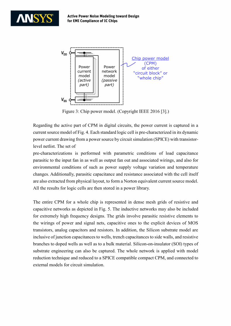
Figure 3: Chip power model. (Copyright IEEE 2016 [3].)
Regarding the active part of CPM in digital circuits, the power current is captured in a
current source model of Fig. 4. Each standard logic cell is pre-characterized in its dynamic
power current drawing from a power source by circuit simulation (SPICE) with transistor-
level netlist. The set of
pre-characterizations is performed with parametric conditions of load capacitance
parasitic to the input fan in as well as output fan out and associated wirings, and also for
environmental conditions of such as power supply voltage variation and temperature
changes. Additionally, parasitic capacitance and resistance associated with the cell itself
are also extracted from physical layout, to form a Norton equivalent current source model.
All the results for logic cells are then stored in a power library.
The entire CPM for a whole chip is represented in dense mesh grids of resistive and
capacitive networks as depicted in Fig. 5. The inductive networks may also be included
for extremely high frequency designs. The grids involve parasitic resistive elements to
the wirings of power and signal nets, capacitive ones to the explicit devices of MOS
transistors, analog capacitors and resistors. In addition, the Silicon substrate model are
inclusive of junction capacitances to wells, trench capacitances to side walls, and resistive
branches to doped wells as well as to a bulk material. Silicon-on-insulator (SOI) types of
substrate engineering can also be captured. The whole network is applied with model
reduction technique and reduced to a SPICE compatible compact CPM, and connected to
external models for circuit simulation.
Chip power model (CPM)
of either “circuit block” or
“whole chip”
Power networkmodel
(passive part)
VDD
VSS
Power currentmodel(activepart)
Active Power Noise Modeling toward Design for EMI Compliance of IC Chips

Figure 4: Pre characterization of digital logic cells for power current source model of
CPM.
(Copyright IEEE 2016 [3].)
Figure 5: A whole chip CPM inclusive of silicon substrate network and connection to
off-chip models. (Copyright IEEE 2016 [3].)
- SPICE simulation: I(t)
LUT for in/out condition, load caps
- Post-layout extraction
logic cell level: Cesc, Resr
Standard cell library (LEF/DEF)
Vss wiring
Vdd wiring
well network
Cesc
I(t) ResrCpg
Cwell
Active Power Noise Modeling toward Design for EMI Compliance of IC Chips

3. Noise measurement methodology
On-chip voltage monitor (OCM) [4][5] captures voltage waveforms on power (VDD),
ground (VSS) and substrate (VSUB) nodes within circuits and at various locations in a
packaged die, as depicted in Fig. 6. The captured waveforms are used for diagnosis of an
system-on-chip die in assembly, regarding such as the frequency domain response of the
PDN, the power and substrate noise coupling between digital and analog/RF circuits, and
the emission of EM noise due to dynamic power current consumption as well as the
susceptibility against incoming EM noises, all associated with power and signal integrity.
Their physical processes are very much complicated and need highly accurate,
reproducible, and appropriately windowed waveform acquisition for in-depth
understanding and reliable characterization. The on-chip measurements also help to
assess the accuracy of power noise simulation.
Figure 6: On-chip monitoring function mounted on an IC chip.
The system diagram of OCM is given in Fig. 7. The probing front end (PFE) circuitry
provides input channels, senses and digitizes input voltage, VIN, seen at the wiring of
interest. The channel consists of a source follower and a latch comparator. The voltage
CMOS circuits
On-chip voltagemonitor (OCM)
Printed circuit board (PCB)
VSSVDDVSUB
PackageIC chip
Power noise
Active Power Noise Modeling toward Design for EMI Compliance of IC Chips

(VIN) continuously sensed by a source follower (SF) is DC offset at its output (VSFO) and
strobed at the timing (TSTRB) defined by a timing clock generator (TG), and approximated
to the nearest reference voltage (VREF) produced by a reference voltage generator (VG).
The nearest search across the space of VREF voltage is performed in response to the output
of a latch comparator (DOUT), assuming iterative operations of a target circuit to diagnose.
Finally, the nearest VREF voltage to VSFO as the replica of VIN (with offset voltage) is
determined at the timing of TSTRB. This process is repeatedly continued with the next
timing point of TSTRB+ T, and the resultant set of sampled points {VREF(TSTRB)} provides
the on-chip digitized voltage waveform of VIN. The OCM captures reference sinusoidal
waveforms with known amplitude in the calibration phase to cancel the offset voltage of
SF and also to compensate the voltage gain.
The PFE channels are prepared for a variety of voltage domains of interest, from the
highest voltage of I/O power supply to a common ground voltage. The offset voltage of
a source follower is intentionally tailored for each voltage domain of interest so as to
maintain a constant input DC voltage given to the following comparator. An external
micro controller communicates with internal operating blocks of the OCM as well as the
external TG and VG through data communication bus and executes the search algorithm
as the function of output probability of a latch comparator. The output streams from the
comparator are measured by a data processing unit (DPU) and accumulated in an output
register. Then, the waveform capturing is fully automated and embedded in the
measurement system of the target chip.
Figure 7: On-chip voltage monitoring system mounted on an IC chip.
PFE PFEData Proc.
UnitPFEPFE
Reference voltage (VREF) Timing clock (TSTRB)
Data Out
VIN TSTRB
VREF
VSFO
VREF > VSFO → DOUT = ‘1’
VSFO > VREF → DOUT = ‘0’
DOUT
SF LC
Active Power Noise Modeling toward Design for EMI Compliance of IC Chips

The OCM was demonstrated in a 65nm CMOS prototype, as shown in Fig. 8, with the
spurious-free dynamic range (SFDR) of 63.2 dB for 400 mV sinusoid at 1 MHz, if with
the resolutions of 800 uV for VREF and 640 psec. for T of TSTRB. An effective bandwidth
is also measured as 700 MHz. The configurable resolutions and selectable DC voltage
offsets allow the OCM for the wide coverage of voltage domains from VDD to VSS.
Figure 8: Accuracy of on-chip voltage waveform acquisition.
4. EMI simulation with Silicon test vehicle
A test chip of Fig. 9 uses a 65nm CMOS technology and includes several digital cores
that can be selectively activated for different levels of activity. The chip also embeds
probing channels of the OCM in an array, to measure time-domain voltage variation as
power noise on a various point of PDN shared by the digital cores. The chip area is 4 mm
x 3 mm and mounted directly on the PCB with a chip-on-board assembly technique.
While this eliminates the package substrate, bonding wires remain for direct connection
between I/O pads of the chip to metallic bonding lands patterned on the PCB.
SFDR63.2 dB
-140
-120
-100
-80
-60
-40
-20
0
105
106
107
108
Frequency(Hz)
Am
plitu
de(d
BV
)
Vin-pp:800 mVResolution 800 μV / step640 ps / step
Frequency(Hz)
Gai
n(dB
)
-18
-16
-14
-12
-10
-8
-4
-2
0
1 10 100 1000
700 MHz
Resolution 200 μV / step10 - 640 ps / step
Active Power Noise Modeling toward Design for EMI Compliance of IC Chips

Figure 9: Silicon test vehicle in 65nm CMOS technology.
Power noise waveforms have been simulated in the C-P-S simulation environment with
CPMs derived for the test chip in multiple operation scenarios with different number of
active digital cores (also with different design sizes). The C-P-S simulation additionally
incudes a full-chip Si substrate model as the part of power delivery network (PDN), where
the digital circuits with CMOS logic cells have resistive connections to the p-type Si
substrate through p+ substrate contacts. The derived CPM and equivalent PCB and
package models are simulated with SPICE simulator.
The on-chip power noise measurements have also been performed with the test chip
operating accordingly to each scenario, finely in time and voltage resolutions of 100
picoseconds and 100 uV, respectively. The whole measurement system is built for the
OCM and digital cores to operate synchronously to each other.
The simulated and measured power noise waveforms on the power (VDD) and ground
(VSS) nodes are compared in Fig. 10. The waveforms exhibit sharp drops due to peak
power consumption current and are followed by over or under shoots due to the resonance
of parasitic inductance, capacitance and resistance to the PDN. The overall shape of the
waveforms, and more importantly, the size of peak drops as the function of the number
of active digital circuits are well consistent among the simulation and measurements. The
larger peak drop is due to the higher amount of dynamic power consumption current, and
results in the stronger electromagnetic emission (EMI) from the power trace of printed
circuit board.
P1
P2
P3
Interface
P4
D C B A
On-
chip
mon
itor
Active Power Noise Modeling toward Design for EMI Compliance of IC Chips

Figure 10: On-chip measured and C-P-S simulated waveforms on power and ground
nodes.
The magnitude of noise is defined as V0P, as shown in Fig. 11. The highest drop, either
negative or positive for VDD and VSS, respectively, are measured from the nominal DC
voltage and averaged for consecutive clock cycles.
Figure 11: Definition of noise amplitudes.
The trends of the magnitude of noise are evaluated as the function of the number of
digital cores in operation. Regarding power noise (Fig. 12), the size of negative drop
Sim
. w/ C
PM
VDD VSS
Mea
s. b
y O
CM
The average for 4 cycles (drops) as V0P
Power VDD
Ground VSS
V0P
V0P 1080
1090
1100
1110
1120
1130
1140
1150
1160
1170
1180
0 100 200 300 400 500 600 700 800 900 1000 1100 1200 1300
Vol
tage
[mV
]
time[ns]
V0P
Active Power Noise Modeling toward Design for EMI Compliance of IC Chips

increases with the number of active cores. The slopes among simulation with CPMs and
measurements by OCM are consistent, exhibiting the proper modeling of dynamic
power supply current and static passive impedance of PDN.
Figure 12: Comparison of power noise magnitudes on VDD with different number of
active cores.
In addition, the trends of substrate noise amplitude are given in Fig. 13. The size of V0P
measured on the p-type substrate is almost 1/5 of that on power node internally in digital
circuits. This is naturally understood that the current propagating through the Si substrate
is sufficiently smaller than the ground current primarily flowing through VSS wiring, and
further attenuated by the distance from the digital circuits in operation to the substrate tap
probed by the OCM. The trend is correlated between measurements and simulation.
Figure 13: Comparison of substrate noise magnitudes on VSUB with different number of
active cores.
-0.06
-0.05
-0.04
-0.03
-0.02
-0.01
0
1 2 3 4
V0p
(V)
# of active cores
RH-NA
RH-CAP
TT-CSM
TT-CSM-CAP
MEAS
-0.06
-0.05
-0.04
-0.03
-0.02
-0.01
0
1 2 3 4
V0p
(V)
# of active cores
TT-CSM MEAS
1.20 V
Simulation (CPM)
On-chip measurements(OCM)
Simulated Measured
0.000
0.005
0.010
0.015
0.020
0.025
0.030
1 2 3 4
V0p
(V)
# of active cores
TT-CSM (Psub) MEAS
0.0 V
Digital circuits OCM
Probed point on Si substrate Simulated Measured
Active Power Noise Modeling toward Design for EMI Compliance of IC Chips

5. Conclusions
The CPS integrated PDN model with passive and active parts of CPM are demonstrated
to be effective for full-chip level power noise simulation, with multiple digital cores with
different operating contents. The Silicon substrate model is also included for precisely
capturing power current flows on metal wirings as well as in a semiconductor material to
I/O pads in connection to the power trace and plains on the PCB. Simulation results on a
65 nm CMOS test vehicle quantitatively explain measured dynamic power and substrate
noise with the OCM. The CPS integrated simulation technique with CPM enables the
design of digital IC chips for EMI compliance in EMC conscious applications.
References
[1] IEC 61967-6: Integrated circuits - Measurement of electromagnetic emissions, 150 kHz to 1 GHz
- Part 6: Measurement of conducted emissions - Magnetic probe method.
[2] LIN EMC Test Specification, Rev. 2.2, Dec. 2010, http://www.lin-subbus.org.
[3] M. Nagata, “T8: Noise Simulation in Mixed-Signal SoCs,” in IEEE Intl. Solid-State Circuits
Conference, Tutorial, Feb. 2016.
[4] K. Noguchi, M. Nagata, "An On-Chip Multi-Channel Waveform Monitor for Diagnosis of
Systems-on-Chip Integration," IEEE Trans. VLSI Systems, vol.15, no. 10, pp. 1101-1110, Oct.
2007.
[5] T. Hashida, M. Nagata, “An On-Chip Waveform Capturer and Application to Diagnosis of Power
Delivery in SoC Integration,” IEEE J. Solid-State Circuits, vol. 46, no. 4, pp. 789-796, Apr. 2011.
Active Power Noise Modeling toward Design for EMI Compliance of IC Chips