
DATASHEET SEARCH SITE == · FLASH and EEPROM block protect Development Support Single-wire...
357
深圳市南天星电子科技有限公司 专业代理飞思卡尔 (Freescale) 深圳市南天星电子科技有限公司 电话:0755-83040796 传真:0755-83040790 邮箱:[email protected] 网址:www.soustar.com.cn 地址:深圳市福田区福明路雷圳大厦 2306 室 飞思卡尔主要产品 8 位微控制器 16 位微控制器 数字信号处理器与控制器 i.MX 应用处理器 基于 ARM®技术的 Kinetis MCU 32/64 位微控制器与处理器 模拟与电源管理器件 射频器件(LDMOS,收发器) 传感器(压力,加速度,磁场, 触摸,电池) 飞思卡尔产品主要应用 汽车电子 数据连接 消费电子 工业控制 医疗保健 电机控制 网络 智能能源
Transcript of DATASHEET SEARCH SITE == · FLASH and EEPROM block protect Development Support Single-wire...

深圳市南天星电子科技有限公司 专业代理飞思卡尔
(Freescale) 深圳市南天星电子科技有限公司 电话:0755-83040796 传真:0755-83040790 邮箱:[email protected] 网址:www.soustar.com.cn 地址:深圳市福田区福明路雷圳大厦 2306室
飞思卡尔主要产品
8位微控制器 16位微控制器 数字信号处理器与控制器 i.MX应用处理器 基于 ARM®技术的 Kinetis MCU 32/64位微控制器与处理器 模拟与电源管理器件 射频器件(LDMOS,收发器) 传感器(压力,加速度,磁场,触摸,电池)
飞思卡尔产品主要应用
汽车电子
数据连接 消费电子 工业控制 医疗保健 电机控制 网络 智能能源
HCS08Microcontrollers
freescale.com
MC9S08EL32MC9S08EL16MC9S08SL16MC9S08SL8Data Sheet
MC9S08EL32Rev. 37/2008

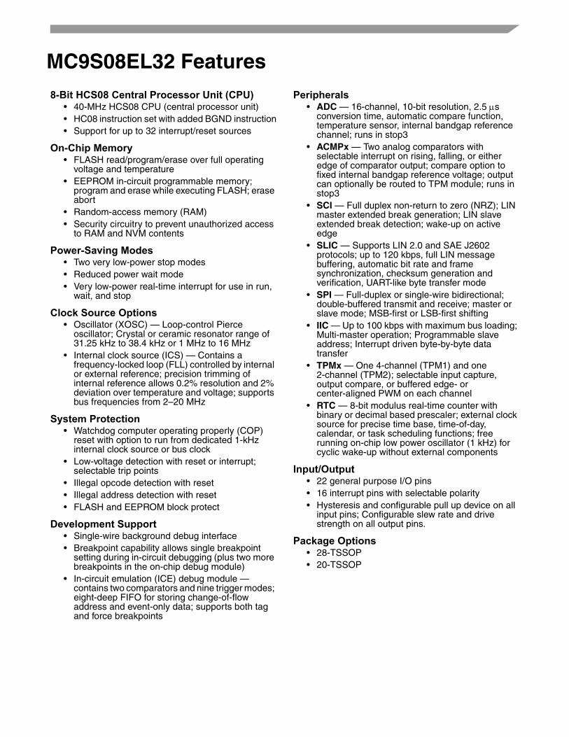
8-Bit HCS08 Central Processor Unit (CPU)• 40-MHz HCS08 CPU (central processor unit)• HC08 instruction set with added BGND instruction• Support for up to 32 interrupt/reset sources
On-Chip Memory• FLASH read/program/erase over full operating
voltage and temperature• EEPROM in-circuit programmable memory;
program and erase while executing FLASH; erase abort
• Random-access memory (RAM)• Security circuitry to prevent unauthorized access
to RAM and NVM contents
Power-Saving Modes• Two very low-power stop modes• Reduced power wait mode• Very low-power real-time interrupt for use in run,
wait, and stop
Clock Source Options • Oscillator (XOSC) — Loop-control Pierce
oscillator; Crystal or ceramic resonator range of 31.25 kHz to 38.4 kHz or 1 MHz to 16 MHz
• Internal clock source (ICS) — Contains a frequency-locked loop (FLL) controlled by internal or external reference; precision trimming of internal reference allows 0.2% resolution and 2% deviation over temperature and voltage; supports bus frequencies from 2–20 MHz
System Protection• Watchdog computer operating properly (COP)
reset with option to run from dedicated 1-kHz internal clock source or bus clock
• Low-voltage detection with reset or interrupt; selectable trip points
• Illegal opcode detection with reset• Illegal address detection with reset • FLASH and EEPROM block protect
Development Support• Single-wire background debug interface• Breakpoint capability allows single breakpoint
setting during in-circuit debugging (plus two more breakpoints in the on-chip debug module)
• In-circuit emulation (ICE) debug module — contains two comparators and nine trigger modes; eight-deep FIFO for storing change-of-flow address and event-only data; supports both tag and force breakpoints
Peripherals• ADC — 16-channel, 10-bit resolution, 2.5 μs
conversion time, automatic compare function, temperature sensor, internal bandgap reference channel; runs in stop3
• ACMPx — Two analog comparators with selectable interrupt on rising, falling, or either edge of comparator output; compare option to fixed internal bandgap reference voltage; output can optionally be routed to TPM module; runs in stop3
• SCI — Full duplex non-return to zero (NRZ); LIN master extended break generation; LIN slave extended break detection; wake-up on active edge
• SLIC — Supports LIN 2.0 and SAE J2602 protocols; up to 120 kbps, full LIN message buffering, automatic bit rate and frame synchronization, checksum generation and verification, UART-like byte transfer mode
• SPI — Full-duplex or single-wire bidirectional; double-buffered transmit and receive; master or slave mode; MSB-first or LSB-first shifting
• IIC — Up to 100 kbps with maximum bus loading; Multi-master operation; Programmable slave address; Interrupt driven byte-by-byte data transfer
• TPMx — One 4-channel (TPM1) and one 2-channel (TPM2); selectable input capture, output compare, or buffered edge- or center-aligned PWM on each channel
• RTC — 8-bit modulus real-time counter with binary or decimal based prescaler; external clock source for precise time base, time-of-day, calendar, or task scheduling functions; free running on-chip low power oscillator (1 kHz) for cyclic wake-up without external components
Input/Output• 22 general purpose I/O pins• 16 interrupt pins with selectable polarity• Hysteresis and configurable pull up device on all
input pins; Configurable slew rate and drive strength on all output pins.
Package Options• 28-TSSOP• 20-TSSOP
MC9S08EL32 Features

MC9S08EL32 Data SheetCovers MC9S08EL32
MC9S08EL16MC9S08SL16MC9S08SL8
MC9S08EL32Rev. 37/2008
Freescale™ and the Freescale logo are trademarks of Freescale Semiconductor, Inc.
© Freescale Semiconductor, Inc., 2008. All rights reserved.
MC9S08EL32 Series and MC9S08SL16 Series Data Sheet, Rev. 3
6 Freescale Semiconductor
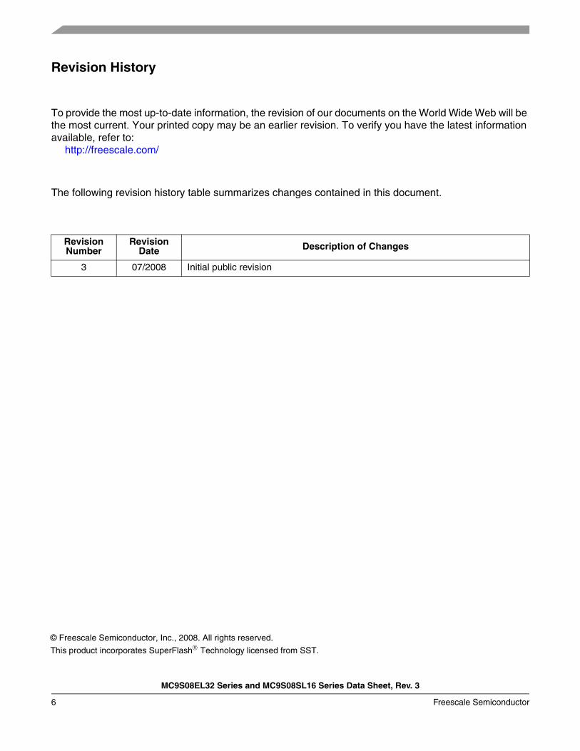
Revision History
To provide the most up-to-date information, the revision of our documents on the World Wide Web will be the most current. Your printed copy may be an earlier revision. To verify you have the latest information available, refer to:
http://freescale.com/
The following revision history table summarizes changes contained in this document.
RevisionNumber
RevisionDate Description of Changes
3 07/2008 Initial public revision
© Freescale Semiconductor, Inc., 2008. All rights reserved.
This product incorporates SuperFlash® Technology licensed from SST.
MC9S08EL32 Series and MC9S08SL16 Series Data Sheet, Rev. 3
Freescale Semiconductor 7
List of Chapters
Chapter 1 Device Overview ...................................................................... 19
Chapter 2 Pins and Connections............................................................. 25
Chapter 3 Modes of Operation................................................................. 31
Chapter 4 Memory..................................................................................... 37
Chapter 5 Resets, Interrupts, and General System Control.................. 63
Chapter 6 Parallel Input/Output Control.................................................. 79
Chapter 7 Central Processor Unit (S08CPUV3) ...................................... 95
Chapter 8 Internal Clock Source (S08ICSV2)........................................ 115
Chapter 9 5-V Analog Comparator (S08ACMPV2)................................ 129
Chapter 10 Analog-to-Digital Converter (S08ADCV1)............................ 137
Chapter 11 Inter-Integrated Circuit (S08IICV2) ....................................... 165
Chapter 12 Slave LIN Interface Controller (S08SLICV1) ........................ 185
Chapter 13 Serial Peripheral Interface (S08SPIV3) ................................ 233
Chapter 14 Serial Communications Interface (S08SCIV4)..................... 249
Chapter 15 Real-Time Counter (S08RTCV1) ........................................... 269
Chapter 16 Timer Pulse-Width Modulator (S08TPMV2) ......................... 279
Chapter 17 Development Support ........................................................... 307
Appendix A Electrical Characteristics...................................................... 331
Appendix B Ordering Information and Mechanical Drawings................ 355

MC9S08EL32 Series and MC9S08SL16 Series Data Sheet, Rev. 3
8 Freescale Semiconductor
MC9S08EL32 Series and MC9S08SL16 Series Data Sheet, Rev. 3
Freescale Semiconductor 9
Contents
Section Number Title Page
Chapter 1Device Overview
1.1 Devices in the MC9S08EL32 Series and MC9S08SL16 Series .....................................................191.2 MCU Block Diagram ......................................................................................................................201.3 System Clock Distribution ..............................................................................................................23
Chapter 2Pins and Connections
2.1 Device Pin Assignment ...................................................................................................................252.2 Recommended System Connections ...............................................................................................26
2.2.1 Power ................................................................................................................................262.2.2 Oscillator ...........................................................................................................................272.2.3 RESET ..............................................................................................................................272.2.4 Background / Mode Select (BKGD/MS) ..........................................................................282.2.5 General-Purpose I/O and Peripheral Ports ........................................................................28
Chapter 3Modes of Operation
3.1 Introduction .....................................................................................................................................313.2 Features ...........................................................................................................................................313.3 Run Mode ........................................................................................................................................313.4 Active Background Mode ...............................................................................................................313.5 Wait Mode .......................................................................................................................................323.6 Stop Modes ......................................................................................................................................32
3.6.1 Stop3 Mode .......................................................................................................................333.7 Stop2 Mode .....................................................................................................................................343.8 On-Chip Peripheral Modules in Stop Modes ..................................................................................34
Chapter 4Memory
4.1 MC9S08EL32 Series and MC9S08SL16 Series Memory Map ......................................................374.2 Reset and Interrupt Vector Assignments .........................................................................................384.3 Register Addresses and Bit Assignments ........................................................................................394.4 RAM ................................................................................................................................................464.5 FLASH and EEPROM ....................................................................................................................47
4.5.1 Features .............................................................................................................................474.5.2 Program and Erase Times .................................................................................................474.5.3 Program and Erase Command Execution .........................................................................484.5.4 Burst Program Execution ..................................................................................................49
MC9S08EL32 Series and MC9S08SL16 Series Data Sheet, Rev. 3
10 Freescale Semiconductor
Section Number Title Page
4.5.5 Sector Erase Abort ............................................................................................................514.5.6 Access Errors ....................................................................................................................524.5.7 Block Protection ...............................................................................................................534.5.8 Vector Redirection ............................................................................................................534.5.9 Security .............................................................................................................................534.5.10 EEPROM Mapping ...........................................................................................................554.5.11 FLASH and EEPROM Registers and Control Bits ..........................................................55
Chapter 5Resets, Interrupts, and General System Control
5.1 Introduction .....................................................................................................................................635.2 Features ...........................................................................................................................................635.3 MCU Reset ......................................................................................................................................635.4 Computer Operating Properly (COP) Watchdog .............................................................................645.5 Interrupts .........................................................................................................................................65
5.5.1 Interrupt Stack Frame .......................................................................................................665.5.2 Interrupt Vectors, Sources, and Local Masks ...................................................................67
5.6 Low-Voltage Detect (LVD) System ................................................................................................685.6.1 Power-On Reset Operation ...............................................................................................695.6.2 Low-Voltage Detection (LVD) Reset Operation ...............................................................695.6.3 Low-Voltage Warning (LVW) Interrupt Operation ...........................................................69
5.7 Reset, Interrupt, and System Control Registers and Control Bits ...................................................705.7.1 System Reset Status Register (SRS) .................................................................................715.7.2 System Background Debug Force Reset Register (SBDFR) ............................................725.7.3 System Options Register 1 (SOPT1) ................................................................................735.7.4 System Options Register 2 (SOPT2) ................................................................................745.7.5 System Device Identification Register (SDIDH, SDIDL) ................................................755.7.6 System Power Management Status and Control 1 Register (SPMSC1) ...........................765.7.7 System Power Management Status and Control 2 Register (SPMSC2) ...........................77
Chapter 6Parallel Input/Output Control
6.1 Port Data and Data Direction ..........................................................................................................796.2 Pull-up, Slew Rate, and Drive Strength ..........................................................................................806.3 Pin Interrupts ...................................................................................................................................81
6.3.1 Edge Only Sensitivity .......................................................................................................816.3.2 Edge and Level Sensitivity ...............................................................................................816.3.3 Pull-up/Pull-down Resistors .............................................................................................826.3.4 Pin Interrupt Initialization .................................................................................................82
6.4 Pin Behavior in Stop Modes ............................................................................................................826.5 Parallel I/O and Pin Control Registers ............................................................................................82
6.5.1 Port A Registers ................................................................................................................83
MC9S08EL32 Series and MC9S08SL16 Series Data Sheet, Rev. 3
Freescale Semiconductor 11
Section Number Title Page
6.5.2 Port B Registers ................................................................................................................876.5.3 Port C Registers ................................................................................................................91
Chapter 7Central Processor Unit (S08CPUV3)
7.1 Introduction .....................................................................................................................................957.1.1 Features .............................................................................................................................95
7.2 Programmer’s Model and CPU Registers .......................................................................................967.2.1 Accumulator (A) ...............................................................................................................967.2.2 Index Register (H:X) ........................................................................................................967.2.3 Stack Pointer (SP) .............................................................................................................977.2.4 Program Counter (PC) ......................................................................................................977.2.5 Condition Code Register (CCR) .......................................................................................97
7.3 Addressing Modes ...........................................................................................................................997.3.1 Inherent Addressing Mode (INH) .....................................................................................997.3.2 Relative Addressing Mode (REL) ....................................................................................997.3.3 Immediate Addressing Mode (IMM) ................................................................................997.3.4 Direct Addressing Mode (DIR) ........................................................................................997.3.5 Extended Addressing Mode (EXT) ................................................................................1007.3.6 Indexed Addressing Mode ..............................................................................................100
7.4 Special Operations .........................................................................................................................1017.4.1 Reset Sequence ...............................................................................................................1017.4.2 Interrupt Sequence ..........................................................................................................1017.4.3 Wait Mode Operation ......................................................................................................1027.4.4 Stop Mode Operation ......................................................................................................1027.4.5 BGND Instruction ...........................................................................................................103
7.5 HCS08 Instruction Set Summary ..................................................................................................103
Chapter 8Internal Clock Source (S08ICSV2)
8.1 Introduction ...................................................................................................................................1158.1.1 Module Configuration .....................................................................................................1158.1.2 Features ...........................................................................................................................1178.1.3 Block Diagram ................................................................................................................1178.1.4 Modes of Operation ........................................................................................................118
8.2 External Signal Description ..........................................................................................................1198.3 Register Definition ........................................................................................................................119
8.3.1 ICS Control Register 1 (ICSC1) .....................................................................................1208.3.2 ICS Control Register 2 (ICSC2) .....................................................................................1218.3.3 ICS Trim Register (ICSTRM) .........................................................................................1228.3.4 ICS Status and Control (ICSSC) .....................................................................................122
8.4 Functional Description ..................................................................................................................123
MC9S08EL32 Series and MC9S08SL16 Series Data Sheet, Rev. 3
12 Freescale Semiconductor
Section Number Title Page
8.4.1 Operational Modes ..........................................................................................................1238.4.2 Mode Switching ..............................................................................................................1258.4.3 Bus Frequency Divider ...................................................................................................1268.4.4 Low Power Bit Usage .....................................................................................................1268.4.5 Internal Reference Clock ................................................................................................1268.4.6 Optional External Reference Clock ................................................................................1268.4.7 Fixed Frequency Clock ...................................................................................................127
Chapter 95-V Analog Comparator (S08ACMPV2)
9.1 Introduction ...................................................................................................................................1299.1.1 ACMPx Configuration Information ................................................................................1299.1.2 ACMP1/TPM1 Configuration Information ....................................................................1299.1.3 Features ...........................................................................................................................1319.1.4 Modes of Operation ........................................................................................................1319.1.5 Block Diagram ................................................................................................................132
9.2 External Signal Description ..........................................................................................................1339.3 Memory Map ................................................................................................................................133
9.3.1 Register Descriptions ......................................................................................................1339.4 Functional Description ..................................................................................................................135
Chapter 10Analog-to-Digital Converter (S08ADCV1)
10.1 Introduction ...................................................................................................................................13710.1.1 Channel Assignments .....................................................................................................13710.1.2 Alternate Clock ...............................................................................................................13810.1.3 Hardware Trigger ............................................................................................................13810.1.4 Temperature Sensor ........................................................................................................13810.1.5 Features ...........................................................................................................................14110.1.6 Block Diagram ................................................................................................................141
10.2 External Signal Description ..........................................................................................................14210.2.1 Analog Power (VDDAD) ..................................................................................................14310.2.2 Analog Ground (VSSAD) .................................................................................................14310.2.3 Voltage Reference High (VREFH) ...................................................................................14310.2.4 Voltage Reference Low (VREFL) ....................................................................................14310.2.5 Analog Channel Inputs (ADx) ........................................................................................143
10.3 Register Definition ........................................................................................................................14310.3.1 Status and Control Register 1 (ADCSC1) ......................................................................14310.3.2 Status and Control Register 2 (ADCSC2) ......................................................................14510.3.3 Data Result High Register (ADCRH) .............................................................................14610.3.4 Data Result Low Register (ADCRL) ..............................................................................14610.3.5 Compare Value High Register (ADCCVH) ....................................................................147
MC9S08EL32 Series and MC9S08SL16 Series Data Sheet, Rev. 3
Freescale Semiconductor 13
Section Number Title Page
10.3.6 Compare Value Low Register (ADCCVL) .....................................................................14710.3.7 Configuration Register (ADCCFG) ................................................................................14710.3.8 Pin Control 1 Register (APCTL1) ..................................................................................14910.3.9 Pin Control 2 Register (APCTL2) ..................................................................................15010.3.10Pin Control 3 Register (APCTL3) ..................................................................................151
10.4 Functional Description ..................................................................................................................15210.4.1 Clock Select and Divide Control ....................................................................................15210.4.2 Input Select and Pin Control ...........................................................................................15310.4.3 Hardware Trigger ............................................................................................................15310.4.4 Conversion Control .........................................................................................................15310.4.5 Automatic Compare Function .........................................................................................15610.4.6 MCU Wait Mode Operation ............................................................................................15610.4.7 MCU Stop3 Mode Operation ..........................................................................................15610.4.8 MCU Stop1 and Stop2 Mode Operation .........................................................................157
10.5 Initialization Information ..............................................................................................................15710.5.1 ADC Module Initialization Example .............................................................................157
10.6 Application Information ................................................................................................................15910.6.1 External Pins and Routing ..............................................................................................15910.6.2 Sources of Error ..............................................................................................................161
Chapter 11Inter-Integrated Circuit (S08IICV2)
11.1 Introduction ...................................................................................................................................16511.1.1 Module Configuration .....................................................................................................16511.1.2 Features ...........................................................................................................................16711.1.3 Modes of Operation ........................................................................................................16711.1.4 Block Diagram ................................................................................................................168
11.2 External Signal Description ..........................................................................................................16811.2.1 SCL — Serial Clock Line ...............................................................................................16811.2.2 SDA — Serial Data Line ................................................................................................168
11.3 Register Definition ........................................................................................................................16811.3.1 IIC Address Register (IICA) ...........................................................................................16911.3.2 IIC Frequency Divider Register (IICF) ..........................................................................16911.3.3 IIC Control Register (IICC1) ..........................................................................................17211.3.4 IIC Status Register (IICS) ...............................................................................................17211.3.5 IIC Data I/O Register (IICD) ..........................................................................................17311.3.6 IIC Control Register 2 (IICC2) .......................................................................................174
11.4 Functional Description ..................................................................................................................17511.4.1 IIC Protocol .....................................................................................................................17511.4.2 10-bit Address .................................................................................................................17811.4.3 General Call Address ......................................................................................................179
11.5 Resets ............................................................................................................................................179
MC9S08EL32 Series and MC9S08SL16 Series Data Sheet, Rev. 3
14 Freescale Semiconductor
Section Number Title Page
11.6 Interrupts .......................................................................................................................................17911.6.1 Byte Transfer Interrupt ....................................................................................................17911.6.2 Address Detect Interrupt .................................................................................................18011.6.3 Arbitration Lost Interrupt ................................................................................................180
11.7 Initialization/Application Information ..........................................................................................181
Chapter 12Slave LIN Interface Controller (S08SLICV1)
12.1 Introduction ...................................................................................................................................18512.1.1 Features ...........................................................................................................................18712.1.2 Modes of Operation ........................................................................................................18812.1.3 Block Diagram ................................................................................................................191
12.2 External Signal Description ..........................................................................................................19112.2.1 SLCTx — SLIC Transmit Pin ........................................................................................19112.2.2 SLCRx — SLIC Receive Pin ..........................................................................................191
12.3 Register Definition ........................................................................................................................19112.3.1 SLIC Control Register 1 (SLCC1) ..................................................................................19112.3.2 SLIC Control Register 2 (SLCC2) ..................................................................................19312.3.3 SLIC Bit Time Registers (SLCBTH, SLCBTL) .............................................................19512.3.4 SLIC Status Register (SLCS) ..........................................................................................19612.3.5 SLIC State Vector Register (SLCSV) .............................................................................19712.3.6 SLIC Data Length Code Register (SLCDLC) ................................................................20212.3.7 SLIC Identifier and Data Registers (SLCID, SLCD7-SLCD0) ......................................203
12.4 Functional Description ..................................................................................................................20412.5 Interrupts .......................................................................................................................................204
12.5.1 SLIC During Break Interrupts ........................................................................................20412.6 Initialization/Application Information ..........................................................................................204
12.6.1 LIN Message Frame Header ...........................................................................................20512.6.2 LIN Data Field ................................................................................................................20512.6.3 LIN Checksum Field .......................................................................................................20612.6.4 SLIC Module Constraints ...............................................................................................20612.6.5 SLCSV Interrupt Handling .............................................................................................20612.6.6 SLIC Module Initialization Procedure ............................................................................20612.6.7 Handling LIN Message Headers .....................................................................................20812.6.8 Handling Command Message Frames ............................................................................21112.6.9 Handling Request LIN Message Frames ........................................................................21412.6.10Handling IMSG to Minimize Interrupts .........................................................................21812.6.11Sleep and Wakeup Operation ..........................................................................................21912.6.12Polling Operation ............................................................................................................21912.6.13LIN Data Integrity Checking Methods ...........................................................................21912.6.14High-Speed LIN Operation .............................................................................................22012.6.15Bit Error Detection and Physical Layer Delay ...............................................................223
MC9S08EL32 Series and MC9S08SL16 Series Data Sheet, Rev. 3
Freescale Semiconductor 15
Section Number Title Page
12.6.16Byte Transfer Mode Operation .......................................................................................22412.6.17Oscillator Trimming with SLIC ......................................................................................22812.6.18Digital Receive Filter ......................................................................................................230
Chapter 13Serial Peripheral Interface (S08SPIV3)
13.1 Introduction ...................................................................................................................................23313.1.1 Features ...........................................................................................................................23513.1.2 Block Diagrams ..............................................................................................................23513.1.3 SPI Baud Rate Generation ..............................................................................................237
13.2 External Signal Description ..........................................................................................................23813.2.1 SPSCK — SPI Serial Clock ............................................................................................23813.2.2 MOSI — Master Data Out, Slave Data In ......................................................................23813.2.3 MISO — Master Data In, Slave Data Out ......................................................................23813.2.4 SS — Slave Select ..........................................................................................................238
13.3 Modes of Operation .......................................................................................................................23913.3.1 SPI in Stop Modes ..........................................................................................................239
13.4 Register Definition ........................................................................................................................23913.4.1 SPI Control Register 1 (SPIC1) ......................................................................................23913.4.2 SPI Control Register 2 (SPIC2) ......................................................................................24013.4.3 SPI Baud Rate Register (SPIBR) ....................................................................................24113.4.4 SPI Status Register (SPIS) ..............................................................................................24213.4.5 SPI Data Register (SPID) ...............................................................................................243
13.5 Functional Description ..................................................................................................................24413.5.1 SPI Clock Formats ..........................................................................................................24413.5.2 SPI Interrupts ..................................................................................................................24713.5.3 Mode Fault Detection .....................................................................................................247
Chapter 14Serial Communications Interface (S08SCIV4)
14.1 Introduction ...................................................................................................................................24914.1.1 Features ...........................................................................................................................25114.1.2 Modes of Operation ........................................................................................................25114.1.3 Block Diagram ................................................................................................................252
14.2 Register Definition ........................................................................................................................25414.2.1 SCI Baud Rate Registers (SCIxBDH, SCIxBDL) ..........................................................25414.2.2 SCI Control Register 1 (SCIxC1) ...................................................................................25514.2.3 SCI Control Register 2 (SCIxC2) ...................................................................................25614.2.4 SCI Status Register 1 (SCIxS1) ......................................................................................25714.2.5 SCI Status Register 2 (SCIxS2) ......................................................................................25914.2.6 SCI Control Register 3 (SCIxC3) ...................................................................................26014.2.7 SCI Data Register (SCIxD) .............................................................................................261
MC9S08EL32 Series and MC9S08SL16 Series Data Sheet, Rev. 3
16 Freescale Semiconductor
Section Number Title Page
14.3 Functional Description ..................................................................................................................26114.3.1 Baud Rate Generation .....................................................................................................26114.3.2 Transmitter Functional Description ................................................................................26214.3.3 Receiver Functional Description ....................................................................................26314.3.4 Interrupts and Status Flags ..............................................................................................26514.3.5 Additional SCI Functions ...............................................................................................266
Chapter 15Real-Time Counter (S08RTCV1)
15.1 Introduction ...................................................................................................................................26915.1.1 Features ...........................................................................................................................27215.1.2 Modes of Operation ........................................................................................................27215.1.3 Block Diagram ................................................................................................................273
15.2 External Signal Description ..........................................................................................................27315.3 Register Definition ........................................................................................................................273
15.3.1 RTC Status and Control Register (RTCSC) ....................................................................27415.3.2 RTC Counter Register (RTCCNT) ..................................................................................27515.3.3 RTC Modulo Register (RTCMOD) ................................................................................275
15.4 Functional Description ..................................................................................................................27515.4.1 RTC Operation Example .................................................................................................276
15.5 Initialization/Application Information ..........................................................................................277
Chapter 16Timer Pulse-Width Modulator (S08TPMV2)
16.1 Introduction ...................................................................................................................................27916.1.1 Features ...........................................................................................................................28116.1.2 Modes of Operation ........................................................................................................28116.1.3 Block Diagram ................................................................................................................282
16.2 Signal Description .........................................................................................................................28416.2.1 Detailed Signal Descriptions ..........................................................................................284
16.3 Register Definition ........................................................................................................................28816.3.1 TPM Status and Control Register (TPMxSC) ................................................................28816.3.2 TPM-Counter Registers (TPMxCNTH:TPMxCNTL) ....................................................28916.3.3 TPM Counter Modulo Registers (TPMxMODH:TPMxMODL) ....................................29016.3.4 TPM Channel n Status and Control Register (TPMxCnSC) ..........................................29116.3.5 TPM Channel Value Registers (TPMxCnVH:TPMxCnVL) ..........................................293
16.4 Functional Description ..................................................................................................................29416.4.1 Counter ............................................................................................................................29516.4.2 Channel Mode Selection .................................................................................................297
16.5 Reset Overview .............................................................................................................................30016.5.1 General ............................................................................................................................30016.5.2 Description of Reset Operation .......................................................................................300
MC9S08EL32 Series and MC9S08SL16 Series Data Sheet, Rev. 3
Freescale Semiconductor 17
Section Number Title Page
16.6 Interrupts .......................................................................................................................................30016.6.1 General ............................................................................................................................30016.6.2 Description of Interrupt Operation .................................................................................301
16.7 The Differences from TPM v2 to TPM v3 ....................................................................................302
Chapter 17Development Support
17.1 Introduction ...................................................................................................................................30717.1.1 Forcing Active Background ............................................................................................30717.1.2 Features ...........................................................................................................................310
17.2 Background Debug Controller (BDC) ..........................................................................................31017.2.1 BKGD Pin Description ...................................................................................................31117.2.2 Communication Details ..................................................................................................31217.2.3 BDC Commands .............................................................................................................31617.2.4 BDC Hardware Breakpoint .............................................................................................318
17.3 On-Chip Debug System (DBG) ....................................................................................................31917.3.1 Comparators A and B .....................................................................................................31917.3.2 Bus Capture Information and FIFO Operation ...............................................................31917.3.3 Change-of-Flow Information ..........................................................................................32017.3.4 Tag vs. Force Breakpoints and Triggers .........................................................................32017.3.5 Trigger Modes .................................................................................................................32117.3.6 Hardware Breakpoints ....................................................................................................323
17.4 Register Definition ........................................................................................................................32317.4.1 BDC Registers and Control Bits .....................................................................................32317.4.2 System Background Debug Force Reset Register (SBDFR) ..........................................32517.4.3 DBG Registers and Control Bits .....................................................................................326
Appendix AElectrical Characteristics
A.1 Introduction ...................................................................................................................................331A.2 Parameter Classification ................................................................................................................331A.3 Absolute Maximum Ratings ..........................................................................................................331A.4 Thermal Characteristics .................................................................................................................332A.5 ESD Protection and Latch-Up Immunity ......................................................................................333A.6 DC Characteristics .........................................................................................................................334A.7 Supply Current Characteristics ......................................................................................................338A.8 External Oscillator (XOSC) Characteristics .................................................................................341A.9 Internal Clock Source (ICS) Characteristics .................................................................................342A.10 Analog Comparator (ACMP) Electricals ......................................................................................343A.11 ADC Characteristics ......................................................................................................................344A.12 AC Characteristics .........................................................................................................................347
A.12.1 Control Timing ...............................................................................................................347
MC9S08EL32 Series and MC9S08SL16 Series Data Sheet, Rev. 3
18 Freescale Semiconductor
Section Number Title Page
A.12.2 TPM/MTIM Module Timing ..........................................................................................348A.12.3 SPI ...................................................................................................................................349
A.13 Flash and EEPROM Specifications ...............................................................................................352A.14 EMC Performance .........................................................................................................................353
A.14.1 Radiated Emissions .........................................................................................................353A.14.2 Conducted Transient Susceptibility ................................................................................354
Appendix BOrdering Information and Mechanical Drawings
B.1 Ordering Information ....................................................................................................................355B.1.1 Device Numbering Scheme ............................................................................................355
B.2 Mechanical Drawings ....................................................................................................................356
MC9S08EL32 Series and MC9S08SL16 Series Data Sheet, Rev. 3
Freescale Semiconductor 19
Chapter 1 Device OverviewThe MC9S08EL32 Series and MC9S08SL16 Series are members of the low-cost, high-performance HCS08 Family of 8-bit microcontroller units (MCUs). All MCUs in the family use the enhanced HCS08 core and are available with a variety of modules, memory sizes, memory types, and package types.
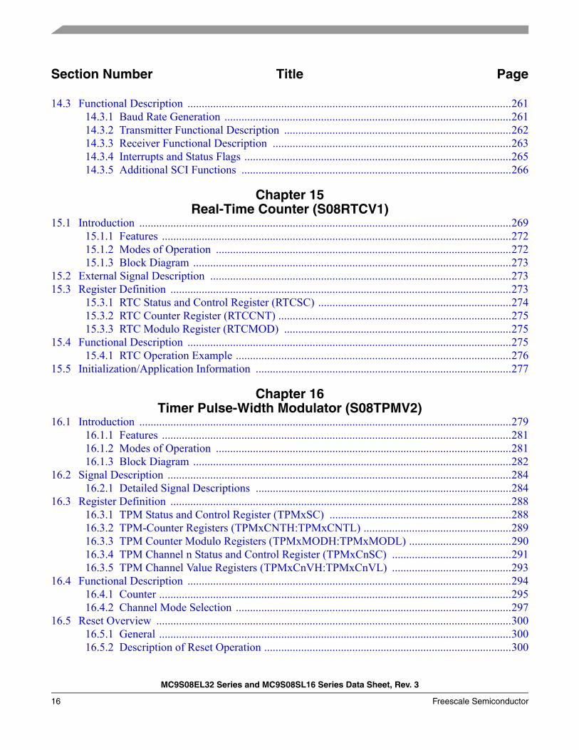
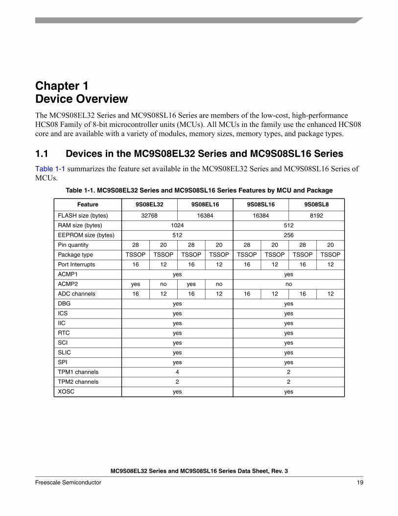
1.1 Devices in the MC9S08EL32 Series and MC9S08SL16 SeriesTable 1-1 summarizes the feature set available in the MC9S08EL32 Series and MC9S08SL16 Series of MCUs.
t
Table 1-1. MC9S08EL32 Series and MC9S08SL16 Series Features by MCU and Package
Feature 9S08EL32 9S08EL16 9S08SL16 9S08SL8
FLASH size (bytes) 32768 16384 16384 8192
RAM size (bytes) 1024 512
EEPROM size (bytes) 512 256
Pin quantity 28 20 28 20 28 20 28 20
Package type TSSOP TSSOP TSSOP TSSOP TSSOP TSSOP TSSOP TSSOP
Port Interrupts 16 12 16 12 16 12 16 12
ACMP1 yes yes
ACMP2 yes no yes no no
ADC channels 16 12 16 12 16 12 16 12
DBG yes yes
ICS yes yes
IIC yes yes
RTC yes yes
SCI yes yes
SLIC yes yes
SPI yes yes
TPM1 channels 4 2
TPM2 channels 2 2
XOSC yes yes
Chapter 1 Device Overview
MC9S08EL32 Series and MC9S08SL16 Series Data Sheet, Rev. 3
20 Freescale Semiconductor
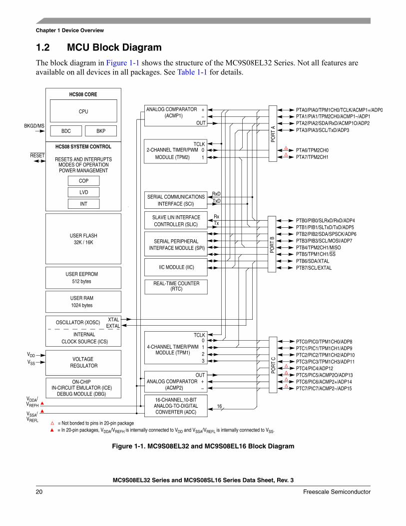
1.2 MCU Block DiagramThe block diagram in Figure 1-1 shows the structure of the MC9S08EL32 Series. Not all features are available on all devices in all packages. See Table 1-1 for details.
Figure 1-1. MC9S08EL32 and MC9S08EL16 Block Diagram
VSS
IIC MODULE (IIC)
SERIAL PERIPHERAL INTERFACE MODULE (SPI)
USER FLASH
USER RAM
32K / 16K
HCS08 CORE
CPU
BDC
2-CHANNEL TIMER/PWMMODULE (TPM2)
HCS08 SYSTEM CONTROL
RESETS AND INTERRUPTSMODES OF OPERATIONPOWER MANAGEMENT
VOLTAGE REGULATOR
COP
LVD
OSCILLATOR (XOSC)
INTERNALCLOCK SOURCE (ICS)
RESET
VREFH
1024 bytes
INTERFACE (SCI)SERIAL COMMUNICATIONS
XTALEXTAL
4-CHANNEL TIMER/PWMMODULE (TPM1)
REAL-TIME COUNTER
IN-CIRCUIT EMULATOR (ICE)
BKGD/MS PTA3/PIA3/SCL/TxD/ADP3
PTA6/TPM2CH0
PTA2/PIA2/SDA/RxD/ACMP1O/ADP2PTA1/PIA1/TPM2CH0/ACMP1–/ADP1PTA0/PIA0/TPM1CH0/TCLK/ACMP1+/ADP0
PTA7/TPM2CH1
PTB3/PIB3/SCL/MOSI/ADP7PTB4/TPM2CH1/MISO
PTB2/PIB2/SDA/SPSCK/ADP6PTB1/PIB1/SLTxD/TxD/ADP5PTB0/PIB0/SLRxD/RxD/ADP4
PTB7/SCL/EXTAL
PTC3/PIC3/TPM1CH3/ADP11PTC4/PIC4/ADP12PTC5/PIC5/ACMP2O/ADP13
PTC2/PIC2/TPM1CH2/ADP10PTC1/PIC1/TPM1CH1/ADP9
POR
T C
PTC6/PIC6/ACMP2+/ADP14
VDD
BKP
INT
ANALOG COMPARATOR(ACMP2)
USER EEPROM512 bytes
CONTROLLER (SLIC)SLAVE LIN INTERFACE
ANALOG-TO-DIGITALCONVERTER (ADC)
16-CHANNEL,10-BIT16
= In 20-pin packages, VDDA/VREFH is internally connected to VDD and VSSA/VREFL is internally connected to VSS.
VDDA/
VREFL
VSSA/
DEBUG MODULE (DBG)
ON-CHIP
(RTC)
PTC0/PIC0/TPM1CH0/ADP8
PTC7/PIC7/ACMP2–/ADP15
PTB6/SDA/XTAL
POR
T B
POR
T A
PTB5/TPM1CH1/SS
ANALOG COMPARATOR(ACMP1)
= Not bonded to pins in 20-pin package
TCLK
TCLK
+–
OUT
+–
OUT
0123
10
RxDTxD
TxRx
Chapter 1 Device Overview
MC9S08EL32 Series and MC9S08SL16 Series Data Sheet, Rev. 3
Freescale Semiconductor 21
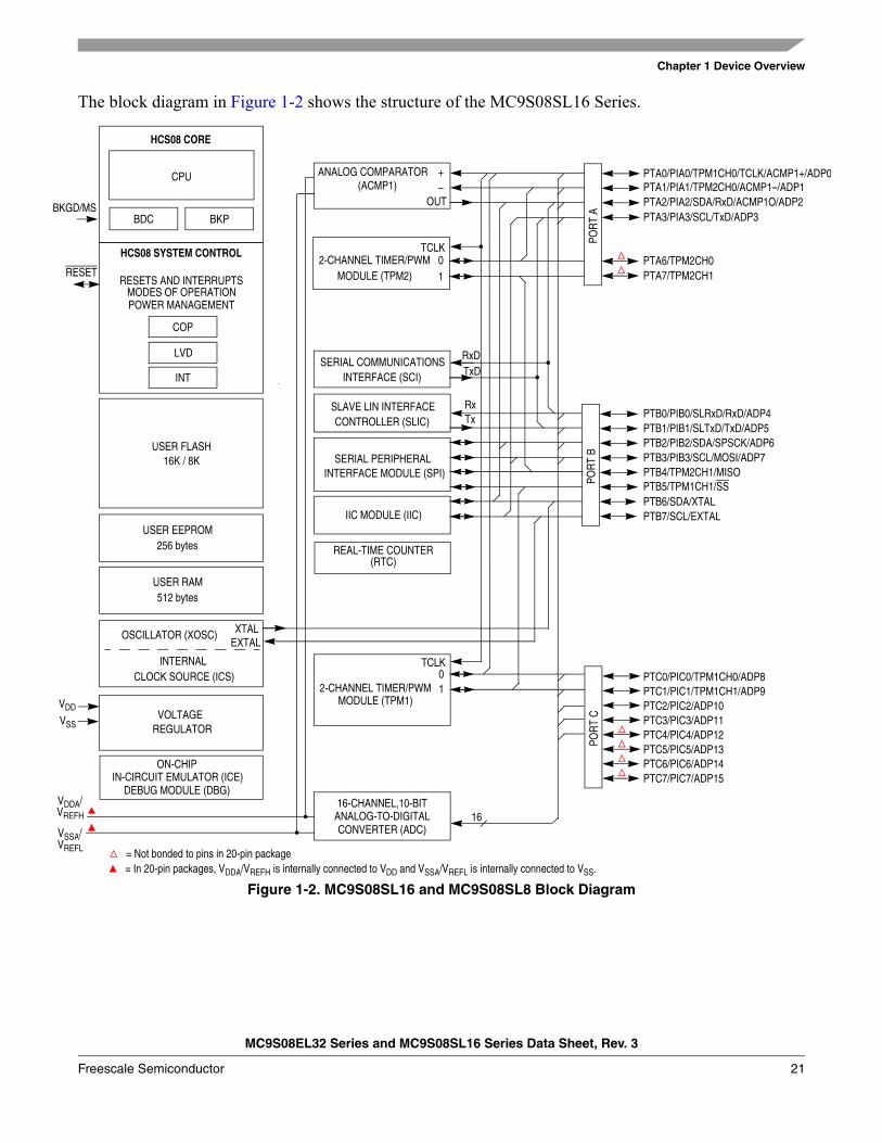
The block diagram in Figure 1-2 shows the structure of the MC9S08SL16 Series.
Figure 1-2. MC9S08SL16 and MC9S08SL8 Block Diagram
VSS
IIC MODULE (IIC)
SERIAL PERIPHERAL INTERFACE MODULE (SPI)
USER FLASH
USER RAM
16K / 8K
HCS08 CORE
CPU
BDC
2-CHANNEL TIMER/PWMMODULE (TPM2)
HCS08 SYSTEM CONTROL
RESETS AND INTERRUPTSMODES OF OPERATIONPOWER MANAGEMENT
VOLTAGE REGULATOR
COP
LVD
OSCILLATOR (XOSC)
INTERNALCLOCK SOURCE (ICS)
RESET
VREFH
512 bytes
INTERFACE (SCI)SERIAL COMMUNICATIONS
XTALEXTAL
2-CHANNEL TIMER/PWMMODULE (TPM1)
REAL-TIME COUNTER
IN-CIRCUIT EMULATOR (ICE)
BKGD/MS PTA3/PIA3/SCL/TxD/ADP3
PTA6/TPM2CH0
PTA2/PIA2/SDA/RxD/ACMP1O/ADP2PTA1/PIA1/TPM2CH0/ACMP1–/ADP1PTA0/PIA0/TPM1CH0/TCLK/ACMP1+/ADP0
PTA7/TPM2CH1
PTB3/PIB3/SCL/MOSI/ADP7PTB4/TPM2CH1/MISO
PTB2/PIB2/SDA/SPSCK/ADP6PTB1/PIB1/SLTxD/TxD/ADP5PTB0/PIB0/SLRxD/RxD/ADP4
PTB7/SCL/EXTAL
PTC3/PIC3/ADP11PTC4/PIC4/ADP12PTC5/PIC5/ADP13
PTC2/PIC2/ADP10PTC1/PIC1/TPM1CH1/ADP9
POR
T C
PTC6/PIC6/ADP14
VDD
BKP
INT
USER EEPROM256 bytes
CONTROLLER (SLIC)SLAVE LIN INTERFACE
ANALOG-TO-DIGITALCONVERTER (ADC)
16-CHANNEL,10-BIT16
= In 20-pin packages, VDDA/VREFH is internally connected to VDD and VSSA/VREFL is internally connected to VSS.
VDDA/
VREFL
VSSA/
DEBUG MODULE (DBG)
ON-CHIP
(RTC)
PTC0/PIC0/TPM1CH0/ADP8
PTC7/PIC7/ADP15
PTB6/SDA/XTAL
POR
T B
POR
T A
PTB5/TPM1CH1/SS
ANALOG COMPARATOR(ACMP1)
= Not bonded to pins in 20-pin package
TCLK
TCLK
+–
OUT
01
10
RxDTxD
TxRx
Chapter 1 Device Overview
MC9S08EL32 Series and MC9S08SL16 Series Data Sheet, Rev. 3
22 Freescale Semiconductor
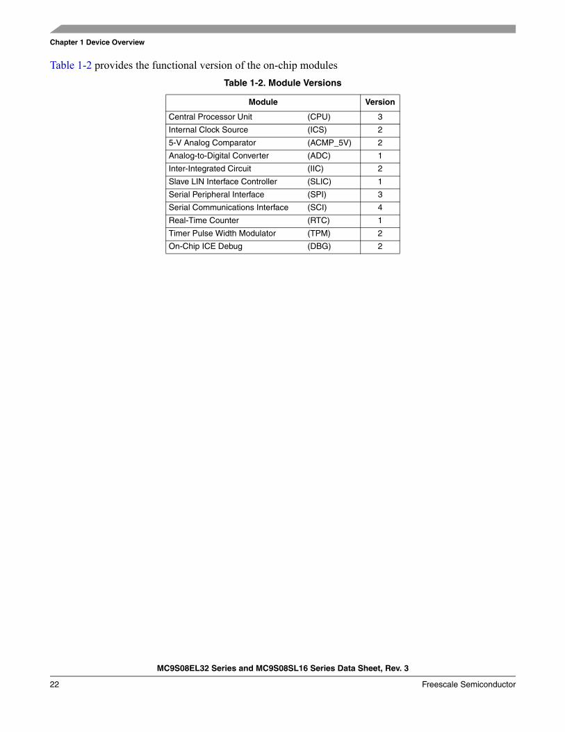
Table 1-2 provides the functional version of the on-chip modulesTable 1-2. Module Versions
Module Version
Central Processor Unit (CPU) 3
Internal Clock Source (ICS) 2
5-V Analog Comparator (ACMP_5V) 2
Analog-to-Digital Converter (ADC) 1
Inter-Integrated Circuit (IIC) 2
Slave LIN Interface Controller (SLIC) 1
Serial Peripheral Interface (SPI) 3
Serial Communications Interface (SCI) 4
Real-Time Counter (RTC) 1
Timer Pulse Width Modulator (TPM) 2
On-Chip ICE Debug (DBG) 2
Chapter 1 Device Overview
MC9S08EL32 Series and MC9S08SL16 Series Data Sheet, Rev. 3
Freescale Semiconductor 23
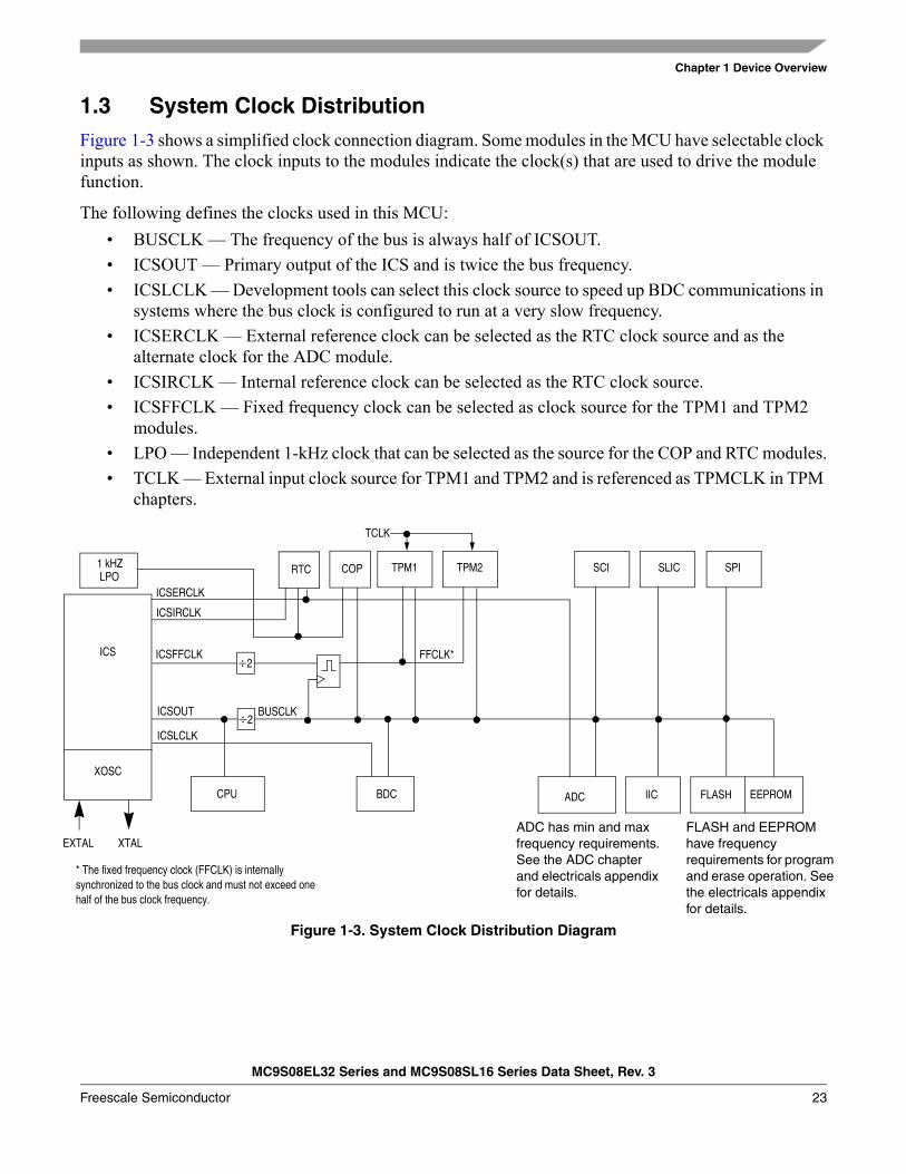
1.3 System Clock DistributionFigure 1-3 shows a simplified clock connection diagram. Some modules in the MCU have selectable clock inputs as shown. The clock inputs to the modules indicate the clock(s) that are used to drive the module function.
The following defines the clocks used in this MCU:• BUSCLK — The frequency of the bus is always half of ICSOUT.• ICSOUT — Primary output of the ICS and is twice the bus frequency. • ICSLCLK — Development tools can select this clock source to speed up BDC communications in
systems where the bus clock is configured to run at a very slow frequency.• ICSERCLK — External reference clock can be selected as the RTC clock source and as the
alternate clock for the ADC module.• ICSIRCLK — Internal reference clock can be selected as the RTC clock source.• ICSFFCLK — Fixed frequency clock can be selected as clock source for the TPM1 and TPM2
modules.• LPO — Independent 1-kHz clock that can be selected as the source for the COP and RTC modules.• TCLK — External input clock source for TPM1 and TPM2 and is referenced as TPMCLK in TPM
chapters.
Figure 1-3. System Clock Distribution Diagram
TPM1 TPM2 SCI SLIC
BDCCPU ADC IIC FLASH
ICS
ICSOUT ÷2 BUSCLK
ICSLCLK
ICSERCLK
COP
* The fixed frequency clock (FFCLK) is internally synchronized to the bus clock and must not exceed one half of the bus clock frequency.
FLASH and EEPROM have frequency requirements for program and erase operation. See the electricals appendix for details.
ADC has min and maxfrequency requirements.See the ADC chapter and electricals appendix for details.
XOSC
EXTAL XTAL
EEPROM
SPI
FFCLK*ICSFFCLK
RTC 1 kHZLPO
TCLK
ICSIRCLK
÷2

Chapter 1 Device Overview
MC9S08EL32 Series and MC9S08SL16 Series Data Sheet, Rev. 3
24 Freescale Semiconductor
MC9S08EL32 Series and MC9S08SL16 Series Data Sheet, Rev. 3
Freescale Semiconductor 25
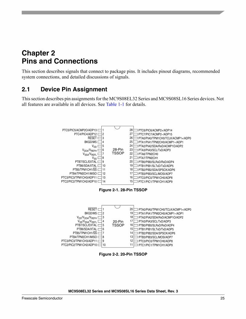
Chapter 2 Pins and ConnectionsThis section describes signals that connect to package pins. It includes pinout diagrams, recommended system connections, and detailed discussions of signals.
2.1 Device Pin AssignmentThis section describes pin assignments for the MC9S08EL32 Series and MC9S08SL16 Series devices. Not all features are available in all devices. See Table 1-1 for details.
Figure 2-1. 28-Pin TSSOP
Figure 2-2. 20-Pin TSSOP
1234567891011121314
PTC6/PIC6/ACMP2+/ADP14PTC7/PIC7/ACMP2–/ADP15PTA0/PIA0/TPM1CH0/TCLK/ACMP1+/ADP0PTA1/PIA1/TPM2CH0/ACMP1–/ADP1PTA2/PIA2/SDA/RxD/ACMP1O/ADP2PTA3/PIA3/SCL/TxD/ADP3PTA6/TPM2CH0PTA7/TPM2CH1PTB0/PIB0/SLRxD/RxD/ADP4PTB1/PIB1/SLTxD/TxD/ADP5PTB2/PIB2/SDA/SPSCK/ADP6PTB3/PIB3/SCL/MOSI/ADP7PTC0/PIC0/TPM1CH0/ADP8PTC1/PIC1/TPM1CH1/ADP9
PTC5/PIC5/ACMP2O/ADP13PTC4/PIC4/ADP12
RESETBKGD/MS
VDDVDDA/VREFHVSSA/VREFL
VSSPTB7/SCL/EXTALPTB6/SDA/XTAL
PTB5/TPM1CH1/SSPTB4/TPM2CH1/MISO
PTC3/PIC3/TPM1CH3/ADP11PTC2/PIC2/TPM1CH2/ADP10
2827262524232221201918171615
28-PinTSSOP
12345678910
PTA0/PIA0/TPM1CH0/TCLK/ACMP1+/ADP0PTA1/PIA1/TPM2CH0/ACMP1–/ADP1PTA2/PIA2/SDA/RxD/ACMP1O/ADP2PTA3/PIA3/SCL/TxD/ADP3PTB0/PIB0/SLRxD/RxD/ADP4PTB1/PIB1/SLTxD/TxD/ADP5PTB2/PIB2/SDA/SPSCK/ADP6PTB3/PIB3/SCL/MOSI/ADP7PTC0/PIC0/TPM1CH0/ADP8PTC1/PIC1/TPM1CH1/ADP9
RESETBKGD/MS
VDD/VDDA/VREFHVSS/VSSA/VREFL
PTB7/SCL/EXTALPTB6/SDA/XTAL
PTB5/TPM1CH1/SSPTB4/TPM2CH1/MISO
PTC3/PIC3/TPM1CH3/ADP11PTC2/PIC2/TPM1CH2/ADP10
20191817161514131211
20-PinTSSOP
Chapter 2 Pins and Connections
MC9S08EL32 Series and MC9S08SL16 Series Data Sheet, Rev. 3
26 Freescale Semiconductor
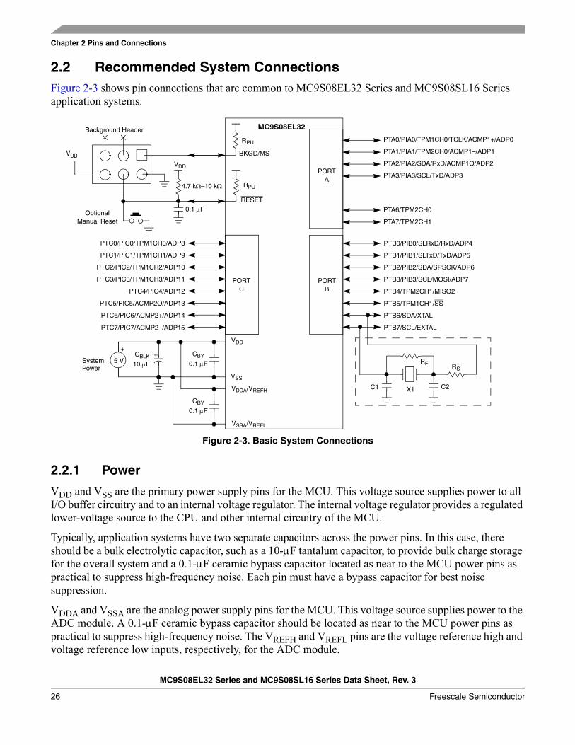
2.2 Recommended System ConnectionsFigure 2-3 shows pin connections that are common to MC9S08EL32 Series and MC9S08SL16 Series application systems.
Figure 2-3. Basic System Connections
2.2.1 Power
VDD and VSS are the primary power supply pins for the MCU. This voltage source supplies power to all I/O buffer circuitry and to an internal voltage regulator. The internal voltage regulator provides a regulated lower-voltage source to the CPU and other internal circuitry of the MCU.
Typically, application systems have two separate capacitors across the power pins. In this case, there should be a bulk electrolytic capacitor, such as a 10-μF tantalum capacitor, to provide bulk charge storage for the overall system and a 0.1-μF ceramic bypass capacitor located as near to the MCU power pins as practical to suppress high-frequency noise. Each pin must have a bypass capacitor for best noise suppression.
VDDA and VSSA are the analog power supply pins for the MCU. This voltage source supplies power to the ADC module. A 0.1-μF ceramic bypass capacitor should be located as near to the MCU power pins as practical to suppress high-frequency noise. The VREFH and VREFL pins are the voltage reference high and voltage reference low inputs, respectively, for the ADC module.
BKGD/MS
RESET
OptionalManual Reset
VDD
Background Header
SystemPower
PORTB
PTB0/PIB0/SLRxD/RxD/ADP4
PTB1/PIB1/SLTxD/TxD/ADP5
PTB2/PIB2/SDA/SPSCK/ADP6
PTB3/PIB3/SCL/MOSI/ADP7
PTB4/TPM2CH1/MISO2
PTB5/TPM1CH1/SS
PTB6/SDA/XTAL
PTB7/SCL/EXTAL
PORTC
PTC0/PIC0/TPM1CH0/ADP8
PTC1/PIC1/TPM1CH1/ADP9
PTC2/PIC2/TPM1CH2/ADP10
PTC3/PIC3/TPM1CH3/ADP11
PTC4/PIC4/ADP12
PTC5/PIC5/ACMP2O/ADP13
PTC6/PIC6/ACMP2+/ADP14
MC9S08EL32
VDDA/VREFH
VSSA/VREFL
VSS
VDD
PTC7/PIC7/ACMP2–/ADP15
CBY
0.1 μF
CBLK
10 μF
+5 V
+
C2C1 X1
RF RS
PORTA
PTA0/PIA0/TPM1CH0/TCLK/ACMP1+/ADP0
PTA1/PIA1/TPM2CH0/ACMP1–/ADP1
PTA2/PIA2/SDA/RxD/ACMP1O/ADP2
PTA3/PIA3/SCL/TxD/ADP3
PTA6/TPM2CH0
PTA7/TPM2CH1
VDD
4.7 kΩ–10 kΩ
0.1 μF
RPU
RPU
CBY
0.1 μF
Chapter 2 Pins and Connections
MC9S08EL32 Series and MC9S08SL16 Series Data Sheet, Rev. 3
Freescale Semiconductor 27
2.2.2 Oscillator
Immediately after reset, the MCU uses an internally generated clock provided by the clock source generator (ICS) module. This internal clock source is used during reset startup and can be enabled as the clock source for stop recovery to avoid the need for a long crystal startup delay. For more information on the ICS, see Chapter 8, “Internal Clock Source (S08ICSV2).”
The oscillator (XOSC) in this MCU is a Pierce oscillator that can accommodate a crystal or ceramic resonator. Rather than a crystal or ceramic resonator, an external oscillator can be connected to the EXTAL input pin.
Refer to Figure 2-3 for the following discussion. RS (when used) and RF should be low-inductance resistors such as carbon composition resistors. Wire-wound resistors, and some metal film resistors, have too much inductance. C1 and C2 normally should be high-quality ceramic capacitors that are specifically designed for high-frequency applications.
RF is used to provide a bias path to keep the EXTAL input in its linear range during crystal startup; its value is not generally critical. Typical systems use 1 MΩ to 10 MΩ. Higher values are sensitive to humidity and lower values reduce gain and (in extreme cases) could prevent startup.
C1 and C2 are typically in the 5-pF to 25-pF range and are chosen to match the requirements of a specific crystal or resonator. Be sure to take into account printed circuit board (PCB) capacitance and MCU pin capacitance when selecting C1 and C2. The crystal manufacturer typically specifies a load capacitance which is the series combination of C1 and C2 (which are usually the same size). As a first-order approximation, use 10 pF as an estimate of combined pin and PCB capacitance for each oscillator pin (EXTAL and XTAL).
2.2.3 RESET
RESET is a dedicated pin with a built in pull-up device. It has input hysteresis and an open drain output. Since the pin does not have a clamp diode to VDD, it should not be driven above VDD. Internal power-on reset and low-voltage reset circuitry typically make external reset circuitry unnecessary. This pin is normally connected to the standard 6-pin background debug connector so a development system can directly reset the MCU system. If desired, a manual external reset can be added by supplying a simple switch to ground (pull reset pin low to force a reset).
Whenever any reset is initiated (whether from an external signal or from an internal system), the RESET pin is driven low for about 66 bus cycles. The reset circuitry decodes the cause of reset and records it by setting a corresponding bit in the system reset status register (SRS).
NOTEThis pin does not contain a clamp diode to VDD and should not be driven above VDD. The voltage measured on the internally-pulled-up RESET pin is not pulled to VDD. The internal gates connected to this pin are pulled to VDD. If the RESET pin is required to drive to a VDD level, use an external pullup.
Chapter 2 Pins and Connections
MC9S08EL32 Series and MC9S08SL16 Series Data Sheet, Rev. 3
28 Freescale Semiconductor
NOTEIn EMC-sensitive applications, use an external RC filter on RESET. See Figure 2-3 for an example.
2.2.4 Background / Mode Select (BKGD/MS)
While in reset, the BKGD/MS pin functions as a mode select pin. Immediately after reset rises, the pin functions as the background pin and can be used for background debug communication. While functioning as a background or mode select pin, the pin includes an internal pull-up device, input hysteresis, a standard output driver, and no output slew rate control.
If nothing is connected to this pin, the MCU will enter normal operating mode at the rising edge of reset. If a debug system is connected to the 6-pin standard background debug header, it can hold BKGD low during the rising edge of reset which forces the MCU to active background mode.
The BKGD/MS pin is used primarily for background debug controller (BDC) communications using a custom protocol that uses 16 clock cycles of the target MCU’s BDC clock per bit time. The target MCU’s BDC clock could be as fast as the bus clock rate, so there should never be any significant capacitance connected to the BKGD/MS pin that could interfere with background serial communications.
Although the BKGD/MS pin is a pseudo open-drain pin, the background debug communication protocol provides brief, actively driven, high speedup pulses to ensure fast rise times. Small capacitances from cables and the absolute value of the internal pull-up device play almost no role in determining rise and fall times on the BKGD/MS pin.
2.2.5 General-Purpose I/O and Peripheral Ports
The MC9S08EL32 Series and MC9S08SL16 Series of MCUs support up to 22 general-purpose I/O pins which are shared with on-chip peripheral functions (timers, serial I/O, ADC, etc.).
When a port pin is configured as a general-purpose output or a peripheral uses the port pin as an output, software can select one of two drive strengths and enable or disable slew rate control. When a port pin is configured as a general-purpose input or a peripheral uses the port pin as an input, software can enable a pull-up device. Immediately after reset, all of these pins are configured as high-impedance general-purpose inputs with internal pull-up devices disabled.
When an on-chip peripheral system is controlling a pin, data direction control bits still determine what is read from port data registers even though the peripheral module controls the pin direction by controlling the enable for the pin’s output buffer. For information about controlling these pins as general-purpose I/O pins, see Chapter 6, “Parallel Input/Output Control.”
NOTETo avoid extra current drain from floating input pins, the reset initialization routine in the application program should either enable on-chip pull-up devices or change the direction of unused or non-bonded pins to outputs so they do not float.
Chapter 2 Pins and Connections
MC9S08EL32 Series and MC9S08SL16 Series Data Sheet, Rev. 3
Freescale Semiconductor 29
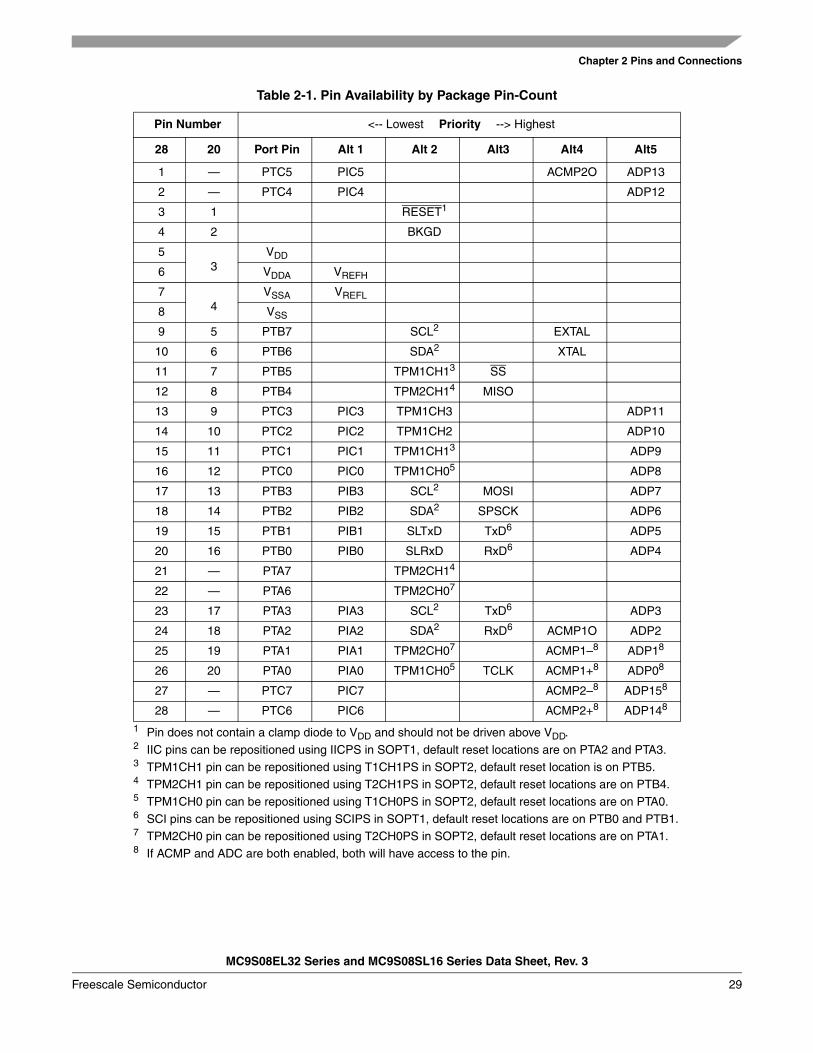
Table 2-1. Pin Availability by Package Pin-Count
Pin Number <-- Lowest Priority --> Highest
28 20 Port Pin Alt 1 Alt 2 Alt3 Alt4 Alt5
1 — PTC5 PIC5 ACMP2O ADP13
2 — PTC4 PIC4 ADP12
3 1 RESET1
1 Pin does not contain a clamp diode to VDD and should not be driven above VDD.
4 2 BKGD
53
VDD
6 VDDA VREFH
74
VSSA VREFL
8 VSS
9 5 PTB7 SCL2
2 IIC pins can be repositioned using IICPS in SOPT1, default reset locations are on PTA2 and PTA3.
EXTAL
10 6 PTB6 SDA2 XTAL
11 7 PTB5 TPM1CH13
3 TPM1CH1 pin can be repositioned using T1CH1PS in SOPT2, default reset location is on PTB5.
SS
12 8 PTB4 TPM2CH14
4 TPM2CH1 pin can be repositioned using T2CH1PS in SOPT2, default reset locations are on PTB4.
MISO
13 9 PTC3 PIC3 TPM1CH3 ADP11
14 10 PTC2 PIC2 TPM1CH2 ADP10
15 11 PTC1 PIC1 TPM1CH13 ADP9
16 12 PTC0 PIC0 TPM1CH05
5 TPM1CH0 pin can be repositioned using T1CH0PS in SOPT2, default reset locations are on PTA0.
ADP8
17 13 PTB3 PIB3 SCL2 MOSI ADP7
18 14 PTB2 PIB2 SDA2 SPSCK ADP6
19 15 PTB1 PIB1 SLTxD TxD6
6 SCI pins can be repositioned using SCIPS in SOPT1, default reset locations are on PTB0 and PTB1.
ADP5
20 16 PTB0 PIB0 SLRxD RxD6 ADP4
21 — PTA7 TPM2CH14
22 — PTA6 TPM2CH07
7 TPM2CH0 pin can be repositioned using T2CH0PS in SOPT2, default reset locations are on PTA1.
23 17 PTA3 PIA3 SCL2 TxD6 ADP3
24 18 PTA2 PIA2 SDA2 RxD6 ACMP1O ADP2
25 19 PTA1 PIA1 TPM2CH07 ACMP1–8
8 If ACMP and ADC are both enabled, both will have access to the pin.
ADP18
26 20 PTA0 PIA0 TPM1CH05 TCLK ACMP1+8 ADP08
27 — PTC7 PIC7 ACMP2–8 ADP158
28 — PTC6 PIC6 ACMP2+8 ADP148

Chapter 2 Pins and Connections
MC9S08EL32 Series and MC9S08SL16 Series Data Sheet, Rev. 3
30 Freescale Semiconductor
MC9S08EL32 Series and MC9S08SL16 Series Data Sheet, Rev. 3
Freescale Semiconductor 31
Chapter 3 Modes of Operation
3.1 IntroductionThe operating modes of the MC9S08EL32 Series and MC9S08SL16 Series are described in this chapter. Entry into each mode, exit from each mode, and functionality while in each of the modes is described.
3.2 Features• Active background mode for code development• Wait mode — CPU shuts down to conserve power; system clocks are running and full regulation
is maintained• Stop modes — System clocks are stopped and voltage regulator is in standby
— Stop3 — All internal circuits are powered for fast recovery; RAM and register contents are retained
— Stop2 — Partial power down of internal circuits; RAM content is retained
3.3 Run ModeThis is the normal operating mode for the MC9S08EL32 Series and MC9S08SL16 Series. This mode is selected when the BKGD/MS pin is high at the rising edge of reset. In this mode, the CPU executes code from internal memory with execution beginning at the address fetched from memory at 0xFFFE–0xFFFF after reset.
3.4 Active Background ModeThe active background mode functions are managed through the background debug controller (BDC) in the HCS08 core. The BDC, together with the on-chip debug module (DBG), provide the means for analyzing MCU operation during software development.
Active background mode is entered in any of five ways: • When the BKGD/MS pin is low at the rising edge of reset• When a BACKGROUND command is received through the BKGD/MS pin• When a BGND instruction is executed• When encountering a BDC breakpoint• When encountering a DBG breakpoint
After entering active background mode, the CPU is held in a suspended state waiting for serial background commands rather than executing instructions from the user application program.
Chapter 3 Modes of Operation
MC9S08EL32 Series and MC9S08SL16 Series Data Sheet, Rev. 3
32 Freescale Semiconductor
Background commands are of two types:• Non-intrusive commands, defined as commands that can be issued while the user program is
running. Non-intrusive commands can be issued through the BKGD/MS pin while the MCU is in run mode; non-intrusive commands can also be executed when the MCU is in the active background mode. Non-intrusive commands include:— Memory access commands— Memory-access-with-status commands— BDC register access commands— The BACKGROUND command
• Active background commands, which can only be executed while the MCU is in active background mode. Active background commands include commands to:— Read or write CPU registers— Trace one user program instruction at a time— Leave active background mode to return to the user application program (GO)
The active background mode is used to program a bootloader or user application program into the FLASH program memory before the MCU is operated in run mode for the first time. When the MC9S08EL32 Series and MC9S08SL16 Series is shipped from the Freescale Semiconductor factory, the FLASH program memory is erased by default unless specifically noted so there is no program that could be executed in run mode until the FLASH memory is initially programmed. The active background mode can also be used to erase and reprogram the FLASH memory after it has been previously programmed.
For additional information about the active background mode, refer to the Development Support chapter.
3.5 Wait ModeWait mode is entered by executing a WAIT instruction. Upon execution of the WAIT instruction, the CPU enters a low-power state in which it is not clocked. The I bit in CCR is cleared when the CPU enters the wait mode, enabling interrupts. When an interrupt request occurs, the CPU exits the wait mode and resumes processing, beginning with the stacking operations leading to the interrupt service routine.
While the MCU is in wait mode, there are some restrictions on which background debug commands can be used. Only the BACKGROUND command and memory-access-with-status commands are available when the MCU is in wait mode. The memory-access-with-status commands do not allow memory access, but they report an error indicating that the MCU is in either stop or wait mode. The BACKGROUND command can be used to wake the MCU from wait mode and enter active background mode.
3.6 Stop ModesOne of two stop modes is entered upon execution of a STOP instruction when the STOPE bit in SOPT1 register is set. In both stop modes, all internal clocks are halted. The ICS module can be configured to leave the reference clocks running. See Chapter 8, “Internal Clock Source (S08ICSV2),” for more information.
Chapter 3 Modes of Operation
MC9S08EL32 Series and MC9S08SL16 Series Data Sheet, Rev. 3
Freescale Semiconductor 33
Table 3-1 shows all of the control bits that affect stop mode selection and the mode selected under various conditions. The selected mode is entered following the execution of a STOP instruction.
3.6.1 Stop3 Mode
Stop3 mode is entered by executing a STOP instruction under the conditions as shown in Table 3-1. The states of all of the internal registers and logic, RAM contents, and I/O pin states are maintained.
Exit from stop3 is done by asserting RESET, or an asynchronous interrupt pin. The asynchronous interrupt pins are PIA0-PIA3, PIB0 -PIB3, and PIC0-PIC7. Exit from stop3 can also be done by the low-voltage detection (LVD) reset, the low-voltage warning (LVW) interrupt, the ADC conversion complete interrupt, the analog comparator (ACMP) interrupt, the real-time counter (RTC) interrupt, the SLIC wake-up interrupt, or the SCI receiver interrupt.
If stop3 is exited by means of the RESET pin, the MCU will be reset and operation will resume after fetching the reset vector. Exit by means of an asynchronous interrupt, analog comparator interrupt, or the real-time interrupt will result in the MCU fetching the appropriate interrupt vector.
3.6.1.1 LVD Enabled in Stop Mode
The LVD system is capable of generating either an interrupt or a reset when the supply voltage drops below the LVD voltage. If the LVD is enabled in stop (LVDE and LVDSE bits in SPMSC1 both set) at the time the CPU executes a STOP instruction, then the voltage regulator remains active during stop mode.
For the ADC to operate the LVD must be left enabled when entering stop3.
3.6.1.2 Active BDM Enabled in Stop Mode
Entry into the active background mode from run mode is enabled if ENBDM in BDCSCR is set. This register is described in Chapter 17, “Development Support.” If ENBDM is set when the CPU executes a STOP instruction, the system clocks to the background debug logic remain active when the MCU enters stop mode. Because of this, background debug communication remains possible. In addition, the voltage regulator does not enter its low-power standby state but maintains full internal regulation.
Table 3-1. Stop Mode Selection
STOPE ENBDM 1
1 ENBDM is located in the BDCSCR, which is only accessible through BDC commands, see Section 17.4.1.1, “BDC Status and Control Register (BDCSCR)”.
LVDE LVDSE PPDC Stop Mode
0 x x x Stop modes disabled; illegal opcode reset if STOP instruction executed
1 1 x x Stop3 with BDM enabled 2
2 When in Stop3 mode with BDM enabled, The SIDD will be near RIDD levels because internal clocks are enabled.
1 0 Both bits must be 1 0 Stop3 with voltage regulator active
1 0 Either bit a 0 0 Stop3
1 0 Either bit a 0 1 Stop2
Chapter 3 Modes of Operation
MC9S08EL32 Series and MC9S08SL16 Series Data Sheet, Rev. 3
34 Freescale Semiconductor
Most background commands are not available in stop mode. The memory-access-with-status commands do not allow memory access, but they report an error indicating that the MCU is in either stop or wait mode. The BACKGROUND command can be used to wake the MCU from stop and enter active background mode if the ENBDM bit is set. After entering background debug mode, all background commands are available.
3.7 Stop2 ModeStop2 mode is entered by executing a STOP instruction under the conditions as shown in Table 3-1. Most of the internal circuitry of the MCU is powered off in stop2 with the exception of the RAM. Upon entering stop2, all I/O pin control signals are latched so that the pins retain their states during stop2.
Exit from stop2 is performed by asserting RESET on the MCU. In addition, the real-time counter (RTC) can wake the MCU from stop2, if enabled.
Upon wake-up from stop2 mode, the MCU starts up as from a power-on reset (POR): • All module control and status registers are reset• The LVD reset function is enabled and the MCU remains in the reset state if VDD is below the LVD
trip point (low trip point selected due to POR)• The CPU takes the reset vector
In addition to the above, upon waking up from stop2, the PPDF bit in SPMSC2 is set. This flag is used to direct user code to go to a stop2 recovery routine. PPDF remains set and the I/O pin states remain latched until a 1 is written to PPDACK in SPMSC2.
To maintain I/O states for pins that were configured as general-purpose I/O before entering stop2, the user must restore the contents of the I/O port registers, which have been saved in RAM, to the port registers before writing to the PPDACK bit. If the port registers are not restored from RAM before writing to PPDACK, then the pins will switch to their reset states when PPDACK is written.
For pins that were configured as peripheral I/O, the user must reconfigure the peripheral module that interfaces to the pin before writing to the PPDACK bit. If the peripheral module is not enabled before writing to PPDACK, the pins will be controlled by their associated port control registers when the I/O latches are opened.
3.8 On-Chip Peripheral Modules in Stop ModesWhen the MCU enters any stop mode, system clocks to the internal peripheral modules are stopped. Even in the exception case (ENBDM = 1), where clocks to the background debug logic continue to operate, clocks to the peripheral systems are halted to reduce power consumption. Refer to Section 3.7, “Stop2 Mode” and Section 3.6.1, “Stop3 Mode” for specific information on system behavior in stop modes.
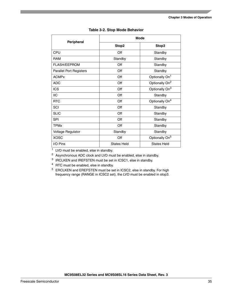
Chapter 3 Modes of Operation
MC9S08EL32 Series and MC9S08SL16 Series Data Sheet, Rev. 3
Freescale Semiconductor 35
Table 3-2. Stop Mode Behavior
PeripheralMode
Stop2 Stop3
CPU Off Standby
RAM Standby Standby
FLASH/EEPROM Off Standby
Parallel Port Registers Off Standby
ACMPx Off Optionally On1
1 LVD must be enabled, else in standby.
ADC Off Optionally On2
2 Asynchronous ADC clock and LVD must be enabled, else in standby.
ICS Off Optionally On3
3 IRCLKEN and IREFSTEN must be set in ICSC1, else in standby.
IIC Off Standby
RTC Off Optionally On4
4 RTC must be enabled, else in standby.
SCI Off Standby
SLIC Off Standby
SPI Off Standby
TPMx Off Standby
Voltage Regulator Standby Standby
XOSC Off Optionally On5
5 ERCLKEN and EREFSTEN must be set in ICSC2, else in standby. For high frequency range (RANGE in ICSC2 set), the LVD must be enabled in stop3.
I/O Pins States Held States Held

Chapter 3 Modes of Operation
MC9S08EL32 Series and MC9S08SL16 Series Data Sheet, Rev. 3
36 Freescale Semiconductor

MC9S08EL32 Series and MC9S08SL16 Series Data Sheet, Rev. 3
Freescale Semiconductor 37
Chapter 4 Memory
4.1 MC9S08EL32 Series and MC9S08SL16 Series Memory MapAs shown in Figure 4-1, on-chip memory in the MC9S08EL32 Series and MC9S08SL16 Series consists of RAM, EEPROM, and FLASH program memory for nonvolatile data storage, and I/O and control/status registers. The registers are divided into three groups:
• Direct-page registers (0x0000 through 0x007F)• High-page registers (0x1800 through 0x18FF)• Nonvolatile registers (0xFFB0 through 0xFFBF)
Figure 4-1. MC9S08EL32 Series and MC9S08SL16 Series Memory Map
DIRECT PAGE REGISTERS
RAM1024 BYTES
0x0000
0x007F0x0080
0x047F
0x18000x17FF
0x18FF0x1900
0xFFFF
0x1700
MC9S08EL32
0x7FFF0x8000
128 BYTES
HIGH PAGE REGISTERS256 BYTES
FLASH32768 BYTES
UNIMPLEMENTED
0x0480
0x16FF
4736 BYTES
UNIMPLEMENTED26368 BYTES
EEPROM2 x 256 BYTES
DIRECT PAGE REGISTERS
RAM1024 BYTES
0x0000
0x007F0x0080
0x047F
0x18000x17FF
0x18FF0x1900
0xFFFF
0x1700
MC9S08EL16
0x7FFF0x8000
128 BYTES
HIGH PAGE REGISTERS256 BYTES
FLASH16384 BYTES
UNIMPLEMENTED
0x0480
0x16FF
4736 BYTES
UNIMPLEMENTED26368 BYTES
EEPROM2 x 256 BYTES
RESERVED
0xBFFF0xC000
16384 BYTES
DIRECT PAGE REGISTERS
RAM512 BYTES
0x0000
0x007F0x0080
0x027F
0x18000x17FF
0x18FF0x1900
0xFFFF
0x1780
MC9S08SL16
0x7FFF0x8000
128 BYTES
HIGH PAGE REGISTERS256 BYTES
FLASH16384 BYTES
UNIMPLEMENTED
0x0280
0x177F
5376 BYTES
UNIMPLEMENTED26368 BYTES
EEPROM2 x 128 BYTES
RESERVED
0xBFFF0xC000
16384 BYTES
DIRECT PAGE REGISTERS
RAM512 BYTES
0x0000
0x007F0x0080
0x027F
0x18000x17FF
0x18FF0x1900
0xFFFF
0x1780
MC9S08SL8
0x7FFF0x8000
128 BYTES
HIGH PAGE REGISTERS256 BYTES
FLASH8192 BYTES
UNIMPLEMENTED
0x0280
0x177F
5376 BYTES
UNIMPLEMENTED26368 BYTES
EEPROM2 x 128 BYTES
RESERVED
0xDFFF0xE000
24576 BYTES
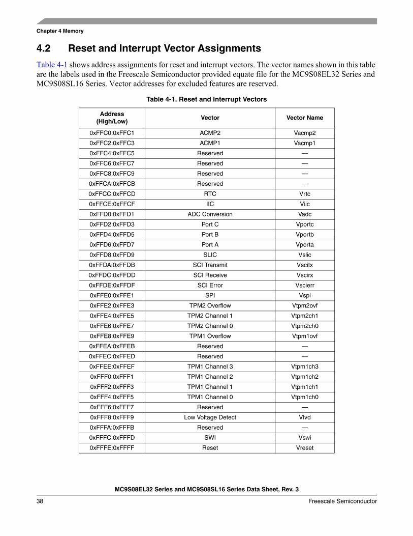
Chapter 4 Memory
MC9S08EL32 Series and MC9S08SL16 Series Data Sheet, Rev. 3
38 Freescale Semiconductor
4.2 Reset and Interrupt Vector Assignments
Table 4-1 shows address assignments for reset and interrupt vectors. The vector names shown in this table are the labels used in the Freescale Semiconductor provided equate file for the MC9S08EL32 Series and MC9S08SL16 Series. Vector addresses for excluded features are reserved.
Table 4-1. Reset and Interrupt Vectors
Address(High/Low)
Vector Vector Name
0xFFC0:0xFFC1 ACMP2 Vacmp2
0xFFC2:0xFFC3 ACMP1 Vacmp1
0xFFC4:0xFFC5 Reserved —
0xFFC6:0xFFC7 Reserved —
0xFFC8:0xFFC9 Reserved —
0xFFCA:0xFFCB Reserved —
0xFFCC:0xFFCD RTC Vrtc
0xFFCE:0xFFCF IIC Viic
0xFFD0:0xFFD1 ADC Conversion Vadc
0xFFD2:0xFFD3 Port C Vportc
0xFFD4:0xFFD5 Port B Vportb
0xFFD6:0xFFD7 Port A Vporta
0xFFD8:0xFFD9 SLIC Vslic
0xFFDA:0xFFDB SCI Transmit Vscitx
0xFFDC:0xFFDD SCI Receive Vscirx
0xFFDE:0xFFDF SCI Error Vscierr
0xFFE0:0xFFE1 SPI Vspi
0xFFE2:0xFFE3 TPM2 Overflow Vtpm2ovf
0xFFE4:0xFFE5 TPM2 Channel 1 Vtpm2ch1
0xFFE6:0xFFE7 TPM2 Channel 0 Vtpm2ch0
0xFFE8:0xFFE9 TPM1 Overflow Vtpm1ovf
0xFFEA:0xFFEB Reserved —
0xFFEC:0xFFED Reserved —
0xFFEE:0xFFEF TPM1 Channel 3 Vtpm1ch3
0xFFF0:0xFFF1 TPM1 Channel 2 Vtpm1ch2
0xFFF2:0xFFF3 TPM1 Channel 1 Vtpm1ch1
0xFFF4:0xFFF5 TPM1 Channel 0 Vtpm1ch0
0xFFF6:0xFFF7 Reserved —
0xFFF8:0xFFF9 Low Voltage Detect Vlvd
0xFFFA:0xFFFB Reserved —
0xFFFC:0xFFFD SWI Vswi
0xFFFE:0xFFFF Reset Vreset
Chapter 4 Memory
MC9S08EL32 Series and MC9S08SL16 Series Data Sheet, Rev. 3
Freescale Semiconductor 39
4.3 Register Addresses and Bit AssignmentsThe registers in the MC9S08EL32 Series and MC9S08SL16 Series are divided into these groups:
• Direct-page registers are located in the first 128 locations in the memory map; these are accessible with efficient direct addressing mode instructions.
• High-page registers are used much less often, so they are located above 0x1800 in the memory map. This leaves more room in the direct page for more frequently used registers and RAM.
• The nonvolatile register area consists of a block of 16 locations in FLASH memory at 0xFFB0–0xFFBF. Nonvolatile register locations include: — NVPROT and NVOPT which are loaded into working registers at reset— An 8-byte backdoor comparison key that optionally allows a user to gain controlled access to
secure memory
Because the nonvolatile register locations are FLASH memory, they must be erased and programmed like other FLASH memory locations.
Direct-page registers can be accessed with efficient direct addressing mode instructions. Bit manipulation instructions can be used to access any bit in any direct-page register. Table 4-2 is a summary of all user-accessible direct-page registers and control bits.
The direct page registers in Table 4-2 can use the more efficient direct addressing mode, which requires only the lower byte of the address. Because of this, the lower byte of the address in column one is shown in bold text. In Table 4-3 and Table 4-4, the whole address in column one is shown in bold. In Table 4-2, Table 4-3, and Table 4-4, the register names in column two are shown in bold to set them apart from the bit names to the right. Cells that are not associated with named bits are shaded. A shaded cell with a 0 indicates this unused bit always reads as a 0. Shaded cells with dashes indicate unused or reserved bit locations that could read as 1s or 0s.
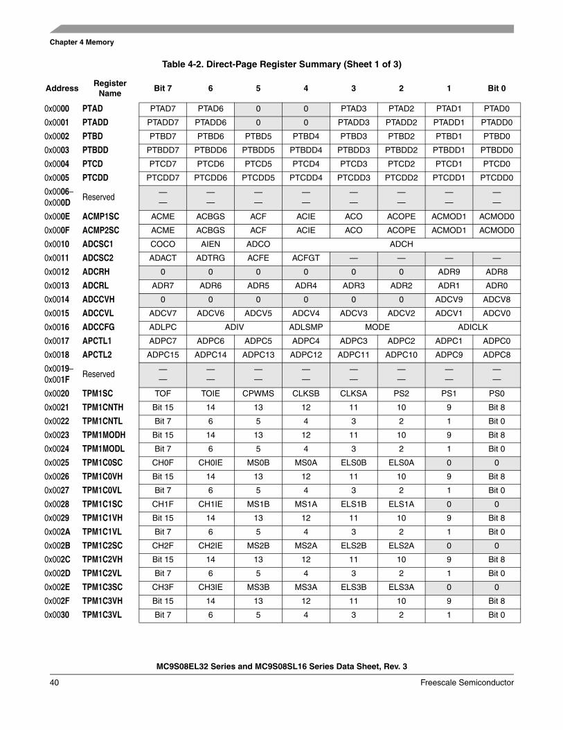
Chapter 4 Memory
MC9S08EL32 Series and MC9S08SL16 Series Data Sheet, Rev. 3
40 Freescale Semiconductor
Table 4-2. Direct-Page Register Summary (Sheet 1 of 3)
AddressRegister
NameBit 7 6 5 4 3 2 1 Bit 0
0x0000 PTAD PTAD7 PTAD6 0 0 PTAD3 PTAD2 PTAD1 PTAD0
0x0001 PTADD PTADD7 PTADD6 0 0 PTADD3 PTADD2 PTADD1 PTADD0
0x0002 PTBD PTBD7 PTBD6 PTBD5 PTBD4 PTBD3 PTBD2 PTBD1 PTBD0
0x0003 PTBDD PTBDD7 PTBDD6 PTBDD5 PTBDD4 PTBDD3 PTBDD2 PTBDD1 PTBDD0
0x0004 PTCD PTCD7 PTCD6 PTCD5 PTCD4 PTCD3 PTCD2 PTCD1 PTCD0
0x0005 PTCDD PTCDD7 PTCDD6 PTCDD5 PTCDD4 PTCDD3 PTCDD2 PTCDD1 PTCDD0
0x0006–0x000D
Reserved ——
——
——
——
——
——
——
——
0x000E ACMP1SC ACME ACBGS ACF ACIE ACO ACOPE ACMOD1 ACMOD0
0x000F ACMP2SC ACME ACBGS ACF ACIE ACO ACOPE ACMOD1 ACMOD0
0x0010 ADCSC1 COCO AIEN ADCO ADCH
0x0011 ADCSC2 ADACT ADTRG ACFE ACFGT — — — —
0x0012 ADCRH 0 0 0 0 0 0 ADR9 ADR8
0x0013 ADCRL ADR7 ADR6 ADR5 ADR4 ADR3 ADR2 ADR1 ADR0
0x0014 ADCCVH 0 0 0 0 0 0 ADCV9 ADCV8
0x0015 ADCCVL ADCV7 ADCV6 ADCV5 ADCV4 ADCV3 ADCV2 ADCV1 ADCV0
0x0016 ADCCFG ADLPC ADIV ADLSMP MODE ADICLK
0x0017 APCTL1 ADPC7 ADPC6 ADPC5 ADPC4 ADPC3 ADPC2 ADPC1 ADPC0
0x0018 APCTL2 ADPC15 ADPC14 ADPC13 ADPC12 ADPC11 ADPC10 ADPC9 ADPC8
0x0019–0x001F
Reserved ——
——
——
——
——
——
——
——
0x0020 TPM1SC TOF TOIE CPWMS CLKSB CLKSA PS2 PS1 PS0
0x0021 TPM1CNTH Bit 15 14 13 12 11 10 9 Bit 8
0x0022 TPM1CNTL Bit 7 6 5 4 3 2 1 Bit 0
0x0023 TPM1MODH Bit 15 14 13 12 11 10 9 Bit 8
0x0024 TPM1MODL Bit 7 6 5 4 3 2 1 Bit 0
0x0025 TPM1C0SC CH0F CH0IE MS0B MS0A ELS0B ELS0A 0 0
0x0026 TPM1C0VH Bit 15 14 13 12 11 10 9 Bit 8
0x0027 TPM1C0VL Bit 7 6 5 4 3 2 1 Bit 0
0x0028 TPM1C1SC CH1F CH1IE MS1B MS1A ELS1B ELS1A 0 0
0x0029 TPM1C1VH Bit 15 14 13 12 11 10 9 Bit 8
0x002A TPM1C1VL Bit 7 6 5 4 3 2 1 Bit 0
0x002B TPM1C2SC CH2F CH2IE MS2B MS2A ELS2B ELS2A 0 0
0x002C TPM1C2VH Bit 15 14 13 12 11 10 9 Bit 8
0x002D TPM1C2VL Bit 7 6 5 4 3 2 1 Bit 0
0x002E TPM1C3SC CH3F CH3IE MS3B MS3A ELS3B ELS3A 0 0
0x002F TPM1C3VH Bit 15 14 13 12 11 10 9 Bit 8
0x0030 TPM1C3VL Bit 7 6 5 4 3 2 1 Bit 0
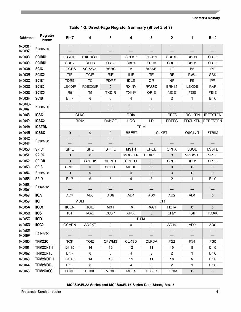
Chapter 4 Memory
MC9S08EL32 Series and MC9S08SL16 Series Data Sheet, Rev. 3
Freescale Semiconductor 41
0x0031–0x0037
Reserved ——
——
——
——
——
——
——
——
0x0038 SCIBDH LBKDIE RXEDGIE 0 SBR12 SBR11 SBR10 SBR9 SBR8
0x0039 SCIBDL SBR7 SBR6 SBR5 SBR4 SBR3 SBR2 SBR1 SBR0
0x003A SCIC1 LOOPS SCISWAI RSRC M WAKE ILT PE PT
0x003B SCIC2 TIE TCIE RIE ILIE TE RE RWU SBK
0x003C SCIS1 TDRE TC RDRF IDLE OR NF FE PF
0x003D SCIS2 LBKDIF RXEDGIF 0 RXINV RWUID BRK13 LBKDE RAF
0x003E SCIC3 R8 T8 TXDIR TXINV ORIE NEIE FEIE PEIE
0x003F SCID Bit 7 6 5 4 3 2 1 Bit 0
0x0040–0x0047
Reserved ——
——
——
——
——
——
——
——
0x0048 ICSC1 CLKS RDIV IREFS IRCLKEN IREFSTEN
0x0049 ICSC2 BDIV RANGE HGO LP EREFS ERCLKEN EREFSTEN
0x004A ICSTRM TRIM
0x004B ICSSC 0 0 0 IREFST CLKST OSCINIT FTRIM
0x004C–0x004F
Reserved ——
——
——
——
——
——
——
——
0x0050 SPIC1 SPIE SPE SPTIE MSTR CPOL CPHA SSOE LSBFE
0x0051 SPIC2 0 0 0 MODFEN BIDIROE 0 SPISWAI SPC0
0x0052 SPIBR 0 SPPR2 SPPR1 SPPR0 0 SPR2 SPR1 SPR0
0x0053 SPIS SPRF 0 SPTEF MODF 0 0 0 0
0x0054 Reserved 0 0 0 0 0 0 0 0
0x0055 SPID Bit 7 6 5 4 3 2 1 Bit 0
0x0056–0x0057
Reserved ——
——
——
——
——
——
——
——
0x0058 IICA AD7 AD6 AD5 AD4 AD3 AD2 AD1 0
0x0059 IICF MULT ICR
0x005A IICC1 IICEN IICIE MST TX TXAK RSTA 0 0
0x005B IICS TCF IAAS BUSY ARBL 0 SRW IICIF RXAK
0x005C IICD DATA
0x005D IICC2 GCAEN ADEXT 0 0 0 AD10 AD9 AD8
0x005E–0x005F
Reserved ——
——
——
——
——
——
——
——
0x0060 TPM2SC TOF TOIE CPWMS CLKSB CLKSA PS2 PS1 PS0
0x0061 TPM2CNTH Bit 15 14 13 12 11 10 9 Bit 8
0x0062 TPM2CNTL Bit 7 6 5 4 3 2 1 Bit 0
0x0063 TPM2MODH Bit 15 14 13 12 11 10 9 Bit 8
0x0064 TPM2MODL Bit 7 6 5 4 3 2 1 Bit 0
0x0065 TPM2C0SC CH0F CH0IE MS0B MS0A ELS0B ELS0A 0 0
Table 4-2. Direct-Page Register Summary (Sheet 2 of 3)
AddressRegister
NameBit 7 6 5 4 3 2 1 Bit 0
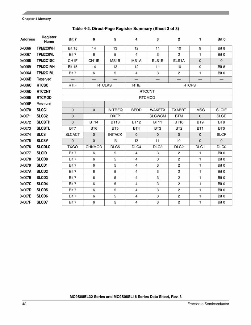
Chapter 4 Memory
MC9S08EL32 Series and MC9S08SL16 Series Data Sheet, Rev. 3
42 Freescale Semiconductor
0x0066 TPM2C0VH Bit 15 14 13 12 11 10 9 Bit 8
0x0067 TPM2C0VL Bit 7 6 5 4 3 2 1 Bit 0
0x0068 TPM2C1SC CH1F CH1IE MS1B MS1A ELS1B ELS1A 0 0
0x0069 TPM2C1VH Bit 15 14 13 12 11 10 9 Bit 8
0x006A TPM2C1VL Bit 7 6 5 4 3 2 1 Bit 0
0x006B Reserved — — — — — — — —
0x006C RTCSC RTIF RTCLKS RTIE RTCPS
0x006D RTCCNT RTCCNT
0x006E RTCMOD RTCMOD
0x006F Reserved — — — — — — — —
0x0070 SLCC1 0 0 INITREQ BEDD WAKETX TXABRT IMSG SLCIE
0x0071 SLCC2 0 RXFP SLCWCM BTM 0 SLCE
0x0072 SLCBTH 0 BT14 BT13 BT12 BT11 BT10 BT9 BT8
0x0073 SLCBTL BT7 BT6 BT5 BT4 BT3 BT2 BT1 BT0
0x0074 SLCS SLCACT 0 INITACK 0 0 0 0 SLCF
0x0075 SLCSV 0 0 I3 I2 I1 I0 0 0
0x0076 SLCDLC TXGO CHKMOD DLC5 DLC4 DLC3 DLC2 DLC1 DLC0
0x0077 SLCID Bit 7 6 5 4 3 2 1 Bit 0
0x0078 SLCD0 Bit 7 6 5 4 3 2 1 Bit 0
0x0079 SLCD1 Bit 7 6 5 4 3 2 1 Bit 0
0x007A SLCD2 Bit 7 6 5 4 3 2 1 Bit 0
0x007B SLCD3 Bit 7 6 5 4 3 2 1 Bit 0
0x007C SLCD4 Bit 7 6 5 4 3 2 1 Bit 0
0x007D SLCD5 Bit 7 6 5 4 3 2 1 Bit 0
0x007E SLCD6 Bit 7 6 5 4 3 2 1 Bit 0
0x007F SLCD7 Bit 7 6 5 4 3 2 1 Bit 0
Table 4-2. Direct-Page Register Summary (Sheet 3 of 3)
AddressRegister
NameBit 7 6 5 4 3 2 1 Bit 0
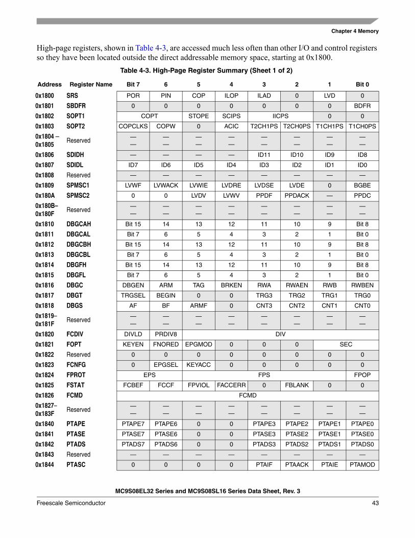
Chapter 4 Memory
MC9S08EL32 Series and MC9S08SL16 Series Data Sheet, Rev. 3
Freescale Semiconductor 43
High-page registers, shown in Table 4-3, are accessed much less often than other I/O and control registers so they have been located outside the direct addressable memory space, starting at 0x1800.
Table 4-3. High-Page Register Summary (Sheet 1 of 2)
Address Register Name Bit 7 6 5 4 3 2 1 Bit 0
0x1800 SRS POR PIN COP ILOP ILAD 0 LVD 0
0x1801 SBDFR 0 0 0 0 0 0 0 BDFR
0x1802 SOPT1 COPT STOPE SCIPS IICPS 0 0
0x1803 SOPT2 COPCLKS COPW 0 ACIC T2CH1PS T2CH0PS T1CH1PS T1CH0PS
0x1804 –0x1805
Reserved ——
——
——
——
——
——
——
——
0x1806 SDIDH — — — — ID11 ID10 ID9 ID8
0x1807 SDIDL ID7 ID6 ID5 ID4 ID3 ID2 ID1 ID0
0x1808 Reserved — — — — — — — —
0x1809 SPMSC1 LVWF LVWACK LVWIE LVDRE LVDSE LVDE 0 BGBE
0x180A SPMSC2 0 0 LVDV LVWV PPDF PPDACK — PPDC
0x180B–0x180F
Reserved ——
——
——
——
——
——
——
——
0x1810 DBGCAH Bit 15 14 13 12 11 10 9 Bit 8
0x1811 DBGCAL Bit 7 6 5 4 3 2 1 Bit 0
0x1812 DBGCBH Bit 15 14 13 12 11 10 9 Bit 8
0x1813 DBGCBL Bit 7 6 5 4 3 2 1 Bit 0
0x1814 DBGFH Bit 15 14 13 12 11 10 9 Bit 8
0x1815 DBGFL Bit 7 6 5 4 3 2 1 Bit 0
0x1816 DBGC DBGEN ARM TAG BRKEN RWA RWAEN RWB RWBEN
0x1817 DBGT TRGSEL BEGIN 0 0 TRG3 TRG2 TRG1 TRG0
0x1818 DBGS AF BF ARMF 0 CNT3 CNT2 CNT1 CNT0
0x1819–0x181F
Reserved ——
——
——
——
——
——
——
——
0x1820 FCDIV DIVLD PRDIV8 DIV
0x1821 FOPT KEYEN FNORED EPGMOD 0 0 0 SEC
0x1822 Reserved 0 0 0 0 0 0 0 0
0x1823 FCNFG 0 EPGSEL KEYACC 0 0 0 0 0
0x1824 FPROT EPS FPS FPOP
0x1825 FSTAT FCBEF FCCF FPVIOL FACCERR 0 FBLANK 0 0
0x1826 FCMD FCMD
0x1827–0x183F
Reserved ——
——
——
——
——
——
——
——
0x1840 PTAPE PTAPE7 PTAPE6 0 0 PTAPE3 PTAPE2 PTAPE1 PTAPE0
0x1841 PTASE PTASE7 PTASE6 0 0 PTASE3 PTASE2 PTASE1 PTASE0
0x1842 PTADS PTADS7 PTADS6 0 0 PTADS3 PTADS2 PTADS1 PTADS0
0x1843 Reserved — — — — — — — —
0x1844 PTASC 0 0 0 0 PTAIF PTAACK PTAIE PTAMOD
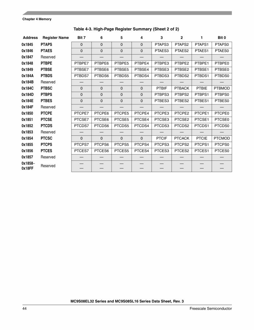
Chapter 4 Memory
MC9S08EL32 Series and MC9S08SL16 Series Data Sheet, Rev. 3
44 Freescale Semiconductor
0x1845 PTAPS 0 0 0 0 PTAPS3 PTAPS2 PTAPS1 PTAPS0
0x1846 PTAES 0 0 0 0 PTAES3 PTAES2 PTAES1 PTAES0
0x1847 Reserved — — — — — — — —
0x1848 PTBPE PTBPE7 PTBPE6 PTBPE5 PTBPE4 PTBPE3 PTBPE2 PTBPE1 PTBPE0
0x1849 PTBSE PTBSE7 PTBSE6 PTBSE5 PTBSE4 PTBSE3 PTBSE2 PTBSE1 PTBSE0
0x184A PTBDS PTBDS7 PTBDS6 PTBDS5 PTBDS4 PTBDS3 PTBDS2 PTBDS1 PTBDS0
0x184B Reserved — — — — — — — —
0x184C PTBSC 0 0 0 0 PTBIF PTBACK PTBIE PTBMOD
0x184D PTBPS 0 0 0 0 PTBPS3 PTBPS2 PTBPS1 PTBPS0
0x184E PTBES 0 0 0 0 PTBES3 PTBES2 PTBES1 PTBES0
0x184F Reserved — — — — — — — —
0x1850 PTCPE PTCPE7 PTCPE6 PTCPE5 PTCPE4 PTCPE3 PTCPE2 PTCPE1 PTCPE0
0x1851 PTCSE PTCSE7 PTCSE6 PTCSE5 PTCSE4 PTCSE3 PTCSE2 PTCSE1 PTCSE0
0x1852 PTCDS PTCDS7 PTCDS6 PTCDS5 PTCDS4 PTCDS3 PTCDS2 PTCDS1 PTCDS0
0x1853 Reserved — — — — — — — —
0x1854 PTCSC 0 0 0 0 PTCIF PTCACK PTCIE PTCMOD
0x1855 PTCPS PTCPS7 PTCPS6 PTCPS5 PTCPS4 PTCPS3 PTCPS2 PTCPS1 PTCPS0
0x1856 PTCES PTCES7 PTCES6 PTCES5 PTCES4 PTCES3 PTCES2 PTCES1 PTCES0
0x1857 Reserved — — — — — — — —
0x1858–0x18FF
Reserved ——
——
——
——
——
——
——
——
Table 4-3. High-Page Register Summary (Sheet 2 of 2)
Address Register Name Bit 7 6 5 4 3 2 1 Bit 0
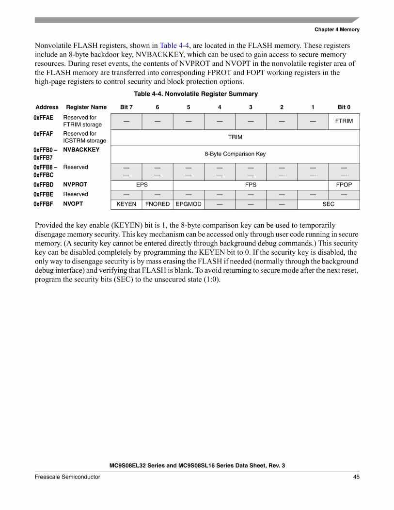
Chapter 4 Memory
MC9S08EL32 Series and MC9S08SL16 Series Data Sheet, Rev. 3
Freescale Semiconductor 45
Nonvolatile FLASH registers, shown in Table 4-4, are located in the FLASH memory. These registers include an 8-byte backdoor key, NVBACKKEY, which can be used to gain access to secure memory resources. During reset events, the contents of NVPROT and NVOPT in the nonvolatile register area of the FLASH memory are transferred into corresponding FPROT and FOPT working registers in the high-page registers to control security and block protection options.
Provided the key enable (KEYEN) bit is 1, the 8-byte comparison key can be used to temporarily disengage memory security. This key mechanism can be accessed only through user code running in secure memory. (A security key cannot be entered directly through background debug commands.) This security key can be disabled completely by programming the KEYEN bit to 0. If the security key is disabled, the only way to disengage security is by mass erasing the FLASH if needed (normally through the background debug interface) and verifying that FLASH is blank. To avoid returning to secure mode after the next reset, program the security bits (SEC) to the unsecured state (1:0).
Table 4-4. Nonvolatile Register Summary
Address Register Name Bit 7 6 5 4 3 2 1 Bit 0
0xFFAE Reserved for FTRIM storage
— — — — — — — FTRIM
0xFFAF Reserved for ICSTRM storage
TRIM
0xFFB0 –0xFFB7
NVBACKKEY8-Byte Comparison Key
0xFFB8 –0xFFBC
Reserved ——
——
——
——
——
——
——
——
0xFFBD NVPROT EPS FPS FPOP
0xFFBE Reserved — — — — — — — —
0xFFBF NVOPT KEYEN FNORED EPGMOD — — — SEC
Chapter 4 Memory
MC9S08EL32 Series and MC9S08SL16 Series Data Sheet, Rev. 3
46 Freescale Semiconductor
4.4 RAMThe MC9S08EL32 Series and MC9S08SL16 Series includes static RAM. The locations in RAM below 0x0100 can be accessed using the more efficient direct addressing mode, and any single bit in this area can be accessed with the bit manipulation instructions (BCLR, BSET, BRCLR, and BRSET). Locating the most frequently accessed program variables in this area of RAM is preferred.
The RAM retains data when the MCU is in low-power wait, stop2, or stop3 mode. At power-on the contents of RAM are uninitialized. RAM data is unaffected by any reset provided that the supply voltage does not drop below the minimum value for RAM retention (VRAM).
For compatibility with M68HC05 MCUs, the HCS08 resets the stack pointer to 0x00FF. In the MC9S08EL32 Series and MC9S08SL16 Series, it is usually best to reinitialize the stack pointer to the top of the RAM so the direct page RAM can be used for frequently accessed RAM variables and bit-addressable program variables. Include the following 2-instruction sequence in your reset initialization routine (where RamLast is equated to the highest address of the RAM in the Freescale Semiconductor-provided equate file). LDHX #RamLast+1 ;point one past RAM TXS ;SP<-(H:X-1)
When security is enabled, the RAM is considered a secure memory resource and is not accessible through BDM or through code executing from non-secure memory. See Section 4.5.9, “Security”, for a detailed description of the security feature.
Chapter 4 Memory
MC9S08EL32 Series and MC9S08SL16 Series Data Sheet, Rev. 3
Freescale Semiconductor 47
4.5 FLASH and EEPROMThe MC9S08EL32 Series and MC9S08SL16 Series includes FLASH and EEPROM memory intended primarily for program and data storage. In-circuit programming allows the operating program and data to be loaded into FLASH and EEPROM, respectively, after final assembly of the application product. It is possible to program the arrays through the single-wire background debug interface. Because no special voltages are needed for erase and programming operations, in-application programming is also possible through other software-controlled communication paths. For a more detailed discussion of in-circuit and in-application programming, refer to the HCS08 Family Reference Manual, Volume I, Freescale Semiconductor document order number HCS08RMv1/D.
4.5.1 Features
Features of the FLASH and EEPROM memory include:• Array size
— MC9S08EL32: 32,768 bytes of FLASH, 512 bytes of EEPROM— MC9S08EL16: 16,384 bytes of FLASH, 512 bytes of EEPROM— MC9S08SL16: 16,384 bytes of FLASH, 256 bytes of EEPROM— MC9S08SL8: 8,192 bytes of FLASH, 256 bytes of EEPROM
• Sector size: 512 bytes for FLASH, 8 bytes for EEPROM• Single power supply program and erase• Command interface for fast program and erase operation• Up to 100,000 program/erase cycles at typical voltage and temperature• Flexible block protection and vector redirection• Security feature for FLASH, EEPROM, and RAM
4.5.2 Program and Erase Times
Before any program or erase command can be accepted, the FLASH and EEPROM clock divider register (FCDIV) must be written to set the internal clock for the FLASH and EEPROM module to a frequency (fFCLK) between 150 kHz and 200 kHz (see Section 4.5.11.1, “FLASH and EEPROM Clock Divider Register (FCDIV)”). This register can be written only once, so normally this write is performed during reset initialization. FCDIV cannot be written if the access error flag, FACCERR in FSTAT, is set. The user must ensure that FACCERR is not set before writing to the FCDIV register. One period of the resulting clock (1/fFCLK) is used by the command processor to time program and erase pulses. An integer number of these timing pulses is used by the command processor to complete a program or erase command.
Table 4-5 shows program and erase times. The bus clock frequency and FCDIV determine the frequency of FCLK (fFCLK). The time for one cycle of FCLK is tFCLK = 1/fFCLK. The times are shown as a number of cycles of FCLK and as an absolute time for the case where tFCLK = 5 μs. Program and erase times shown include overhead for the command state machine and enabling and disabling of program and erase voltages.
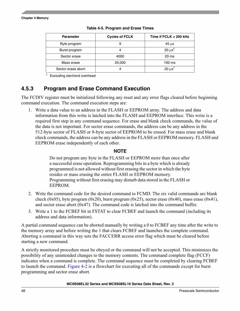
Chapter 4 Memory
MC9S08EL32 Series and MC9S08SL16 Series Data Sheet, Rev. 3
48 Freescale Semiconductor
4.5.3 Program and Erase Command Execution
The FCDIV register must be initialized following any reset and any error flags cleared before beginning command execution. The command execution steps are:
1. Write a data value to an address in the FLASH or EEPROM array. The address and data information from this write is latched into the FLASH and EEPROM interface. This write is a required first step in any command sequence. For erase and blank check commands, the value of the data is not important. For sector erase commands, the address can be any address in the 512-byte sector of FLASH or 8-byte sector of EEPROM to be erased. For mass erase and blank check commands, the address can be any address in the FLASH or EEPROM memory. FLASH and EEPROM erase independently of each other.
NOTEDo not program any byte in the FLASH or EEPROM more than once after a successful erase operation. Reprogramming bits in a byte which is already programmed is not allowed without first erasing the sector in which the byte resides or mass erasing the entire FLASH or EEPROM memory. Programming without first erasing may disturb data stored in the FLASH or EEPROM.
2. Write the command code for the desired command to FCMD. The six valid commands are blank check (0x05), byte program (0x20), burst program (0x25), sector erase (0x40), mass erase (0x41), and sector erase abort (0x47). The command code is latched into the command buffer.
3. Write a 1 to the FCBEF bit in FSTAT to clear FCBEF and launch the command (including its address and data information).
A partial command sequence can be aborted manually by writing a 0 to FCBEF any time after the write to the memory array and before writing the 1 that clears FCBEF and launches the complete command. Aborting a command in this way sets the FACCERR access error flag which must be cleared before starting a new command.
A strictly monitored procedure must be obeyed or the command will not be accepted. This minimizes the possibility of any unintended changes to the memory contents. The command complete flag (FCCF) indicates when a command is complete. The command sequence must be completed by clearing FCBEF to launch the command. Figure 4-2 is a flowchart for executing all of the commands except for burst programming and sector erase abort.
Table 4-5. Program and Erase Times
Parameter Cycles of FCLK Time if FCLK = 200 kHz
Byte program 9 45 μs
Burst program 4 20 μs1
1 Excluding start/end overhead
Sector erase 4000 20 ms
Mass erase 20,000 100 ms
Sector erase abort 4 20 μs1
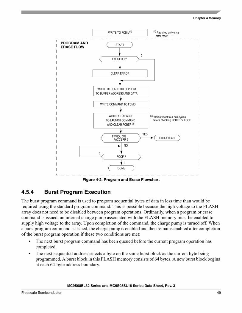
Chapter 4 Memory
MC9S08EL32 Series and MC9S08SL16 Series Data Sheet, Rev. 3
Freescale Semiconductor 49
Figure 4-2. Program and Erase Flowchart
4.5.4 Burst Program Execution
The burst program command is used to program sequential bytes of data in less time than would be required using the standard program command. This is possible because the high voltage to the FLASH array does not need to be disabled between program operations. Ordinarily, when a program or erase command is issued, an internal charge pump associated with the FLASH memory must be enabled to supply high voltage to the array. Upon completion of the command, the charge pump is turned off. When a burst program command is issued, the charge pump is enabled and then remains enabled after completion of the burst program operation if these two conditions are met:
• The next burst program command has been queued before the current program operation has completed.
• The next sequential address selects a byte on the same burst block as the current byte being programmed. A burst block in this FLASH memory consists of 64 bytes. A new burst block begins at each 64-byte address boundary.
START
WRITE TO FLASH OR EEPROMTO BUFFER ADDRESS AND DATA
WRITE COMMAND TO FCMD
NO
YESFPVIOL OR
WRITE 1 TO FCBEFTO LAUNCH COMMAND AND CLEAR FCBEF (2)
1
0FCCF ?
ERROR EXIT
DONE
(2) Wait at least four bus cyclesbefore checking FCBEF or FCCF.
0FACCERR ?
CLEAR ERROR
FACCERR ?
WRITE TO FCDIV(1) (1) Required only onceafter reset.
PROGRAM ANDERASE FLOW
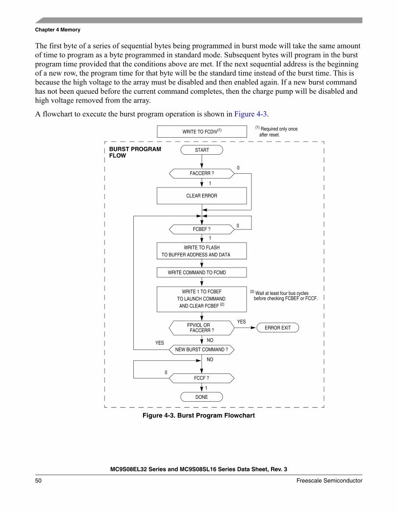
Chapter 4 Memory
MC9S08EL32 Series and MC9S08SL16 Series Data Sheet, Rev. 3
50 Freescale Semiconductor
The first byte of a series of sequential bytes being programmed in burst mode will take the same amount of time to program as a byte programmed in standard mode. Subsequent bytes will program in the burst program time provided that the conditions above are met. If the next sequential address is the beginning of a new row, the program time for that byte will be the standard time instead of the burst time. This is because the high voltage to the array must be disabled and then enabled again. If a new burst command has not been queued before the current command completes, then the charge pump will be disabled and high voltage removed from the array.
A flowchart to execute the burst program operation is shown in Figure 4-3.
Figure 4-3. Burst Program Flowchart
1
0FCBEF ?
START
WRITE TO FLASHTO BUFFER ADDRESS AND DATA
WRITE COMMAND TO FCMD
NO
YESFPVIOL OR
WRITE 1 TO FCBEFTO LAUNCH COMMAND AND CLEAR FCBEF (2)
NO
YESNEW BURST COMMAND ?
1
0FCCF ?
ERROR EXIT
DONE
(2) Wait at least four bus cycles before checking FCBEF or FCCF.
1
0FACCERR ?
CLEAR ERROR
FACCERR ?
WRITE TO FCDIV(1)(1) Required only once
after reset.
BURST PROGRAMFLOW
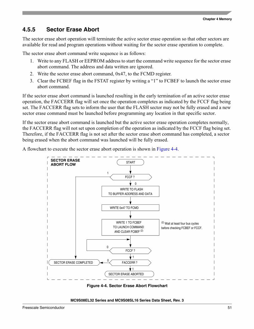
Chapter 4 Memory
MC9S08EL32 Series and MC9S08SL16 Series Data Sheet, Rev. 3
Freescale Semiconductor 51
4.5.5 Sector Erase Abort
The sector erase abort operation will terminate the active sector erase operation so that other sectors are available for read and program operations without waiting for the sector erase operation to complete.
The sector erase abort command write sequence is as follows:1. Write to any FLASH or EEPROM address to start the command write sequence for the sector erase
abort command. The address and data written are ignored.2. Write the sector erase abort command, 0x47, to the FCMD register.3. Clear the FCBEF flag in the FSTAT register by writing a “1” to FCBEF to launch the sector erase
abort command.
If the sector erase abort command is launched resulting in the early termination of an active sector erase operation, the FACCERR flag will set once the operation completes as indicated by the FCCF flag being set. The FACCERR flag sets to inform the user that the FLASH sector may not be fully erased and a new sector erase command must be launched before programming any location in that specific sector.
If the sector erase abort command is launched but the active sector erase operation completes normally, the FACCERR flag will not set upon completion of the operation as indicated by the FCCF flag being set. Therefore, if the FACCERR flag is not set after the sector erase abort command has completed, a sector being erased when the abort command was launched will be fully erased.
A flowchart to execute the sector erase abort operation is shown in Figure 4-4.
Figure 4-4. Sector Erase Abort Flowchart
START
WRITE 0x47 TO FCMD
WRITE 1 TO FCBEFTO LAUNCH COMMAND AND CLEAR FCBEF (2)
1
0FCCF ?
SECTOR ERASE ABORTED
(2) Wait at least four bus cycles
0
1FCCF ?
WRITE TO FLASHTO BUFFER ADDRESS AND DATA
FACCERR ?0
1
SECTOR ERASE COMPLETED
before checking FCBEF or FCCF.
SECTOR ERASEABORT FLOW
Chapter 4 Memory
MC9S08EL32 Series and MC9S08SL16 Series Data Sheet, Rev. 3
52 Freescale Semiconductor
NOTEThe FCBEF flag will not set after launching the sector erase abort command. If an attempt is made to start a new command write sequence with a sector erase abort operation active, the FACCERR flag in the FSTAT register will be set. A new command write sequence may be started after clearing the ACCERR flag, if set.
NOTEThe sector erase abort command should be used sparingly since a sector erase operation that is aborted counts as a complete program/erase cycle.
4.5.6 Access Errors
An access error occurs whenever the command execution protocol is violated.
Any of the following specific actions will cause the access error flag (FACCERR) in FSTAT to be set. FACCERR must be cleared by writing a 1 to FACCERR in FSTAT before any command can be processed.
• Writing to a FLASH address before the internal FLASH and EEPROM clock frequency has been set by writing to the FCDIV register.
• Writing to a FLASH address while FCBEF is not set. (A new command cannot be started until the command buffer is empty.)
• Writing a second time to a FLASH address before launching the previous command. (There is only one write to FLASH for every command.)
• Writing a second time to FCMD before launching the previous command. (There is only one write to FCMD for every command.)
• Writing to any FLASH control register other than FCMD after writing to a FLASH address.• Writing any command code other than the six allowed codes (0x05, 0x20, 0x25, 0x40, 0x41, or
0x47) to FCMD.• Writing any FLASH control register other than to write to FSTAT (to clear FCBEF and launch the
command) after writing the command to FCMD.• The MCU enters stop mode while a program or erase command is in progress. (The command is
aborted.)• Writing the byte program, burst program, sector erase or sector erase abort command code (0x20,
0x25, 0x40, or 0x47) with a background debug command while the MCU is secured. (The background debug controller can do blank check and mass erase commands only when the MCU is secure.)
• Writing 0 to FCBEF to cancel a partial command.
Chapter 4 Memory
MC9S08EL32 Series and MC9S08SL16 Series Data Sheet, Rev. 3
Freescale Semiconductor 53
4.5.7 Block Protection
The block protection feature prevents the protected region of FLASH or EEPROM from program or erase changes. Block protection is controlled through the FLASH and EEPROM protection register (FPROT). The EPS bits determine the protected region of EEPROM and the FPS bits determine the protected region of FLASH. See Section 4.5.11.4, “FLASH and EEPROM Protection Register (FPROT and NVPROT)”.
After exit from reset, FPROT is loaded with the contents of the NVPROT location, which is in the nonvolatile register block of the FLASH memory. FPROT cannot be changed directly from application software so a runaway program cannot alter the block protection settings. Because NVPROT is within the last sector of FLASH, if any amount of memory is protected, NVPROT is itself protected and cannot be altered (intentionally or unintentionally) by the application software. FPROT can be written through background debug commands, which provides a way to erase and reprogram protected FLASH memory.
One use for block protection is to block protect an area of FLASH memory for a bootloader program. This bootloader program can call a routine outside of FLASH that can sector erase the rest of the FLASH memory and reprogram it. The bootloader is protected even if MCU power is lost during an erase and reprogram operation.
4.5.8 Vector Redirection
Whenever any FLASH is block protected, the reset and interrupt vectors will be protected. Vector redirection allows users to modify interrupt vector information without unprotecting bootloader and reset vector space. Vector redirection is enabled by programming the FNORED bit in the NVOPT register located at address 0xFFBF to 0. For redirection to occur, at least some portion of the FLASH memory must be block protected by programming the NVPROT register located at address 0xFFBD. All interrupt vectors (memory locations 0xFFC0–0xFFFD) are redirected, though the reset vector (0xFFFE:0xFFFF) is not.
For example, if 1024 bytes of FLASH are protected, the protected address region is from 0xFC00 through 0xFFFF. The interrupt vectors (0xFFC0–0xFFFD) are redirected to the locations 0xFBC0–0xFBFD. If vector redirection is enabled and an interrupt occurs, the values in the locations 0xFBE0:0xFBE1 are used for the vector instead of the values in the locations 0xFFE0:0xFFE1. This allows the user to reprogram the unprotected portion of the FLASH with new program code including new interrupt vector values while leaving the protected area, which includes the default vector locations, unchanged.
4.5.9 Security
The MC9S08EL32 Series and MC9S08SL16 Series includes circuitry to prevent unauthorized access to the contents of FLASH, EEPROM, and RAM memory. When security is engaged, FLASH, EEPROM, and RAM are considered secure resources. Direct-page registers, high-page registers, and the background debug controller are considered unsecured resources. Programs executing within secure memory have normal access to any MCU memory locations and resources. Attempts to access a secure memory location with a program executing from an unsecured memory space or through the background debug interface are blocked (writes are ignored and reads return all 0s).
Security is engaged or disengaged based on the state of two register bits (SEC[1:0]) in the FOPT register. During reset, the contents of the nonvolatile location NVOPT are copied from FLASH into the working
Chapter 4 Memory
MC9S08EL32 Series and MC9S08SL16 Series Data Sheet, Rev. 3
54 Freescale Semiconductor
FOPT register in high-page register space. A user engages security by programming the NVOPT location, which can be performed at the same time the FLASH memory is programmed. The 1:0 state disengages security; the other three combinations engage security. Notice the erased state (1:1) makes the MCU secure. During development, whenever the FLASH is erased, it is good practice to immediately program the SEC0 bit to 0 in NVOPT so SEC = 1:0. This would allow the MCU to remain unsecured after a subsequent reset.
The on-chip debug module cannot be enabled while the MCU is secure. The separate background debug controller can be used for background memory access commands of unsecured resources.
A user can choose to allow or disallow a security unlocking mechanism through an 8-byte backdoor security key. If the nonvolatile KEYEN bit in NVOPT/FOPT is 0, the backdoor key is disabled and there is no way to disengage security without completely erasing all FLASH locations. If KEYEN is 1, a secure user program can temporarily disengage security by:
1. Writing 1 to KEYACC in the FCNFG register. This makes the FLASH module interpret writes to the backdoor comparison key locations (NVBACKKEY through NVBACKKEY+7) as values to be compared against the key rather than as the first step in a FLASH program or erase command.
2. Writing the user-entered key values to the NVBACKKEY through NVBACKKEY+7 locations. These writes must be performed in order starting with the value for NVBACKKEY and ending with NVBACKKEY+7. STHX must not be used for these writes because these writes cannot be performed on adjacent bus cycles. User software normally would get the key codes from outside the MCU system through a communication interface such as a serial I/O.
3. Writing 0 to KEYACC in the FCNFG register. If the 8-byte key that was written matches the key stored in the FLASH locations, SEC bits are automatically changed to 1:0 and security will be disengaged until the next reset.
The security key can be written only from secure memory (either RAM, EEPROM, or FLASH), so it cannot be entered through background commands without the cooperation of a secure user program.
The backdoor comparison key (NVBACKKEY through NVBACKKEY+7) is located in FLASH memory locations in the nonvolatile register space so users can program these locations exactly as they would program any other FLASH memory location. The nonvolatile registers are in the same 768-byte block of FLASH as the reset and interrupt vectors, so block protecting that space also block protects the backdoor comparison key. Block protects cannot be changed from user application programs, so if the vector space is block protected, the backdoor security key mechanism cannot permanently change the block protect, security settings, or the backdoor key.
Security can always be disengaged through the background debug interface by taking these steps:1. Disable any block protections by writing FPROT. FPROT can be written only with background
debug commands, not from application software.2. Mass erase FLASH if necessary.3. Blank check FLASH. Provided FLASH is completely erased, security is disengaged until the next
reset.
To avoid returning to secure mode after the next reset, program NVOPT so SEC = 1:0.
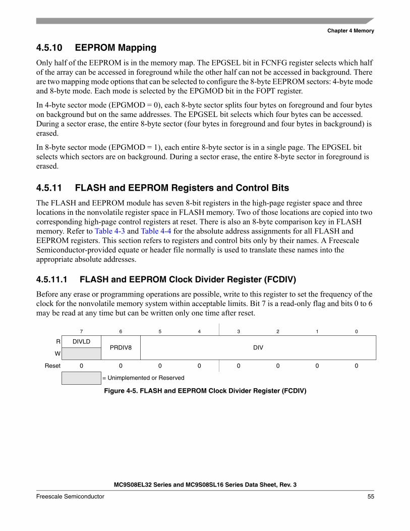
Chapter 4 Memory
MC9S08EL32 Series and MC9S08SL16 Series Data Sheet, Rev. 3
Freescale Semiconductor 55
4.5.10 EEPROM Mapping
Only half of the EEPROM is in the memory map. The EPGSEL bit in FCNFG register selects which half of the array can be accessed in foreground while the other half can not be accessed in background. There are two mapping mode options that can be selected to configure the 8-byte EEPROM sectors: 4-byte mode and 8-byte mode. Each mode is selected by the EPGMOD bit in the FOPT register.
In 4-byte sector mode (EPGMOD = 0), each 8-byte sector splits four bytes on foreground and four bytes on background but on the same addresses. The EPGSEL bit selects which four bytes can be accessed. During a sector erase, the entire 8-byte sector (four bytes in foreground and four bytes in background) is erased.
In 8-byte sector mode (EPGMOD = 1), each entire 8-byte sector is in a single page. The EPGSEL bit selects which sectors are on background. During a sector erase, the entire 8-byte sector in foreground is erased.
4.5.11 FLASH and EEPROM Registers and Control Bits
The FLASH and EEPROM module has seven 8-bit registers in the high-page register space and three locations in the nonvolatile register space in FLASH memory. Two of those locations are copied into two corresponding high-page control registers at reset. There is also an 8-byte comparison key in FLASH memory. Refer to Table 4-3 and Table 4-4 for the absolute address assignments for all FLASH and EEPROM registers. This section refers to registers and control bits only by their names. A Freescale Semiconductor-provided equate or header file normally is used to translate these names into the appropriate absolute addresses.
4.5.11.1 FLASH and EEPROM Clock Divider Register (FCDIV)
Before any erase or programming operations are possible, write to this register to set the frequency of the clock for the nonvolatile memory system within acceptable limits. Bit 7 is a read-only flag and bits 0 to 6 may be read at any time but can be written only one time after reset.
7 6 5 4 3 2 1 0
R DIVLDPRDIV8 DIV
W
Reset 0 0 0 0 0 0 0 0
= Unimplemented or Reserved
Figure 4-5. FLASH and EEPROM Clock Divider Register (FCDIV)
Chapter 4 Memory
MC9S08EL32 Series and MC9S08SL16 Series Data Sheet, Rev. 3
56 Freescale Semiconductor
if PRDIV8 = 0 — fFCLK = fBus ÷ (DIV + 1) Eqn. 4-1
if PRDIV8 = 1 — fFCLK = fBus ÷ (8 × (DIV + 1)) Eqn. 4-2
Table 4-7 shows the appropriate values for PRDIV8 and DIV for selected bus frequencies.
Table 4-6. FCDIV Register Field Descriptions
Field Description
7DIVLD
Divisor Loaded Status Flag — When set, this read-only status flag indicates that the FCDIV register has been written since reset. Reset clears this bit and the first write to this register causes this bit to become set regardless of the data written.0 FCDIV has not been written since reset; erase and program operations disabled for FLASH and EEPROM.1 FCDIV has been written since reset; erase and program operations enabled for FLASH and EEPROM.
6PRDIV8
Prescale (Divide) FLASH and EEPROM Clock by 8 0 Clock input to the FLASH and EEPROM clock divider is the bus rate clock.1 Clock input to the FLASH and EEPROM clock divider is the bus rate clock divided by 8.
5:0DIV
Divisor for FLASH and EEPROM Clock Divider — The FLASH and EEPROM clock divider divides the bus rate clock (or the bus rate clock divided by 8 if PRDIV8 = 1) by the value in the 6-bit DIV field plus one. The resulting frequency of the internal FLASH and EEPROM clock must fall within the range of 200 kHz to 150 kHz for proper FLASH operations. Program/Erase timing pulses are one cycle of this internal FLASH and EEPROM clock which corresponds to a range of 5 μs to 6.7 μs. The automated programming logic uses an integer number of these pulses to complete an erase or program operation. See Equation 4-1 and Equation 4-2.
Table 4-7. FLASH and EEPROM clock divider Settings
fBusPRDIV8(Binary)
DIV(Decimal)
fFCLKProgram/Erase Timing Pulse
(5 μs Min, 6.7 μs Max)
20 MHz 1 12 192.3 kHz 5.2 μs
10 MHz 0 49 200 kHz 5 μs
8 MHz 0 39 200 kHz 5 μs
4 MHz 0 19 200 kHz 5 μs
2 MHz 0 9 200 kHz 5 μs
1 MHz 0 4 200 kHz 5 μs
200 kHz 0 0 200 kHz 5 μs
150 kHz 0 0 150 kHz 6.7 μs
Chapter 4 Memory
MC9S08EL32 Series and MC9S08SL16 Series Data Sheet, Rev. 3
Freescale Semiconductor 57
4.5.11.2 FLASH and EEPROM Options Register (FOPT and NVOPT)
During reset, the contents of the nonvolatile location NVOPT are copied from FLASH into FOPT. To change the value in this register, erase and reprogram the NVOPT location in FLASH memory as usual and then issue a new MCU reset.
7 6 5 4 3 2 1 0
R KEYEN FNORED EPGMOD 0 0 0 SEC
W
Reset F F F 0 0 0 F F
= Unimplemented or Reserved
Figure 4-6. FLASH and EEPROM Options Register (FOPT)
Table 4-8. FOPT Register Field Descriptions
Field Description
7KEYEN
Backdoor Key Mechanism Enable — When this bit is 0, the backdoor key mechanism cannot be used to disengage security. The backdoor key mechanism is accessible only from user (secured) firmware. BDM commands cannot be used to write key comparison values that would unlock the backdoor key. For more detailed information about the backdoor key mechanism, refer to Section 4.5.9, “Security.”0 No backdoor key access allowed.1 If user firmware writes an 8-byte value that matches the nonvolatile backdoor key (NVBACKKEY through
NVBACKKEY+7 in that order), security is temporarily disengaged until the next MCU reset.
6FNORED
Vector Redirection Disable — When this bit is 1, then vector redirection is disabled.0 Vector redirection enabled.1 Vector redirection disabled.
5EPGMOD
EEPROM Sector Mode — When this bit is 0, each sector is split into two pages (4-byte mode). When this bit is 1, each sector is in a single page (8-byte mode).0 Half of each EEPROM sector is in Page 0 and the other half is in Page 1.1 Each sector is in a single page.
1:0SEC
Security State Code — This 2-bit field determines the security state of the MCU as shown in Table 4-9. When the MCU is secure, the contents of RAM, EEPROM and FLASH memory cannot be accessed by instructions from any unsecured source including the background debug interface. SEC changes to 1:0 after successful backdoor key entry or a successful blank check of FLASH. For more detailed information about security, refer to Section 4.5.9, “Security.”
Table 4-9. Security States1
1 SEC changes to 1:0 after successful backdoor key entry or a successful blank check of FLASH.
SEC[1:0] Description
0:0 secure
0:1 secure
1:0 unsecured
1:1 secure
Chapter 4 Memory
MC9S08EL32 Series and MC9S08SL16 Series Data Sheet, Rev. 3
58 Freescale Semiconductor
4.5.11.3 FLASH and EEPROM Configuration Register (FCNFG)
7 6 5 4 3 2 1 0
R 0EPGSEL KEYACC
0 0 0 0 0
W
Reset 0 0 0 0 0 0 0 0
= Unimplemented or Reserved
Figure 4-7. FLASH and EEPROM Configuration Register (FCNFG)
Table 4-10. FCNFG Register Field Descriptions
Field Description
6EPGSEL
EEPROM Page Select — This bit selects which EEPROM page is accessed in the memory map.0 Page 0 is in foreground of memory map. Page 1 is in background and can not be accessed.1 Page 1 is in foreground of memory map. Page 0 is in background and can not be accessed.
5KEYACC
Enable Writing of Access Key — This bit enables writing of the backdoor comparison key. For more detailed information about the backdoor key mechanism, refer to Section 4.5.9, “Security.”0 Writes to 0xFFB0–0xFFB7 are interpreted as the start of a FLASH programming or erase command.1 Writes to NVBACKKEY (0xFFB0–0xFFB7) are interpreted as comparison key writes.
Chapter 4 Memory
MC9S08EL32 Series and MC9S08SL16 Series Data Sheet, Rev. 3
Freescale Semiconductor 59
4.5.11.4 FLASH and EEPROM Protection Register (FPROT and NVPROT)
FPROT register defines which FLASH and EEPROM sectors are protected against program and erase operations.
During the reset sequence, the FPROT register is loaded from the nonvolatile location NVPROT. To change the protection that will be loaded during the reset sequence, the sector containing NVPROT must be unprotected and erased, then NVPROT can be reprogrammed.
FPROT bits are readable at any time and writable as long as the size of the protected region is being increased. Any write to FPROT that attempts to decrease the size of the protected region will be ignored.
Trying to alter data in any protected area will result in a protection violation error and the FPVIOL flag will be set in the FSTAT register. Mass erase is not possible if any one of the sectors is protected.
Figure 4-8. FLASH and EEPROM Protection Register (FPROT)
7 6 5 4 3 2 1 0
REPS FPS FPOP
W
Reset F F F F F F F F
Table 4-11. FPROT Register Field Descriptions
Field Description
7:6EPS
EEPROM Protect Select Bits — This 2-bit field determines the protected EEPROM locations that cannot be erased or programmed. See Table 4-12.
5:1FPS
FLASH Protect Select Bits — This 5-bit field determines the protected FLASH locations that cannot be erased or programmed. See Table 4-13.
0FPOP
FLASH Protect Open Bit — This bit determines the protected FLASH locations that cannot be erased or programmed. See Table 4-13.
Table 4-12. EEPROM Block Protection
EPSAddress Area
ProtectedMemory Size
Protected (bytes)Number of Sectors
Protected
0x3 N/A 0 0
0x2 0x17F8 - 0x17FF 16 2
0x1 0x17F0 - 0x17FF 32 4
0x0 0x17E0–0x17FF 64 8
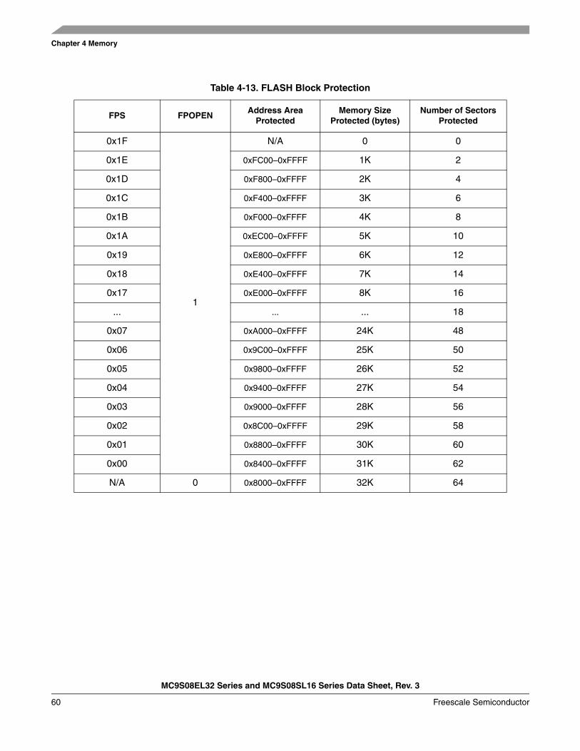
Chapter 4 Memory
MC9S08EL32 Series and MC9S08SL16 Series Data Sheet, Rev. 3
60 Freescale Semiconductor
Table 4-13. FLASH Block Protection
FPS FPOPENAddress Area
ProtectedMemory Size
Protected (bytes)Number of Sectors
Protected
0x1F
1
N/A 0 0
0x1E 0xFC00–0xFFFF 1K 2
0x1D 0xF800–0xFFFF 2K 4
0x1C 0xF400–0xFFFF 3K 6
0x1B 0xF000–0xFFFF 4K 8
0x1A 0xEC00–0xFFFF 5K 10
0x19 0xE800–0xFFFF 6K 12
0x18 0xE400–0xFFFF 7K 14
0x17 0xE000–0xFFFF 8K 16
... ... ... 18
0x07 0xA000–0xFFFF 24K 48
0x06 0x9C00–0xFFFF 25K 50
0x05 0x9800–0xFFFF 26K 52
0x04 0x9400–0xFFFF 27K 54
0x03 0x9000–0xFFFF 28K 56
0x02 0x8C00–0xFFFF 29K 58
0x01 0x8800–0xFFFF 30K 60
0x00 0x8400–0xFFFF 31K 62
N/A 0 0x8000–0xFFFF 32K 64
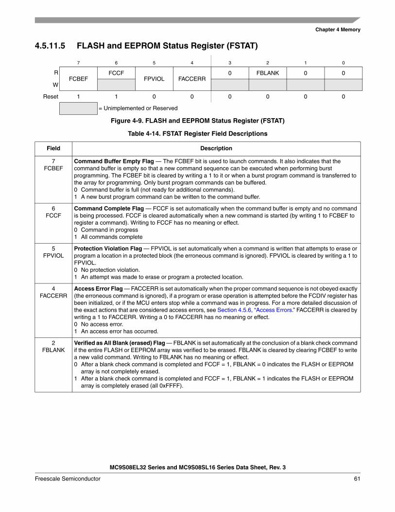
Chapter 4 Memory
MC9S08EL32 Series and MC9S08SL16 Series Data Sheet, Rev. 3
Freescale Semiconductor 61
4.5.11.5 FLASH and EEPROM Status Register (FSTAT)
7 6 5 4 3 2 1 0
RFCBEF
FCCFFPVIOL FACCERR
0 FBLANK 0 0
W
Reset 1 1 0 0 0 0 0 0
= Unimplemented or Reserved
Figure 4-9. FLASH and EEPROM Status Register (FSTAT)
Table 4-14. FSTAT Register Field Descriptions
Field Description
7FCBEF
Command Buffer Empty Flag — The FCBEF bit is used to launch commands. It also indicates that the command buffer is empty so that a new command sequence can be executed when performing burst programming. The FCBEF bit is cleared by writing a 1 to it or when a burst program command is transferred to the array for programming. Only burst program commands can be buffered.0 Command buffer is full (not ready for additional commands).1 A new burst program command can be written to the command buffer.
6FCCF
Command Complete Flag — FCCF is set automatically when the command buffer is empty and no command is being processed. FCCF is cleared automatically when a new command is started (by writing 1 to FCBEF to register a command). Writing to FCCF has no meaning or effect.0 Command in progress1 All commands complete
5FPVIOL
Protection Violation Flag — FPVIOL is set automatically when a command is written that attempts to erase or program a location in a protected block (the erroneous command is ignored). FPVIOL is cleared by writing a 1 to FPVIOL.0 No protection violation.1 An attempt was made to erase or program a protected location.
4FACCERR
Access Error Flag — FACCERR is set automatically when the proper command sequence is not obeyed exactly (the erroneous command is ignored), if a program or erase operation is attempted before the FCDIV register has been initialized, or if the MCU enters stop while a command was in progress. For a more detailed discussion of the exact actions that are considered access errors, see Section 4.5.6, “Access Errors.” FACCERR is cleared by writing a 1 to FACCERR. Writing a 0 to FACCERR has no meaning or effect.0 No access error.1 An access error has occurred.
2FBLANK
Verified as All Blank (erased) Flag — FBLANK is set automatically at the conclusion of a blank check command if the entire FLASH or EEPROM array was verified to be erased. FBLANK is cleared by clearing FCBEF to write a new valid command. Writing to FBLANK has no meaning or effect.0 After a blank check command is completed and FCCF = 1, FBLANK = 0 indicates the FLASH or EEPROM
array is not completely erased.1 After a blank check command is completed and FCCF = 1, FBLANK = 1 indicates the FLASH or EEPROM
array is completely erased (all 0xFFFF).
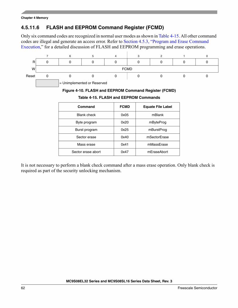
Chapter 4 Memory
MC9S08EL32 Series and MC9S08SL16 Series Data Sheet, Rev. 3
62 Freescale Semiconductor
4.5.11.6 FLASH and EEPROM Command Register (FCMD)
Only six command codes are recognized in normal user modes as shown in Table 4-15. All other command codes are illegal and generate an access error. Refer to Section 4.5.3, “Program and Erase Command Execution,” for a detailed discussion of FLASH and EEPROM programming and erase operations.
It is not necessary to perform a blank check command after a mass erase operation. Only blank check is required as part of the security unlocking mechanism.
7 6 5 4 3 2 1 0
R 0 0 0 0 0 0 0 0
W FCMD
Reset 0 0 0 0 0 0 0 0
= Unimplemented or Reserved
Figure 4-10. FLASH and EEPROM Command Register (FCMD)
Table 4-15. FLASH and EEPROM Commands
Command FCMD Equate File Label
Blank check 0x05 mBlank
Byte program 0x20 mByteProg
Burst program 0x25 mBurstProg
Sector erase 0x40 mSectorErase
Mass erase 0x41 mMassErase
Sector erase abort 0x47 mEraseAbort
MC9S08EL32 Series and MC9S08SL16 Series Data Sheet, Rev. 3
Freescale Semiconductor 63
Chapter 5 Resets, Interrupts, and General System Control
5.1 IntroductionThis section discusses basic reset and interrupt mechanisms and the various sources of reset and interrupt in the MC9S08EL32 Series and MC9S08SL16 Series. Some interrupt sources from peripheral modules are discussed in greater detail within other sections of this data sheet. This section gathers basic information about all reset and interrupt sources in one place for easy reference. A few reset and interrupt sources, including the computer operating properly (COP) watchdog are not part of on-chip peripheral systems with their own chapters.
5.2 FeaturesReset and interrupt features include:
• Multiple sources of reset for flexible system configuration and reliable operation• Reset status register (SRS) to indicate source of most recent reset• Separate interrupt vector for each module (reduces polling overhead) (see Table 5-2)
5.3 MCU ResetResetting the MCU provides a way to start processing from a known set of initial conditions. During reset, most control and status registers are forced to initial values and the program counter is loaded from the reset vector (0xFFFE:0xFFFF). On-chip peripheral modules are disabled and I/O pins are initially configured as general-purpose high-impedance inputs with pull-up devices disabled. The I bit in the condition code register (CCR) is set to block maskable interrupts so the user program has a chance to initialize the stack pointer (SP) and system control settings. SP is forced to 0x00FF at reset.
The MC9S08EL32 Series and MC9S08SL16 Series has eight sources for reset:• Power-on reset (POR)• External pin reset (PIN)• Low-voltage detect (LVD)• Computer operating properly (COP) timer• Illegal opcode detect (ILOP)• Illegal address detect (ILAD)• Background debug forced reset
Each of these sources, with the exception of the background debug forced reset, has an associated bit in the system reset status register (SRS).
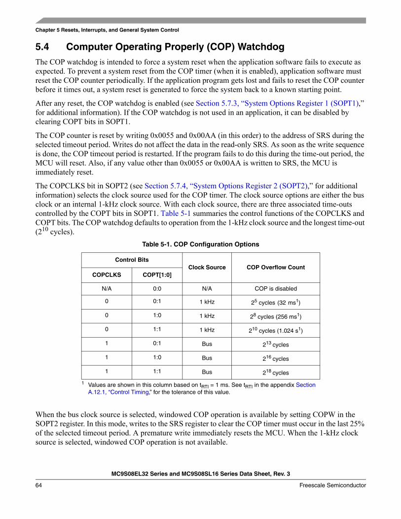
Chapter 5 Resets, Interrupts, and General System Control
MC9S08EL32 Series and MC9S08SL16 Series Data Sheet, Rev. 3
64 Freescale Semiconductor
5.4 Computer Operating Properly (COP) WatchdogThe COP watchdog is intended to force a system reset when the application software fails to execute as expected. To prevent a system reset from the COP timer (when it is enabled), application software must reset the COP counter periodically. If the application program gets lost and fails to reset the COP counter before it times out, a system reset is generated to force the system back to a known starting point.
After any reset, the COP watchdog is enabled (see Section 5.7.3, “System Options Register 1 (SOPT1),” for additional information). If the COP watchdog is not used in an application, it can be disabled by clearing COPT bits in SOPT1.
The COP counter is reset by writing 0x0055 and 0x00AA (in this order) to the address of SRS during the selected timeout period. Writes do not affect the data in the read-only SRS. As soon as the write sequence is done, the COP timeout period is restarted. If the program fails to do this during the time-out period, the MCU will reset. Also, if any value other than 0x0055 or 0x00AA is written to SRS, the MCU is immediately reset.
The COPCLKS bit in SOPT2 (see Section 5.7.4, “System Options Register 2 (SOPT2),” for additional information) selects the clock source used for the COP timer. The clock source options are either the bus clock or an internal 1-kHz clock source. With each clock source, there are three associated time-outs controlled by the COPT bits in SOPT1. Table 5-1 summaries the control functions of the COPCLKS and COPT bits. The COP watchdog defaults to operation from the 1-kHz clock source and the longest time-out (210 cycles).
When the bus clock source is selected, windowed COP operation is available by setting COPW in the SOPT2 register. In this mode, writes to the SRS register to clear the COP timer must occur in the last 25% of the selected timeout period. A premature write immediately resets the MCU. When the 1-kHz clock source is selected, windowed COP operation is not available.
Table 5-1. COP Configuration Options
Control BitsClock Source COP Overflow Count
COPCLKS COPT[1:0]
N/A 0:0 N/A COP is disabled
0 0:1 1 kHz 25 cycles (32 ms1)
1 Values are shown in this column based on tRTI = 1 ms. See tRTI in the appendix Section A.12.1, “Control Timing,” for the tolerance of this value.
0 1:0 1 kHz 28 cycles (256 ms1)
0 1:1 1 kHz 210 cycles (1.024 s1)
1 0:1 Bus 213 cycles
1 1:0 Bus 216 cycles
1 1:1 Bus 218 cycles
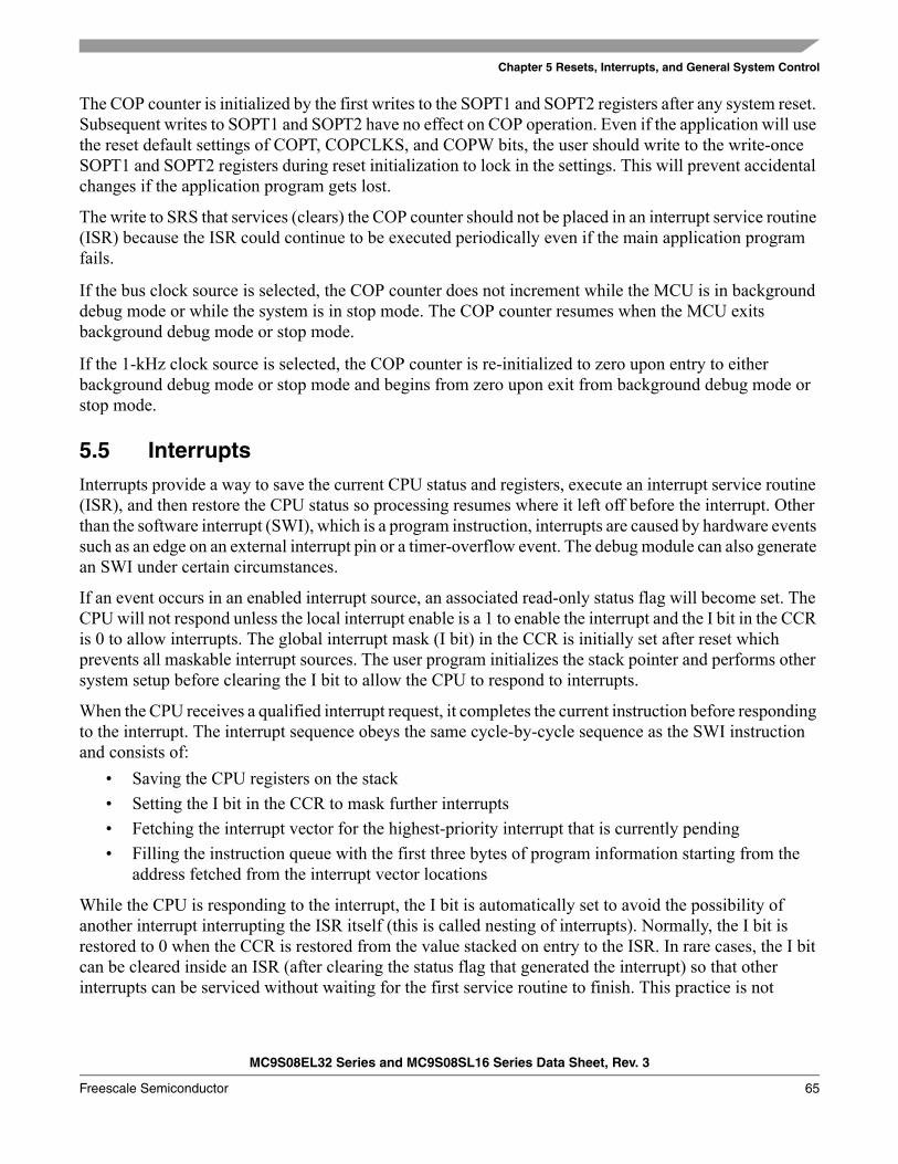
Chapter 5 Resets, Interrupts, and General System Control
MC9S08EL32 Series and MC9S08SL16 Series Data Sheet, Rev. 3
Freescale Semiconductor 65
The COP counter is initialized by the first writes to the SOPT1 and SOPT2 registers after any system reset. Subsequent writes to SOPT1 and SOPT2 have no effect on COP operation. Even if the application will use the reset default settings of COPT, COPCLKS, and COPW bits, the user should write to the write-once SOPT1 and SOPT2 registers during reset initialization to lock in the settings. This will prevent accidental changes if the application program gets lost.
The write to SRS that services (clears) the COP counter should not be placed in an interrupt service routine (ISR) because the ISR could continue to be executed periodically even if the main application program fails.
If the bus clock source is selected, the COP counter does not increment while the MCU is in background debug mode or while the system is in stop mode. The COP counter resumes when the MCU exits background debug mode or stop mode.
If the 1-kHz clock source is selected, the COP counter is re-initialized to zero upon entry to either background debug mode or stop mode and begins from zero upon exit from background debug mode or stop mode.
5.5 InterruptsInterrupts provide a way to save the current CPU status and registers, execute an interrupt service routine (ISR), and then restore the CPU status so processing resumes where it left off before the interrupt. Other than the software interrupt (SWI), which is a program instruction, interrupts are caused by hardware events such as an edge on an external interrupt pin or a timer-overflow event. The debug module can also generate an SWI under certain circumstances.
If an event occurs in an enabled interrupt source, an associated read-only status flag will become set. The CPU will not respond unless the local interrupt enable is a 1 to enable the interrupt and the I bit in the CCR is 0 to allow interrupts. The global interrupt mask (I bit) in the CCR is initially set after reset which prevents all maskable interrupt sources. The user program initializes the stack pointer and performs other system setup before clearing the I bit to allow the CPU to respond to interrupts.
When the CPU receives a qualified interrupt request, it completes the current instruction before responding to the interrupt. The interrupt sequence obeys the same cycle-by-cycle sequence as the SWI instruction and consists of:
• Saving the CPU registers on the stack• Setting the I bit in the CCR to mask further interrupts• Fetching the interrupt vector for the highest-priority interrupt that is currently pending• Filling the instruction queue with the first three bytes of program information starting from the
address fetched from the interrupt vector locations
While the CPU is responding to the interrupt, the I bit is automatically set to avoid the possibility of another interrupt interrupting the ISR itself (this is called nesting of interrupts). Normally, the I bit is restored to 0 when the CCR is restored from the value stacked on entry to the ISR. In rare cases, the I bit can be cleared inside an ISR (after clearing the status flag that generated the interrupt) so that other interrupts can be serviced without waiting for the first service routine to finish. This practice is not
Chapter 5 Resets, Interrupts, and General System Control
MC9S08EL32 Series and MC9S08SL16 Series Data Sheet, Rev. 3
66 Freescale Semiconductor
recommended for anyone other than the most experienced programmers because it can lead to subtle program errors that are difficult to debug.
The interrupt service routine ends with a return-from-interrupt (RTI) instruction which restores the CCR, A, X, and PC registers to their pre-interrupt values by reading the previously saved information from the stack.
NOTEFor compatibility with M68HC08 devices, the H register is not automatically saved and restored. It is good programming practice to push H onto the stack at the start of the interrupt service routine (ISR) and restore it immediately before the RTI that is used to return from the ISR.
If more than one interrupt is pending when the I bit is cleared, the highest priority source is serviced first (see Table 5-2).
5.5.1 Interrupt Stack Frame
Figure 5-1 shows the contents and organization of a stack frame. Before the interrupt, the stack pointer (SP) points at the next available byte location on the stack. The current values of CPU registers are stored on the stack starting with the low-order byte of the program counter (PCL) and ending with the CCR. After stacking, the SP points at the next available location on the stack which is the address that is one less than the address where the CCR was saved. The PC value that is stacked is the address of the instruction in the main program that would have executed next if the interrupt had not occurred.
Figure 5-1. Interrupt Stack Frame
When an RTI instruction is executed, these values are recovered from the stack in reverse order. As part of the RTI sequence, the CPU fills the instruction pipeline by reading three bytes of program information, starting from the PC address recovered from the stack.
CONDITION CODE REGISTER
ACCUMULATOR
INDEX REGISTER (LOW BYTE X)
PROGRAM COUNTER HIGH
* High byte (H) of index register is not automatically stacked.
*
PROGRAM COUNTER LOW
²
²
²
²7 0
UNSTACKINGORDER
STACKINGORDER
5
4
3
2
1
1
2
3
4
5
TOWARD LOWER ADDRESSES
TOWARD HIGHER ADDRESSES
SP BEFORE
SP AFTERINTERRUPT STACKING
THE INTERRUPT
Chapter 5 Resets, Interrupts, and General System Control
MC9S08EL32 Series and MC9S08SL16 Series Data Sheet, Rev. 3
Freescale Semiconductor 67
The status flag corresponding to the interrupt source must be acknowledged (cleared) before returning from the ISR. Typically, the flag is cleared at the beginning of the ISR so that if another interrupt is generated by this same source, it will be registered so it can be serviced after completion of the current ISR.
5.5.2 Interrupt Vectors, Sources, and Local Masks
Table 5-2 provides a summary of all interrupt sources. Higher-priority sources are located toward the bottom of the table. The high-order byte of the address for the interrupt service routine is located at the first address in the vector address column, and the low-order byte of the address for the interrupt service routine is located at the next higher address.
When an interrupt condition occurs, an associated flag bit becomes set. If the associated local interrupt enable is 1, an interrupt request is sent to the CPU. Within the CPU, if the global interrupt mask (I bit in the CCR) is 0, the CPU will finish the current instruction; stack the PCL, PCH, X, A, and CCR CPU registers; set the I bit; and then fetch the interrupt vector for the highest priority pending interrupt. Processing then continues in the interrupt service routine.
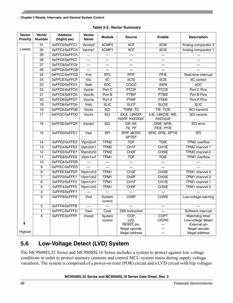
Chapter 5 Resets, Interrupts, and General System Control
MC9S08EL32 Series and MC9S08SL16 Series Data Sheet, Rev. 3
68 Freescale Semiconductor
5.6 Low-Voltage Detect (LVD) SystemThe MC9S08EL32 Series and MC9S08SL16 Series includes a system to protect against low voltage conditions in order to protect memory contents and control MCU system states during supply voltage variations. The system is comprised of a power-on reset (POR) circuit and a LVD circuit with trip voltages
Table 5-2. Vector Summary
Vector Priority
Vector Number
Address(High/Low)
Vector Name
Module Source Enable Description
Lowest
Highest
31 0xFFC0/0xFFC1 Vacmp2 ACMP2 ACF ACIE Analog comparator 230 0xFFC2/0xFFC3 Vacmp1 ACMP1 ACF ACIE Analog comparator 1
29 0xFFC4/0xFFC5 — — — — —
28 0xFFC6/0xFFC7 — — — — —
27 0xFFC8/0xFFC9 — — — — —26 0xFFCA/0xFFCB — — — — —
25 0xFFCC/0xFFCD Vrtc RTC RTIF RTIE Real-time interrupt
24 0xFFCE/0xFFCF Viic IIC IICIS IICIE IIC control23 0xFFD0/0xFFD1 Vadc ADC COCO AIEN ADC
22 0xFFD2/0xFFD3 Vportc Port C PTCIF PTCIE Port C Pins
21 0xFFD4/0xFFD5 Vportb Port B PTBIF PTBIE Port B Pins20 0xFFD6/0xFFD7 Vporta Port A PTAIF PTAIE Port A Pins
19 0xFFD8/0xFFD9 Vslic SLIC SLCF SLCIE SLIC
18 0xFFDA/0xFFDB Vscitx SCI TDRE, TC TIE, TCIE SCI transmit17 0xFFDC/0xFFDD Vscirx SCI IDLE, LBKDIF,
RDRF, RXEDGIFILIE, LBKDIE, RIE,
RXEDGIESCI receive
16 0xFFDE/0xFFDF Vscierr SCI OR, NF,FE, PF
ORIE, NFIE,FEIE, PFIE
SCI error
15 0xFFE0/0xFFE1 Vspi SPI SPIF, MODF,SPTEF
SPIE, SPIE, SPTIE SPI
14 0xFFE2/0xFFE3 Vtpm2ovf TPM2 TOF TOIE TPM2 overflow
13 0xFFE4/0xFFE5 Vtpm2ch1 TPM2 CH1F CH1IE TPM2 channel 1
12 0xFFE6/0xFFE7 Vtpm2ch0 TPM2 CH0F CH0IE TPM2 channel 011 0xFFE8/0xFFE9 Vtpm1ovf TPM1 TOF TOIE TPM1 overflow
10 0xFFEA/0xFFEB — — — — —
9 0xFFEC/0xFFED — — — — —8 0xFFEE/0xFFEF Vtpm1ch3 TPM1 CH3F CH3IE TPM1 channel 3
7 0xFFF0/0xFFF1 Vtpm1ch2 TPM1 CH2F CH2IE TPM1 channel 2
6 0xFFF2/0xFFF3 Vtpm1ch1 TPM1 CH1F CH1IE TPM1 channel 15 0xFFF4/0xFFF5 Vtpm1ch0 TPM1 CH0F CH0IE TPM1 channel 0
4 0xFFF6/0xFFF7 — — — — —
3 0xFFF8/0xFFF9 Vlvd Systemcontrol
LVWF LVWIE Low-voltage warning
2 0xFFFA/0xFFFB — — — — —1 0xFFFC/0xFFFD Vswi Core SWI Instruction — Software interrupt
0 0xFFFE/0xFFFF Vreset Systemcontrol
COP,LVD,
RESET pin,Illegal opcode,Illegal address
COPTLVDRE
———
Watchdog timerLow-voltage detect
External pinIllegal opcodeIllegal address
Chapter 5 Resets, Interrupts, and General System Control
MC9S08EL32 Series and MC9S08SL16 Series Data Sheet, Rev. 3
Freescale Semiconductor 69
for warning and detection. The LVD circuit is enabled when LVDE in SPMSC1 is set to 1. The LVD is disabled upon entering any of the stop modes unless LVDSE is set in SPMSC1. If LVDSE and LVDE are both set, then the MCU cannot enter stop2, and the current consumption in stop3 with the LVD enabled will be higher.
5.6.1 Power-On Reset Operation
When power is initially applied to the MCU, or when the supply voltage drops below the power-on reset rearm voltage level, VPOR, the POR circuit will cause a reset condition. As the supply voltage rises, the LVD circuit will hold the MCU in reset until the supply has risen above the low voltage detection low threshold, VLVDL. Both the POR bit and the LVD bit in SRS are set following a POR.
5.6.2 Low-Voltage Detection (LVD) Reset Operation
The LVD can be configured to generate a reset upon detection of a low voltage condition by setting LVDRE to 1. The low voltage detection threshold is determined by the LVDV bit. After an LVD reset has occurred, the LVD system will hold the MCU in reset until the supply voltage has risen above the low voltage detection threshold. The LVD bit in the SRS register is set following either an LVD reset or POR.
5.6.3 Low-Voltage Warning (LVW) Interrupt Operation
The LVD system has a low voltage warning flag to indicate to the user that the supply voltage is approaching the low voltage condition. When a low voltage warning condition is detected and is configured for interrupt operation (LVWIE set to 1), LVWF in SPMSC1 will be set and an LVW interrupt request will occur.
Chapter 5 Resets, Interrupts, and General System Control
MC9S08EL32 Series and MC9S08SL16 Series Data Sheet, Rev. 3
70 Freescale Semiconductor
5.7 Reset, Interrupt, and System Control Registers and Control BitsOne 8-bit register in the direct page register space and eight 8-bit registers in the high-page register space are related to reset and interrupt systems.
Refer to Table 4-2 and Table 4-3 in Chapter 4, “Memory,” of this data sheet for the absolute address assignments for all registers. This section refers to registers and control bits only by their names. A Freescale-provided equate or header file is used to translate these names into the appropriate absolute addresses.
Some control bits in the SOPT1 and SPMSC2 registers are related to modes of operation. Although brief descriptions of these bits are provided here, the related functions are discussed in greater detail in Chapter 3, “Modes of Operation.”
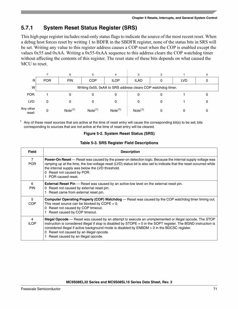
Chapter 5 Resets, Interrupts, and General System Control
MC9S08EL32 Series and MC9S08SL16 Series Data Sheet, Rev. 3
Freescale Semiconductor 71
5.7.1 System Reset Status Register (SRS)
This high page register includes read-only status flags to indicate the source of the most recent reset. When a debug host forces reset by writing 1 to BDFR in the SBDFR register, none of the status bits in SRS will be set. Writing any value to this register address causes a COP reset when the COP is enabled except the values 0x55 and 0xAA. Writing a 0x55-0xAA sequence to this address clears the COP watchdog timer without affecting the contents of this register. The reset state of these bits depends on what caused the MCU to reset.
Figure 5-2. System Reset Status (SRS)
7 6 5 4 3 2 1 0
R POR PIN COP ILOP ILAD 0 LVD 0
W Writing 0x55, 0xAA to SRS address clears COP watchdog timer.
POR: 1 0 0 0 0 0 1 0
LVD: 0 0 0 0 0 0 1 0
Any otherreset:
0 Note(1)
1 Any of these reset sources that are active at the time of reset entry will cause the corresponding bit(s) to be set; bits corresponding to sources that are not active at the time of reset entry will be cleared.
Note(1) Note(1) Note(1) 0 0 0
Table 5-3. SRS Register Field Descriptions
Field Description
7POR
Power-On Reset — Reset was caused by the power-on detection logic. Because the internal supply voltage was ramping up at the time, the low-voltage reset (LVD) status bit is also set to indicate that the reset occurred while the internal supply was below the LVD threshold.0 Reset not caused by POR.1 POR caused reset.
6PIN
External Reset Pin — Reset was caused by an active-low level on the external reset pin.0 Reset not caused by external reset pin.1 Reset came from external reset pin.
5COP
Computer Operating Properly (COP) Watchdog — Reset was caused by the COP watchdog timer timing out. This reset source can be blocked by COPE = 0.0 Reset not caused by COP timeout.1 Reset caused by COP timeout.
4ILOP
Illegal Opcode — Reset was caused by an attempt to execute an unimplemented or illegal opcode. The STOP instruction is considered illegal if stop is disabled by STOPE = 0 in the SOPT register. The BGND instruction is considered illegal if active background mode is disabled by ENBDM = 0 in the BDCSC register.0 Reset not caused by an illegal opcode.1 Reset caused by an illegal opcode.
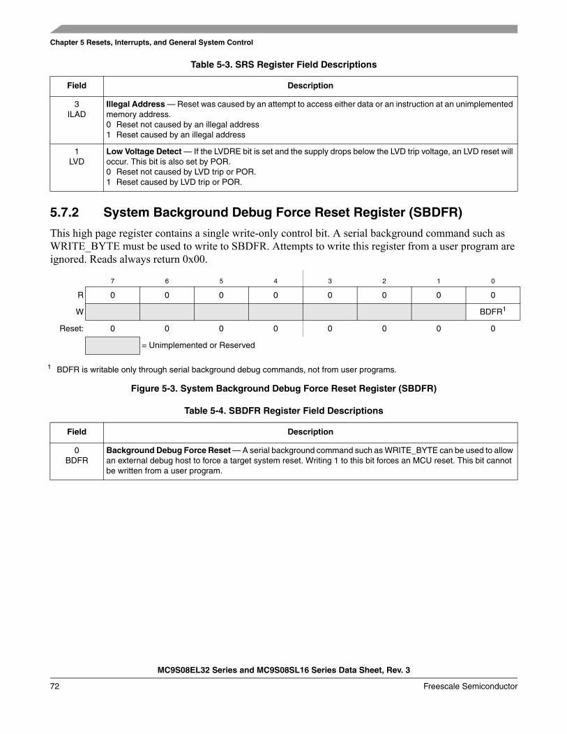
Chapter 5 Resets, Interrupts, and General System Control
MC9S08EL32 Series and MC9S08SL16 Series Data Sheet, Rev. 3
72 Freescale Semiconductor
5.7.2 System Background Debug Force Reset Register (SBDFR)
This high page register contains a single write-only control bit. A serial background command such as WRITE_BYTE must be used to write to SBDFR. Attempts to write this register from a user program are ignored. Reads always return 0x00.
Figure 5-3. System Background Debug Force Reset Register (SBDFR)
3ILAD
Illegal Address — Reset was caused by an attempt to access either data or an instruction at an unimplemented memory address.0 Reset not caused by an illegal address1 Reset caused by an illegal address
1LVD
Low Voltage Detect — If the LVDRE bit is set and the supply drops below the LVD trip voltage, an LVD reset will occur. This bit is also set by POR.0 Reset not caused by LVD trip or POR.1 Reset caused by LVD trip or POR.
7 6 5 4 3 2 1 0
R 0 0 0 0 0 0 0 0
W BDFR1
1 BDFR is writable only through serial background debug commands, not from user programs.
Reset: 0 0 0 0 0 0 0 0
= Unimplemented or Reserved
Table 5-4. SBDFR Register Field Descriptions
Field Description
0BDFR
Background Debug Force Reset — A serial background command such as WRITE_BYTE can be used to allow an external debug host to force a target system reset. Writing 1 to this bit forces an MCU reset. This bit cannot be written from a user program.
Table 5-3. SRS Register Field Descriptions
Field Description
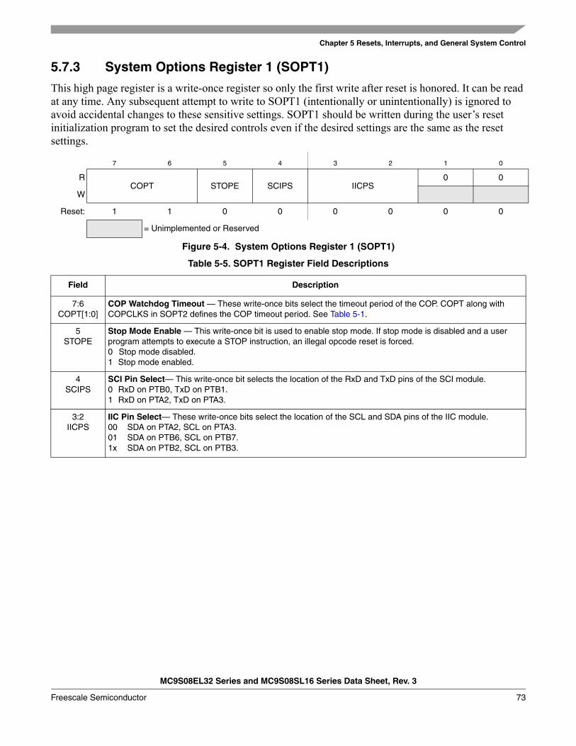
Chapter 5 Resets, Interrupts, and General System Control
MC9S08EL32 Series and MC9S08SL16 Series Data Sheet, Rev. 3
Freescale Semiconductor 73
5.7.3 System Options Register 1 (SOPT1)
This high page register is a write-once register so only the first write after reset is honored. It can be read at any time. Any subsequent attempt to write to SOPT1 (intentionally or unintentionally) is ignored to avoid accidental changes to these sensitive settings. SOPT1 should be written during the user’s reset initialization program to set the desired controls even if the desired settings are the same as the reset settings.
7 6 5 4 3 2 1 0
RCOPT STOPE SCIPS IICPS
0 0
W
Reset: 1 1 0 0 0 0 0 0
= Unimplemented or Reserved
Figure 5-4. System Options Register 1 (SOPT1)
Table 5-5. SOPT1 Register Field Descriptions
Field Description
7:6COPT[1:0]
COP Watchdog Timeout — These write-once bits select the timeout period of the COP. COPT along with COPCLKS in SOPT2 defines the COP timeout period. See Table 5-1.
5STOPE
Stop Mode Enable — This write-once bit is used to enable stop mode. If stop mode is disabled and a user program attempts to execute a STOP instruction, an illegal opcode reset is forced.0 Stop mode disabled.1 Stop mode enabled.
4SCIPS
SCI Pin Select— This write-once bit selects the location of the RxD and TxD pins of the SCI module.0 RxD on PTB0, TxD on PTB1.1 RxD on PTA2, TxD on PTA3.
3:2IICPS
IIC Pin Select— These write-once bits select the location of the SCL and SDA pins of the IIC module.00 SDA on PTA2, SCL on PTA3.01 SDA on PTB6, SCL on PTB7.1x SDA on PTB2, SCL on PTB3.
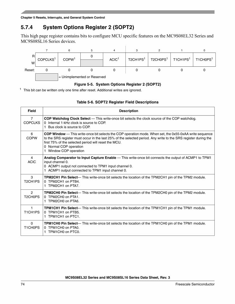
Chapter 5 Resets, Interrupts, and General System Control
MC9S08EL32 Series and MC9S08SL16 Series Data Sheet, Rev. 3
74 Freescale Semiconductor
5.7.4 System Options Register 2 (SOPT2)
This high page register contains bits to configure MCU specific features on the MC9S08EL32 Series and MC9S08SL16 Series devices.
7 6 5 4 3 2 1 0
RCOPCLKS1
1 This bit can be written only one time after reset. Additional writes are ignored.
COPW10
ACIC1 T2CH1PS1 T2CH0PS1 T1CH1PS1 T1CH0PS1
W
Reset: 0 0 0 0 0 0 0 0
= Unimplemented or Reserved
Figure 5-5. System Options Register 2 (SOPT2)
Table 5-6. SOPT2 Register Field Descriptions
Field Description
7COPCLKS
COP Watchdog Clock Select — This write-once bit selects the clock source of the COP watchdog.0 Internal 1-kHz clock is source to COP.1 Bus clock is source to COP.
6COPW
COP Window — This write-once bit selects the COP operation mode. When set, the 0x55-0xAA write sequence to the SRS register must occur in the last 25% of the selected period. Any write to the SRS register during the first 75% of the selected period will reset the MCU.0 Normal COP operation1 Window COP operation
4ACIC
Analog Comparator to Input Capture Enable — This write-once bit connects the output of ACMP1 to TPM1 input channel 0.0 ACMP1 output not connected to TPM1 input channel 0.1 ACMP1 output connected to TPM1 input channel 0.
3T2CH1PS
TPM2CH1 Pin Select— This write-once bit selects the location of the TPM2CH1 pin of the TPM2 module.0 TPM2CH1 on PTB4.1 TPM2CH1 on PTA7.
2T2CH0PS
TPM2CH0 Pin Select— This write-once bit selects the location of the TPM2CH0 pin of the TPM2 module.0 TPM2CH0 on PTA1.1 TPM2CH0 on PTA6.
1T1CH1PS
TPM1CH1 Pin Select— This write-once bit selects the location of the TPM1CH1 pin of the TPM1 module.0 TPM1CH1 on PTB5.1 TPM1CH1 on PTC1.
0T1CH0PS
TPM1CH0 Pin Select— This write-once bit selects the location of the TPM1CH0 pin of the TPM1 module.0 TPM1CH0 on PTA0.1 TPM1CH0 on PTC0.
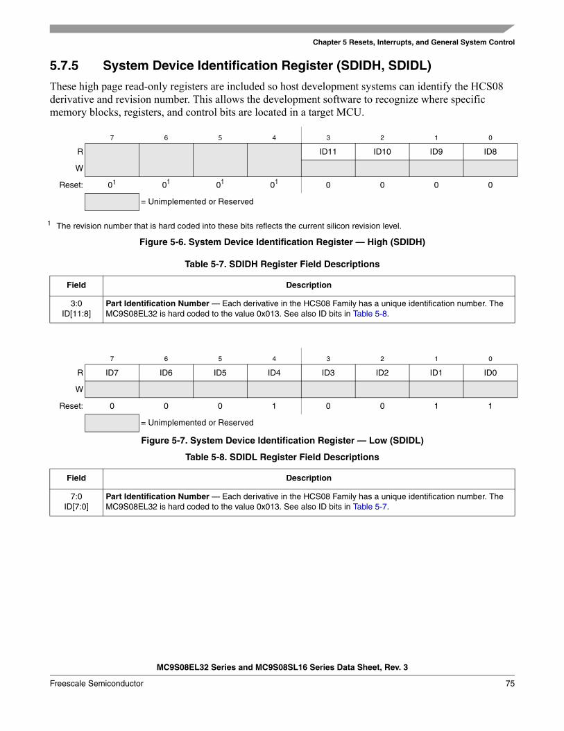
Chapter 5 Resets, Interrupts, and General System Control
MC9S08EL32 Series and MC9S08SL16 Series Data Sheet, Rev. 3
Freescale Semiconductor 75
5.7.5 System Device Identification Register (SDIDH, SDIDL)
These high page read-only registers are included so host development systems can identify the HCS08 derivative and revision number. This allows the development software to recognize where specific memory blocks, registers, and control bits are located in a target MCU.
Figure 5-6. System Device Identification Register — High (SDIDH)
7 6 5 4 3 2 1 0
R ID11 ID10 ID9 ID8
W
Reset: 01
1 The revision number that is hard coded into these bits reflects the current silicon revision level.
01 01 01 0 0 0 0
= Unimplemented or Reserved
Table 5-7. SDIDH Register Field Descriptions
Field Description
3:0ID[11:8]
Part Identification Number — Each derivative in the HCS08 Family has a unique identification number. The MC9S08EL32 is hard coded to the value 0x013. See also ID bits in Table 5-8.
7 6 5 4 3 2 1 0
R ID7 ID6 ID5 ID4 ID3 ID2 ID1 ID0
W
Reset: 0 0 0 1 0 0 1 1
= Unimplemented or Reserved
Figure 5-7. System Device Identification Register — Low (SDIDL)
Table 5-8. SDIDL Register Field Descriptions
Field Description
7:0ID[7:0]
Part Identification Number — Each derivative in the HCS08 Family has a unique identification number. The MC9S08EL32 is hard coded to the value 0x013. See also ID bits in Table 5-7.
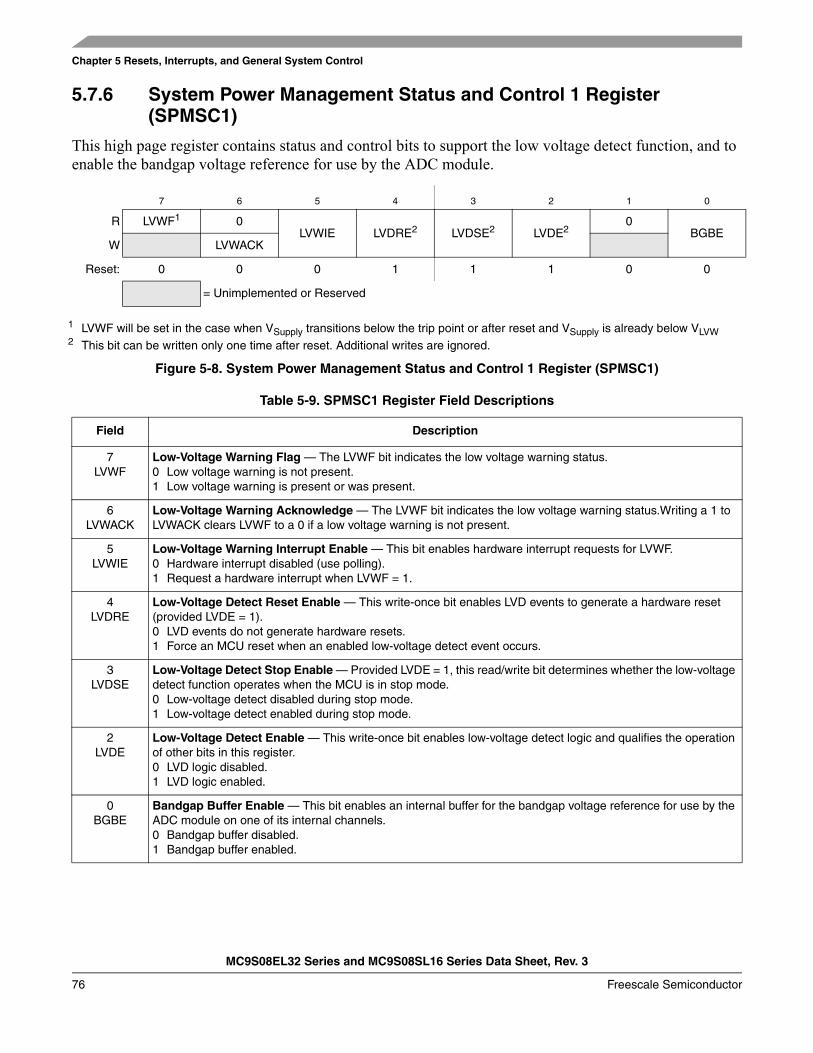
Chapter 5 Resets, Interrupts, and General System Control
MC9S08EL32 Series and MC9S08SL16 Series Data Sheet, Rev. 3
76 Freescale Semiconductor
5.7.6 System Power Management Status and Control 1 Register (SPMSC1)
This high page register contains status and control bits to support the low voltage detect function, and to enable the bandgap voltage reference for use by the ADC module.
Figure 5-8. System Power Management Status and Control 1 Register (SPMSC1)
7 6 5 4 3 2 1 0
R LVWF1
1 LVWF will be set in the case when VSupply transitions below the trip point or after reset and VSupply is already below VLVW
0LVWIE LVDRE2
2 This bit can be written only one time after reset. Additional writes are ignored.
LVDSE2 LVDE20
BGBEW LVWACK
Reset: 0 0 0 1 1 1 0 0
= Unimplemented or Reserved
Table 5-9. SPMSC1 Register Field Descriptions
Field Description
7LVWF
Low-Voltage Warning Flag — The LVWF bit indicates the low voltage warning status.0 Low voltage warning is not present.1 Low voltage warning is present or was present.
6LVWACK
Low-Voltage Warning Acknowledge — The LVWF bit indicates the low voltage warning status.Writing a 1 to LVWACK clears LVWF to a 0 if a low voltage warning is not present.
5LVWIE
Low-Voltage Warning Interrupt Enable — This bit enables hardware interrupt requests for LVWF.0 Hardware interrupt disabled (use polling).1 Request a hardware interrupt when LVWF = 1.
4LVDRE
Low-Voltage Detect Reset Enable — This write-once bit enables LVD events to generate a hardware reset (provided LVDE = 1). 0 LVD events do not generate hardware resets.1 Force an MCU reset when an enabled low-voltage detect event occurs.
3LVDSE
Low-Voltage Detect Stop Enable — Provided LVDE = 1, this read/write bit determines whether the low-voltage detect function operates when the MCU is in stop mode.0 Low-voltage detect disabled during stop mode.1 Low-voltage detect enabled during stop mode.
2LVDE
Low-Voltage Detect Enable — This write-once bit enables low-voltage detect logic and qualifies the operation of other bits in this register. 0 LVD logic disabled.1 LVD logic enabled.
0BGBE
Bandgap Buffer Enable — This bit enables an internal buffer for the bandgap voltage reference for use by the ADC module on one of its internal channels.0 Bandgap buffer disabled.1 Bandgap buffer enabled.
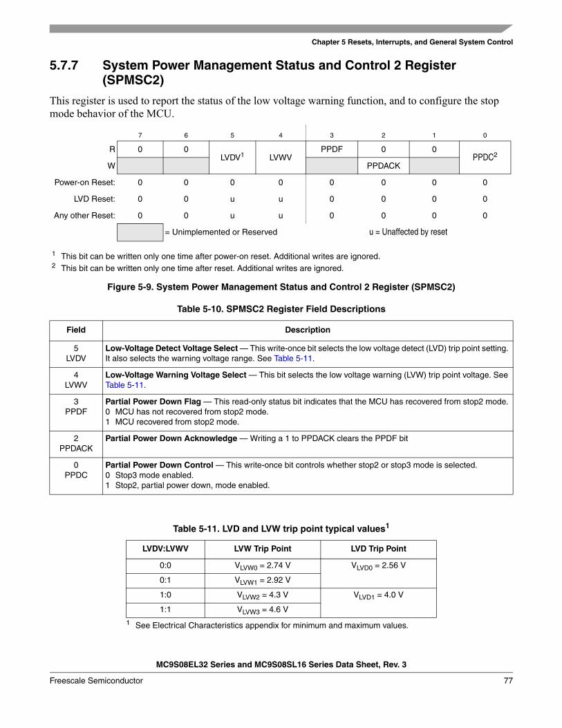
Chapter 5 Resets, Interrupts, and General System Control
MC9S08EL32 Series and MC9S08SL16 Series Data Sheet, Rev. 3
Freescale Semiconductor 77
5.7.7 System Power Management Status and Control 2 Register (SPMSC2)
This register is used to report the status of the low voltage warning function, and to configure the stop mode behavior of the MCU.
Figure 5-9. System Power Management Status and Control 2 Register (SPMSC2)
7 6 5 4 3 2 1 0
R 0 0LVDV1
1 This bit can be written only one time after power-on reset. Additional writes are ignored.
LVWVPPDF 0 0
PPDC2
2 This bit can be written only one time after reset. Additional writes are ignored.
W PPDACK
Power-on Reset: 0 0 0 0 0 0 0 0
LVD Reset: 0 0 u u 0 0 0 0
Any other Reset: 0 0 u u 0 0 0 0
= Unimplemented or Reserved u = Unaffected by reset
Table 5-10. SPMSC2 Register Field Descriptions
Field Description
5LVDV
Low-Voltage Detect Voltage Select — This write-once bit selects the low voltage detect (LVD) trip point setting. It also selects the warning voltage range. See Table 5-11.
4LVWV
Low-Voltage Warning Voltage Select — This bit selects the low voltage warning (LVW) trip point voltage. See Table 5-11.
3PPDF
Partial Power Down Flag — This read-only status bit indicates that the MCU has recovered from stop2 mode.0 MCU has not recovered from stop2 mode.1 MCU recovered from stop2 mode.
2PPDACK
Partial Power Down Acknowledge — Writing a 1 to PPDACK clears the PPDF bit
0PPDC
Partial Power Down Control — This write-once bit controls whether stop2 or stop3 mode is selected.0 Stop3 mode enabled.1 Stop2, partial power down, mode enabled.
Table 5-11. LVD and LVW trip point typical values1
1 See Electrical Characteristics appendix for minimum and maximum values.
LVDV:LVWV LVW Trip Point LVD Trip Point
0:0 VLVW0 = 2.74 V VLVD0 = 2.56 V
0:1 VLVW1 = 2.92 V
1:0 VLVW2 = 4.3 V VLVD1 = 4.0 V
1:1 VLVW3 = 4.6 V

Chapter 5 Resets, Interrupts, and General System Control
MC9S08EL32 Series and MC9S08SL16 Series Data Sheet, Rev. 3
78 Freescale Semiconductor
MC9S08EL32 Series and MC9S08SL16 Series Data Sheet, Rev. 3
Freescale Semiconductor 79
Chapter 6 Parallel Input/Output ControlThis section explains software controls related to parallel input/output (I/O) and pin control. The MC9S08EL32 has three parallel I/O ports which include a total of 22 I/O pins. See Chapter 2, “Pins and Connections,” for more information about pin assignments and external hardware considerations of these pins.
Many of these pins are shared with on-chip peripherals such as timer systems, communication systems, or keyboard interrupts as shown in Table 2-1. The peripheral modules have priority over the general-purpose I/O functions so that when a peripheral is enabled, the I/O functions associated with the shared pins are disabled.
After reset, the shared peripheral functions are disabled and the pins are configured as inputs (PTxDDn = 0). The pin control functions for each pin are configured as follows: slew rate control enabled (PTxSEn = 1), low drive strength selected (PTxDSn = 0), and internal pull-ups disabled (PTxPEn = 0).
NOTENot all general-purpose I/O pins are available on all packages. To avoid extra current drain from floating input pins, the user’s reset initialization routine in the application program must either enable on-chip pull-up devices or change the direction of unconnected pins to outputs so the pins do not float.
6.1 Port Data and Data DirectionReading and writing of parallel I/Os are performed through the port data registers. The direction, either input or output, is controlled through the port data direction registers. The parallel I/O port function for an individual pin is illustrated in the block diagram shown in Figure 6-1.
The data direction control bit (PTxDDn) determines whether the output buffer for the associated pin is enabled, and also controls the source for port data register reads. The input buffer for the associated pin is always enabled unless the pin is enabled as an analog function or is an output-only pin.
When a shared digital function is enabled for a pin, the output buffer is controlled by the shared function. However, the data direction register bit will continue to control the source for reads of the port data register.
When a shared analog function is enabled for a pin, both the input and output buffers are disabled. A value of 0 is read for any port data bit where the bit is an input (PTxDDn = 0) and the input buffer is disabled. In general, whenever a pin is shared with both an alternate digital function and an analog function, the analog function has priority such that if both the digital and analog functions are enabled, the analog function controls the pin.
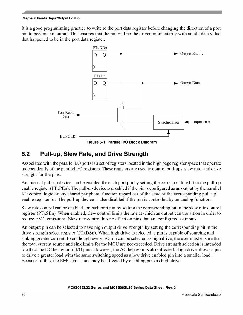
Chapter 6 Parallel Input/Output Control
MC9S08EL32 Series and MC9S08SL16 Series Data Sheet, Rev. 3
80 Freescale Semiconductor
It is a good programming practice to write to the port data register before changing the direction of a port pin to become an output. This ensures that the pin will not be driven momentarily with an old data value that happened to be in the port data register.
Figure 6-1. Parallel I/O Block Diagram
6.2 Pull-up, Slew Rate, and Drive StrengthAssociated with the parallel I/O ports is a set of registers located in the high page register space that operate independently of the parallel I/O registers. These registers are used to control pull-ups, slew rate, and drive strength for the pins.
An internal pull-up device can be enabled for each port pin by setting the corresponding bit in the pull-up enable register (PTxPEn). The pull-up device is disabled if the pin is configured as an output by the parallel I/O control logic or any shared peripheral function regardless of the state of the corresponding pull-up enable register bit. The pull-up device is also disabled if the pin is controlled by an analog function.
Slew rate control can be enabled for each port pin by setting the corresponding bit in the slew rate control register (PTxSEn). When enabled, slew control limits the rate at which an output can transition in order to reduce EMC emissions. Slew rate control has no effect on pins that are configured as inputs.
An output pin can be selected to have high output drive strength by setting the corresponding bit in the drive strength select register (PTxDSn). When high drive is selected, a pin is capable of sourcing and sinking greater current. Even though every I/O pin can be selected as high drive, the user must ensure that the total current source and sink limits for the MCU are not exceeded. Drive strength selection is intended to affect the DC behavior of I/O pins. However, the AC behavior is also affected. High drive allows a pin to drive a greater load with the same switching speed as a low drive enabled pin into a smaller load. Because of this, the EMC emissions may be affected by enabling pins as high drive.
QD
QD
1
0
Port Read
PTxDDn
PTxDn
Output Enable
Output Data
Input DataSynchronizerData
BUSCLK
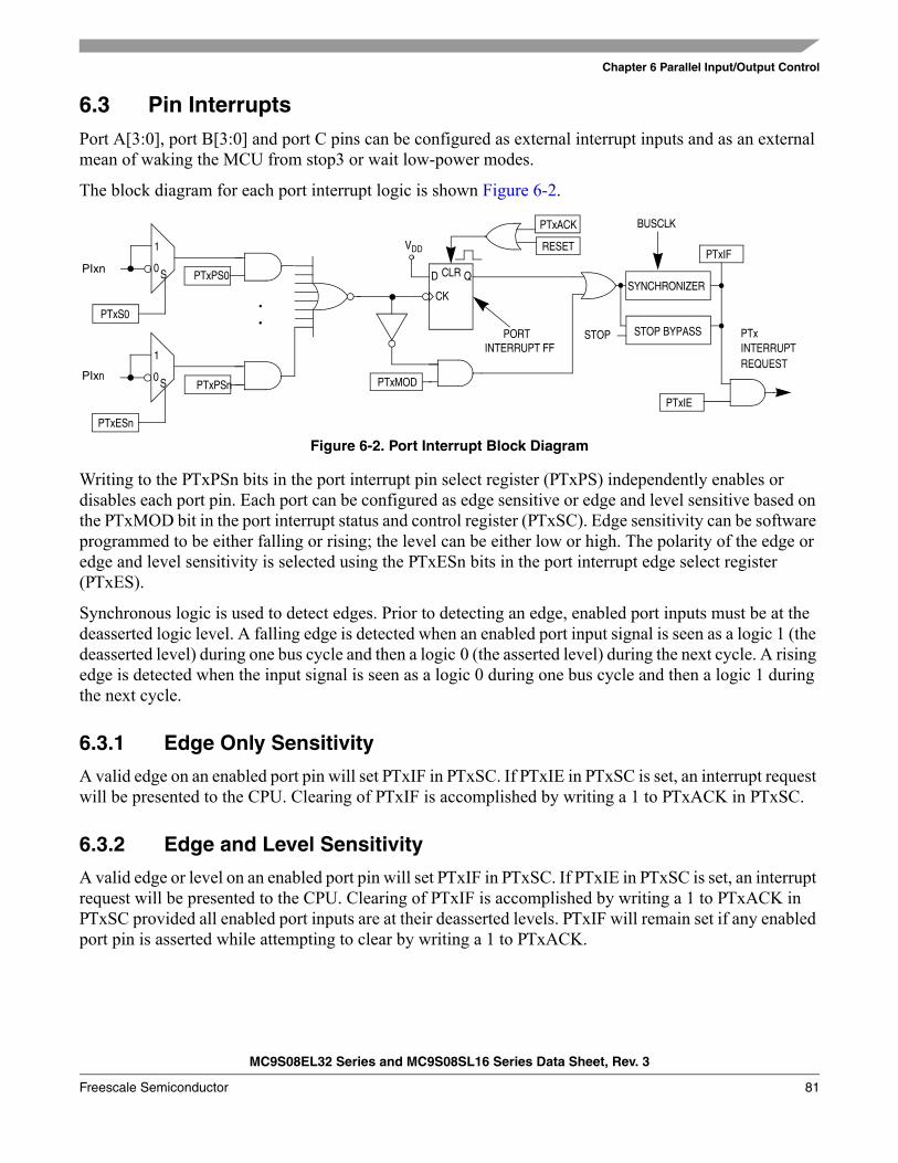
Chapter 6 Parallel Input/Output Control
MC9S08EL32 Series and MC9S08SL16 Series Data Sheet, Rev. 3
Freescale Semiconductor 81
6.3 Pin InterruptsPort A[3:0], port B[3:0] and port C pins can be configured as external interrupt inputs and as an external mean of waking the MCU from stop3 or wait low-power modes.
The block diagram for each port interrupt logic is shown Figure 6-2.
Figure 6-2. Port Interrupt Block Diagram
Writing to the PTxPSn bits in the port interrupt pin select register (PTxPS) independently enables or disables each port pin. Each port can be configured as edge sensitive or edge and level sensitive based on the PTxMOD bit in the port interrupt status and control register (PTxSC). Edge sensitivity can be software programmed to be either falling or rising; the level can be either low or high. The polarity of the edge or edge and level sensitivity is selected using the PTxESn bits in the port interrupt edge select register (PTxES).
Synchronous logic is used to detect edges. Prior to detecting an edge, enabled port inputs must be at the deasserted logic level. A falling edge is detected when an enabled port input signal is seen as a logic 1 (the deasserted level) during one bus cycle and then a logic 0 (the asserted level) during the next cycle. A rising edge is detected when the input signal is seen as a logic 0 during one bus cycle and then a logic 1 during the next cycle.
6.3.1 Edge Only Sensitivity
A valid edge on an enabled port pin will set PTxIF in PTxSC. If PTxIE in PTxSC is set, an interrupt request will be presented to the CPU. Clearing of PTxIF is accomplished by writing a 1 to PTxACK in PTxSC.
6.3.2 Edge and Level Sensitivity
A valid edge or level on an enabled port pin will set PTxIF in PTxSC. If PTxIE in PTxSC is set, an interrupt request will be presented to the CPU. Clearing of PTxIF is accomplished by writing a 1 to PTxACK in PTxSC provided all enabled port inputs are at their deasserted levels. PTxIF will remain set if any enabled port pin is asserted while attempting to clear by writing a 1 to PTxACK.
PTxESn
D Q
CK
CLR
VDD
PTxMOD
PTxIE
PORTINTERRUPT FF
PTxACK
RESET
SYNCHRONIZER
PTxIF
STOP BYPASSSTOP
BUSCLK
PTxPSn0
1
S
PTxPS00
1
S
PTxS0
PIxn
PIxn
PTxINTERRUPTREQUEST
Chapter 6 Parallel Input/Output Control
MC9S08EL32 Series and MC9S08SL16 Series Data Sheet, Rev. 3
82 Freescale Semiconductor
6.3.3 Pull-up/Pull-down Resistors
The port interrupt pins can be configured to use an internal pull-up/pull-down resistor using the associated I/O port pull enable register. If an internal resistor is enabled (PTxPEn=1) and the pin is selected for interrupt (PTxPSn=1), the PTxES register is used to select whether the resistor is a pull-up (PTxESn = 0) or a pull-down (PTxESn = 1).
6.3.4 Pin Interrupt Initialization
When an interrupt pin is first enabled, it is possible to get a false interrupt flag. To prevent a false interrupt request during pin interrupt initialization, the user should do the following:
1. Mask interrupts by clearing PTxIE in PTxSC.2. Select the pin polarity by setting the appropriate PTxESn bits in PTxES.3. If using internal pull-up/pull-down device, configure the associated pull enable bits in PTxPE.4. Enable the interrupt pins by setting the appropriate PTxPSn bits in PTxPS.5. Write to PTxACK in PTxSC to clear any false interrupts.6. Set PTxIE in PTxSC to enable interrupts.
6.4 Pin Behavior in Stop ModesPin behavior following execution of a STOP instruction depends on the stop mode that is entered. An explanation of pin behavior for the various stop modes follows:
• Stop2 mode is a partial power-down mode, whereby I/O latches are maintained in their state as before the STOP instruction was executed. CPU register status and the state of I/O registers should be saved in RAM before the STOP instruction is executed to place the MCU in stop2 mode. Upon recovery from stop2 mode, before accessing any I/O, the user should examine the state of the PPDF bit in the SPMSC2 register. If the PPDF bit is 0, I/O must be initialized as if a power on reset had occurred. If the PPDF bit is 1, I/O data previously stored in RAM, before the STOP instruction was executed, peripherals may require being initialized and restored to their pre-stop condition. The user must then write a 1 to the PPDACK bit in the SPMSC2 register. Access to I/O is now permitted again in the user application program.
• In stop3 mode, all I/O is maintained because internal logic circuity stays powered up. Upon recovery, normal I/O function is available to the user.
6.5 Parallel I/O and Pin Control RegistersThis section provides information about the registers associated with the parallel I/O ports. The data and data direction registers are located in page zero of the memory map. The pull up, slew rate, drive strength, and interrupt control registers are located in the high page section of the memory map.
Refer to tables in Chapter 4, “Memory,” for the absolute address assignments for all parallel I/O and their pin control registers. This section refers to registers and control bits only by their names. A Freescale Semiconductor-provided equate or header file normally is used to translate these names into the appropriate absolute addresses.
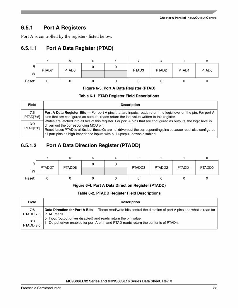
Chapter 6 Parallel Input/Output Control
MC9S08EL32 Series and MC9S08SL16 Series Data Sheet, Rev. 3
Freescale Semiconductor 83
6.5.1 Port A Registers
Port A is controlled by the registers listed below.
6.5.1.1 Port A Data Register (PTAD)
6.5.1.2 Port A Data Direction Register (PTADD)
7 6 5 4 3 2 1 0
RPTAD7 PTAD6
0 0PTAD3 PTAD2 PTAD1 PTAD0
W
Reset: 0 0 0 0 0 0 0 0
Figure 6-3. Port A Data Register (PTAD)
Table 6-1. PTAD Register Field Descriptions
Field Description
7:6PTAD[7:6]
Port A Data Register Bits — For port A pins that are inputs, reads return the logic level on the pin. For port A pins that are configured as outputs, reads return the last value written to this register.Writes are latched into all bits of this register. For port A pins that are configured as outputs, the logic level is driven out the corresponding MCU pin. Reset forces PTAD to all 0s, but these 0s are not driven out the corresponding pins because reset also configures all port pins as high-impedance inputs with pull-ups/pull-downs disabled.
3:0PTAD[3:0]
7 6 5 4 3 2 1 0
RPTADD7 PTADD6
0 0PTADD3 PTADD2 PTADD1 PTADD0
W
Reset: 0 0 0 0 0 0 0 0
Figure 6-4. Port A Data Direction Register (PTADD)
Table 6-2. PTADD Register Field Descriptions
Field Description
7:6PTADD[7:6]
Data Direction for Port A Bits — These read/write bits control the direction of port A pins and what is read for PTAD reads. 0 Input (output driver disabled) and reads return the pin value. 1 Output driver enabled for port A bit n and PTAD reads return the contents of PTADn.3:0
PTADD[3:0]
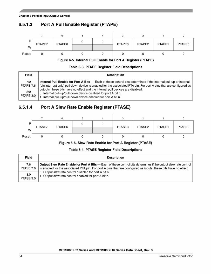
Chapter 6 Parallel Input/Output Control
MC9S08EL32 Series and MC9S08SL16 Series Data Sheet, Rev. 3
84 Freescale Semiconductor
6.5.1.3 Port A Pull Enable Register (PTAPE)
6.5.1.4 Port A Slew Rate Enable Register (PTASE)
7 6 5 4 3 2 1 0
RPTAPE7 PTAPE6
0 0PTAPE3 PTAPE2 PTAPE1 PTAPE0
W
Reset: 0 0 0 0 0 0 0 0
Figure 6-5. Internal Pull Enable for Port A Register (PTAPE)
Table 6-3. PTAPE Register Field Descriptions
Field Description
7:0PTAPE[7:6]
Internal Pull Enable for Port A Bits — Each of these control bits determines if the internal pull-up or internal (pin interrupt only) pull-down device is enabled for the associated PTA pin. For port A pins that are configured as outputs, these bits have no effect and the internal pull devices are disabled.0 Internal pull-up/pull-down device disabled for port A bit n.1 Internal pull-up/pull-down device enabled for port A bit n.
3:0PTAPE[3:0]
7 6 5 4 3 2 1 0
RPTASE7 PTASE6
0 0PTASE3 PTASE2 PTASE1 PTASE0
W
Reset: 0 0 0 0 0 0 0 0
Figure 6-6. Slew Rate Enable for Port A Register (PTASE)
Table 6-4. PTASE Register Field Descriptions
Field Description
7:6PTASE[7:6]
Output Slew Rate Enable for Port A Bits — Each of these control bits determines if the output slew rate control is enabled for the associated PTA pin. For port A pins that are configured as inputs, these bits have no effect.0 Output slew rate control disabled for port A bit n.1 Output slew rate control enabled for port A bit n.3:0
PTASE[3:0]
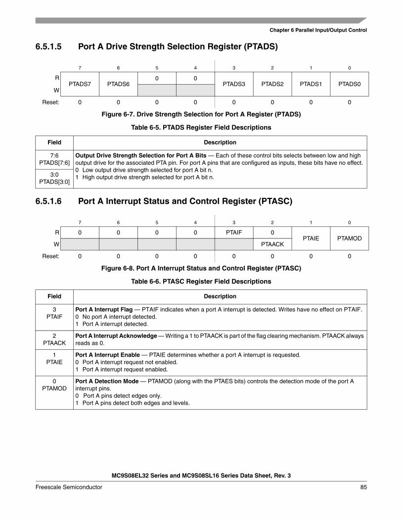
Chapter 6 Parallel Input/Output Control
MC9S08EL32 Series and MC9S08SL16 Series Data Sheet, Rev. 3
Freescale Semiconductor 85
6.5.1.5 Port A Drive Strength Selection Register (PTADS)
6.5.1.6 Port A Interrupt Status and Control Register (PTASC)
7 6 5 4 3 2 1 0
RPTADS7 PTADS6
0 0PTADS3 PTADS2 PTADS1 PTADS0
W
Reset: 0 0 0 0 0 0 0 0
Figure 6-7. Drive Strength Selection for Port A Register (PTADS)
Table 6-5. PTADS Register Field Descriptions
Field Description
7:6PTADS[7:6]
Output Drive Strength Selection for Port A Bits — Each of these control bits selects between low and high output drive for the associated PTA pin. For port A pins that are configured as inputs, these bits have no effect.0 Low output drive strength selected for port A bit n.1 High output drive strength selected for port A bit n.3:0
PTADS[3:0]
7 6 5 4 3 2 1 0
R 0 0 0 0 PTAIF 0PTAIE PTAMOD
W PTAACK
Reset: 0 0 0 0 0 0 0 0
Figure 6-8. Port A Interrupt Status and Control Register (PTASC)
Table 6-6. PTASC Register Field Descriptions
Field Description
3PTAIF
Port A Interrupt Flag — PTAIF indicates when a port A interrupt is detected. Writes have no effect on PTAIF.0 No port A interrupt detected.1 Port A interrupt detected.
2PTAACK
Port A Interrupt Acknowledge — Writing a 1 to PTAACK is part of the flag clearing mechanism. PTAACK always reads as 0.
1PTAIE
Port A Interrupt Enable — PTAIE determines whether a port A interrupt is requested.0 Port A interrupt request not enabled.1 Port A interrupt request enabled.
0PTAMOD
Port A Detection Mode — PTAMOD (along with the PTAES bits) controls the detection mode of the port A interrupt pins.0 Port A pins detect edges only.1 Port A pins detect both edges and levels.

Chapter 6 Parallel Input/Output Control
MC9S08EL32 Series and MC9S08SL16 Series Data Sheet, Rev. 3
86 Freescale Semiconductor
6.5.1.7 Port A Interrupt Pin Select Register (PTAPS)
6.5.1.8 Port A Interrupt Edge Select Register (PTAES)
7 6 5 4 3 2 1 0
R 0 0 0 0PTAPS3 PTAPS2 PTAPS1 PTAPS0
W
Reset: 0 0 0 0 0 0 0 0
Figure 6-9. Port A Interrupt Pin Select Register (PTAPS)
Table 6-7. PTAPS Register Field Descriptions
Field Description
3:0PTAPS[3:0]
Port A Interrupt Pin Selects — Each of the PTAPSn bits enable the corresponding port A interrupt pin.0 Pin not enabled as interrupt.1 Pin enabled as interrupt.
7 6 5 4 3 2 1 0
R 0 0 0 0PTAES3 PTAES2 PTAES1 PTAES0
W
Reset: 0 0 0 0 0 0 0 0
Figure 6-10. Port A Edge Select Register (PTAES)
Table 6-8. PTAES Register Field Descriptions
Field Description
3:0PTAES[3:0]
Port A Edge Selects — Each of the PTAESn bits serves a dual purpose by selecting the polarity of the active interrupt edge as well as selecting a pull-up or pull-down device if enabled.0 A pull-up device is connected to the associated pin interrupt and detects falling edge/low level for interrupt
generation.1 A pull-down device is connected to the associated pin interrupt and detects rising edge/high level for interrupt
generation.

Chapter 6 Parallel Input/Output Control
MC9S08EL32 Series and MC9S08SL16 Series Data Sheet, Rev. 3
Freescale Semiconductor 87
6.5.2 Port B Registers
Port B is controlled by the registers listed below.
6.5.2.1 Port B Data Register (PTBD)
6.5.2.2 Port B Data Direction Register (PTBDD)
7 6 5 4 3 2 1 0
RPTBD7 PTBD6 PTBD5 PTBD4 PTBD3 PTBD2 PTBD1 PTBD0
W
Reset: 0 0 0 0 0 0 0 0
Figure 6-11. Port B Data Register (PTBD)
Table 6-9. PTBD Register Field Descriptions
Field Description
7:0PTBD[7:0]
Port B Data Register Bits — For port B pins that are inputs, reads return the logic level on the pin. For port B pins that are configured as outputs, reads return the last value written to this register.Writes are latched into all bits of this register. For port B pins that are configured as outputs, the logic level is driven out the corresponding MCU pin. Reset forces PTBD to all 0s, but these 0s are not driven out the corresponding pins because reset also configures all port pins as high-impedance inputs with pull-ups/pull-downs disabled.
7 6 5 4 3 2 1 0
RPTBDD7 PTBDD6 PTBDD5 PTBDD4 PTBDD3 PTBDD2 PTBDD1 PTBDD0
W
Reset: 0 0 0 0 0 0 0 0
Figure 6-12. Port B Data Direction Register (PTBDD)
Table 6-10. PTBDD Register Field Descriptions
Field Description
7:0PTBDD[7:0]
Data Direction for Port B Bits — These read/write bits control the direction of port B pins and what is read for PTBD reads. 0 Input (output driver disabled) and reads return the pin value. 1 Output driver enabled for port B bit n and PTBD reads return the contents of PTBDn.
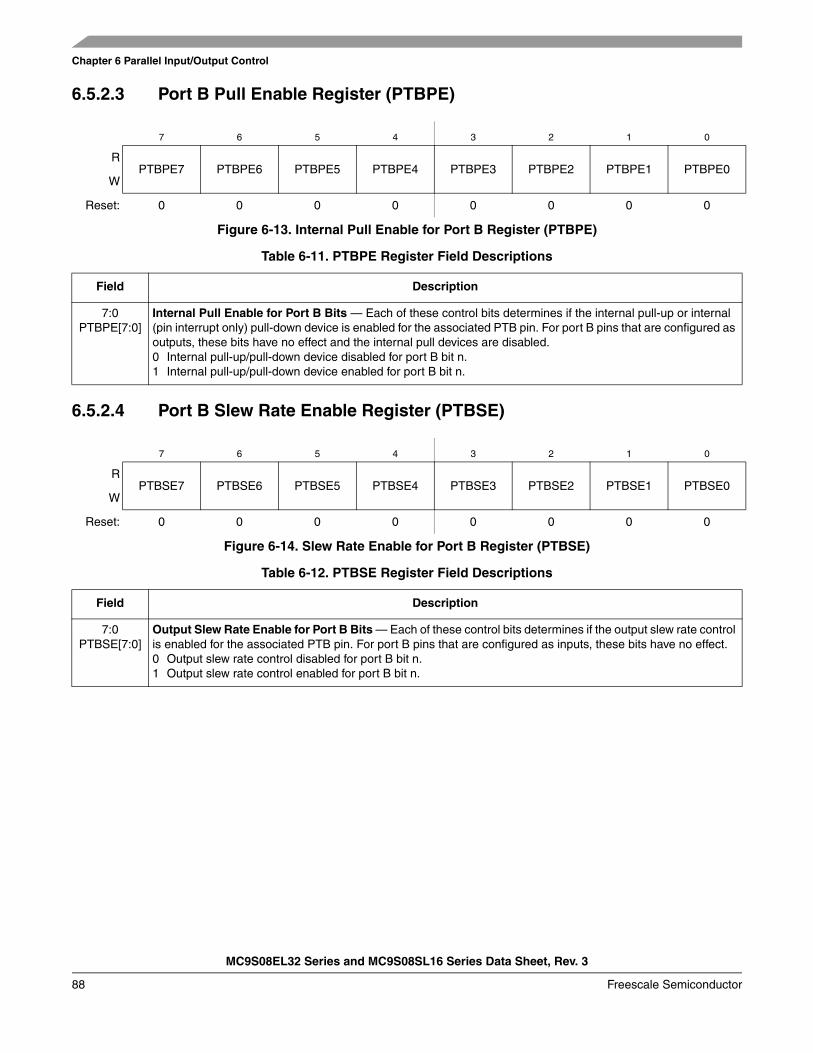
Chapter 6 Parallel Input/Output Control
MC9S08EL32 Series and MC9S08SL16 Series Data Sheet, Rev. 3
88 Freescale Semiconductor
6.5.2.3 Port B Pull Enable Register (PTBPE)
6.5.2.4 Port B Slew Rate Enable Register (PTBSE)
7 6 5 4 3 2 1 0
RPTBPE7 PTBPE6 PTBPE5 PTBPE4 PTBPE3 PTBPE2 PTBPE1 PTBPE0
W
Reset: 0 0 0 0 0 0 0 0
Figure 6-13. Internal Pull Enable for Port B Register (PTBPE)
Table 6-11. PTBPE Register Field Descriptions
Field Description
7:0PTBPE[7:0]
Internal Pull Enable for Port B Bits — Each of these control bits determines if the internal pull-up or internal (pin interrupt only) pull-down device is enabled for the associated PTB pin. For port B pins that are configured as outputs, these bits have no effect and the internal pull devices are disabled.0 Internal pull-up/pull-down device disabled for port B bit n.1 Internal pull-up/pull-down device enabled for port B bit n.
7 6 5 4 3 2 1 0
RPTBSE7 PTBSE6 PTBSE5 PTBSE4 PTBSE3 PTBSE2 PTBSE1 PTBSE0
W
Reset: 0 0 0 0 0 0 0 0
Figure 6-14. Slew Rate Enable for Port B Register (PTBSE)
Table 6-12. PTBSE Register Field Descriptions
Field Description
7:0PTBSE[7:0]
Output Slew Rate Enable for Port B Bits — Each of these control bits determines if the output slew rate control is enabled for the associated PTB pin. For port B pins that are configured as inputs, these bits have no effect.0 Output slew rate control disabled for port B bit n.1 Output slew rate control enabled for port B bit n.
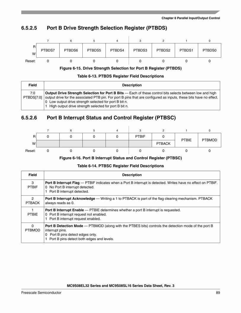
Chapter 6 Parallel Input/Output Control
MC9S08EL32 Series and MC9S08SL16 Series Data Sheet, Rev. 3
Freescale Semiconductor 89
6.5.2.5 Port B Drive Strength Selection Register (PTBDS)
6.5.2.6 Port B Interrupt Status and Control Register (PTBSC)
7 6 5 4 3 2 1 0
RPTBDS7 PTBDS6 PTBDS5 PTBDS4 PTBDS3 PTBDS2 PTBDS1 PTBDS0
W
Reset: 0 0 0 0 0 0 0 0
Figure 6-15. Drive Strength Selection for Port B Register (PTBDS)
Table 6-13. PTBDS Register Field Descriptions
Field Description
7:0PTBDS[7:0]
Output Drive Strength Selection for Port B Bits — Each of these control bits selects between low and high output drive for the associated PTB pin. For port B pins that are configured as inputs, these bits have no effect.0 Low output drive strength selected for port B bit n.1 High output drive strength selected for port B bit n.
7 6 5 4 3 2 1 0
R 0 0 0 0 PTBIF 0PTBIE PTBMOD
W PTBACK
Reset: 0 0 0 0 0 0 0 0
Figure 6-16. Port B Interrupt Status and Control Register (PTBSC)
Table 6-14. PTBSC Register Field Descriptions
Field Description
3PTBIF
Port B Interrupt Flag — PTBIF indicates when a Port B interrupt is detected. Writes have no effect on PTBIF.0 No Port B interrupt detected.1 Port B interrupt detected.
2PTBACK
Port B Interrupt Acknowledge — Writing a 1 to PTBACK is part of the flag clearing mechanism. PTBACK always reads as 0.
1PTBIE
Port B Interrupt Enable — PTBIE determines whether a port B interrupt is requested.0 Port B interrupt request not enabled.1 Port B interrupt request enabled.
0PTBMOD
Port B Detection Mode — PTBMOD (along with the PTBES bits) controls the detection mode of the port B interrupt pins.0 Port B pins detect edges only.1 Port B pins detect both edges and levels.
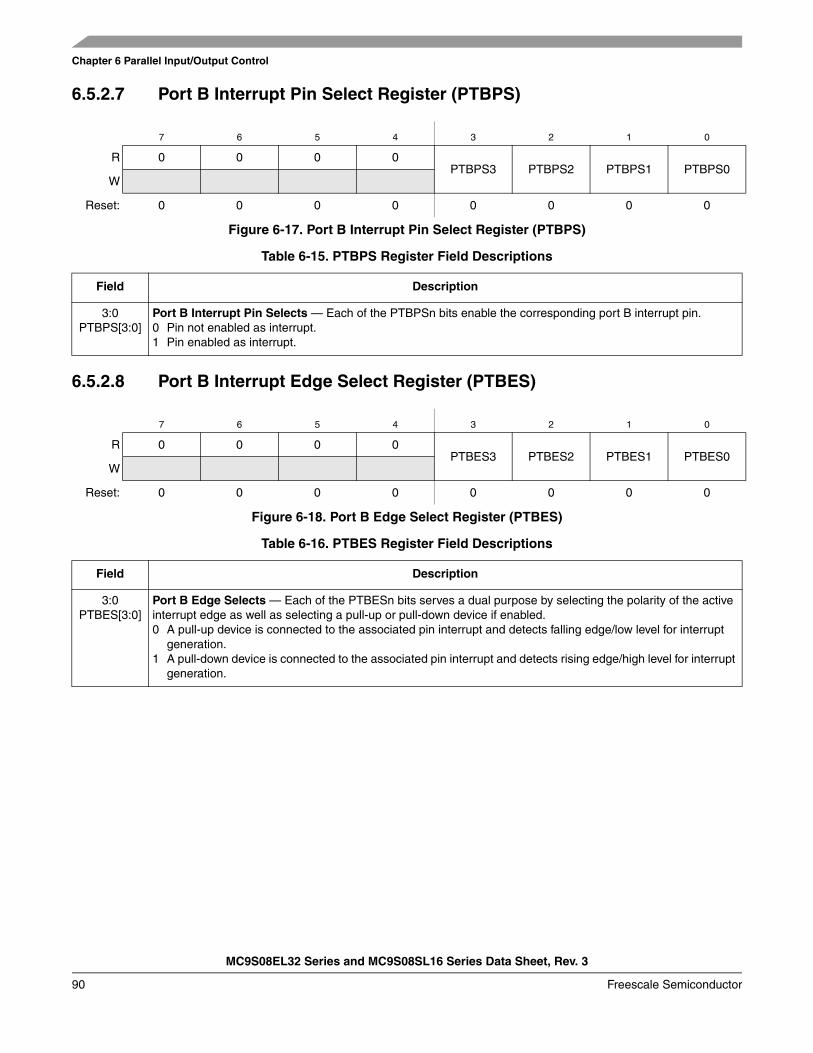
Chapter 6 Parallel Input/Output Control
MC9S08EL32 Series and MC9S08SL16 Series Data Sheet, Rev. 3
90 Freescale Semiconductor
6.5.2.7 Port B Interrupt Pin Select Register (PTBPS)
6.5.2.8 Port B Interrupt Edge Select Register (PTBES)
7 6 5 4 3 2 1 0
R 0 0 0 0PTBPS3 PTBPS2 PTBPS1 PTBPS0
W
Reset: 0 0 0 0 0 0 0 0
Figure 6-17. Port B Interrupt Pin Select Register (PTBPS)
Table 6-15. PTBPS Register Field Descriptions
Field Description
3:0PTBPS[3:0]
Port B Interrupt Pin Selects — Each of the PTBPSn bits enable the corresponding port B interrupt pin.0 Pin not enabled as interrupt.1 Pin enabled as interrupt.
7 6 5 4 3 2 1 0
R 0 0 0 0PTBES3 PTBES2 PTBES1 PTBES0
W
Reset: 0 0 0 0 0 0 0 0
Figure 6-18. Port B Edge Select Register (PTBES)
Table 6-16. PTBES Register Field Descriptions
Field Description
3:0PTBES[3:0]
Port B Edge Selects — Each of the PTBESn bits serves a dual purpose by selecting the polarity of the active interrupt edge as well as selecting a pull-up or pull-down device if enabled.0 A pull-up device is connected to the associated pin interrupt and detects falling edge/low level for interrupt
generation.1 A pull-down device is connected to the associated pin interrupt and detects rising edge/high level for interrupt
generation.
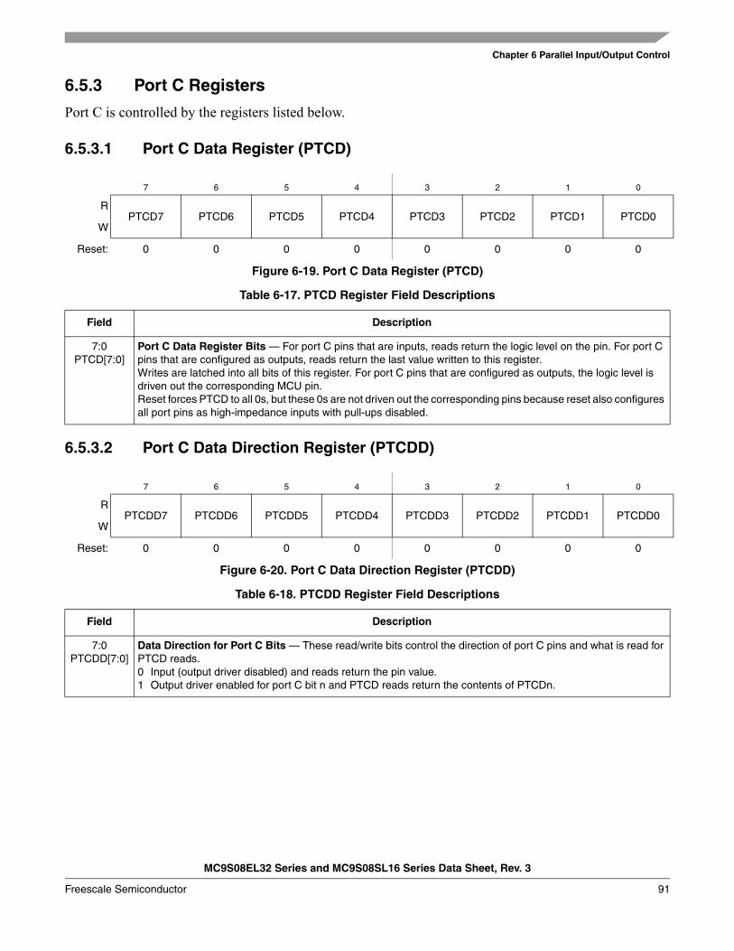
Chapter 6 Parallel Input/Output Control
MC9S08EL32 Series and MC9S08SL16 Series Data Sheet, Rev. 3
Freescale Semiconductor 91
6.5.3 Port C Registers
Port C is controlled by the registers listed below.
6.5.3.1 Port C Data Register (PTCD)
6.5.3.2 Port C Data Direction Register (PTCDD)
7 6 5 4 3 2 1 0
RPTCD7 PTCD6 PTCD5 PTCD4 PTCD3 PTCD2 PTCD1 PTCD0
W
Reset: 0 0 0 0 0 0 0 0
Figure 6-19. Port C Data Register (PTCD)
Table 6-17. PTCD Register Field Descriptions
Field Description
7:0PTCD[7:0]
Port C Data Register Bits — For port C pins that are inputs, reads return the logic level on the pin. For port C pins that are configured as outputs, reads return the last value written to this register.Writes are latched into all bits of this register. For port C pins that are configured as outputs, the logic level is driven out the corresponding MCU pin. Reset forces PTCD to all 0s, but these 0s are not driven out the corresponding pins because reset also configures all port pins as high-impedance inputs with pull-ups disabled.
7 6 5 4 3 2 1 0
RPTCDD7 PTCDD6 PTCDD5 PTCDD4 PTCDD3 PTCDD2 PTCDD1 PTCDD0
W
Reset: 0 0 0 0 0 0 0 0
Figure 6-20. Port C Data Direction Register (PTCDD)
Table 6-18. PTCDD Register Field Descriptions
Field Description
7:0PTCDD[7:0]
Data Direction for Port C Bits — These read/write bits control the direction of port C pins and what is read for PTCD reads. 0 Input (output driver disabled) and reads return the pin value. 1 Output driver enabled for port C bit n and PTCD reads return the contents of PTCDn.
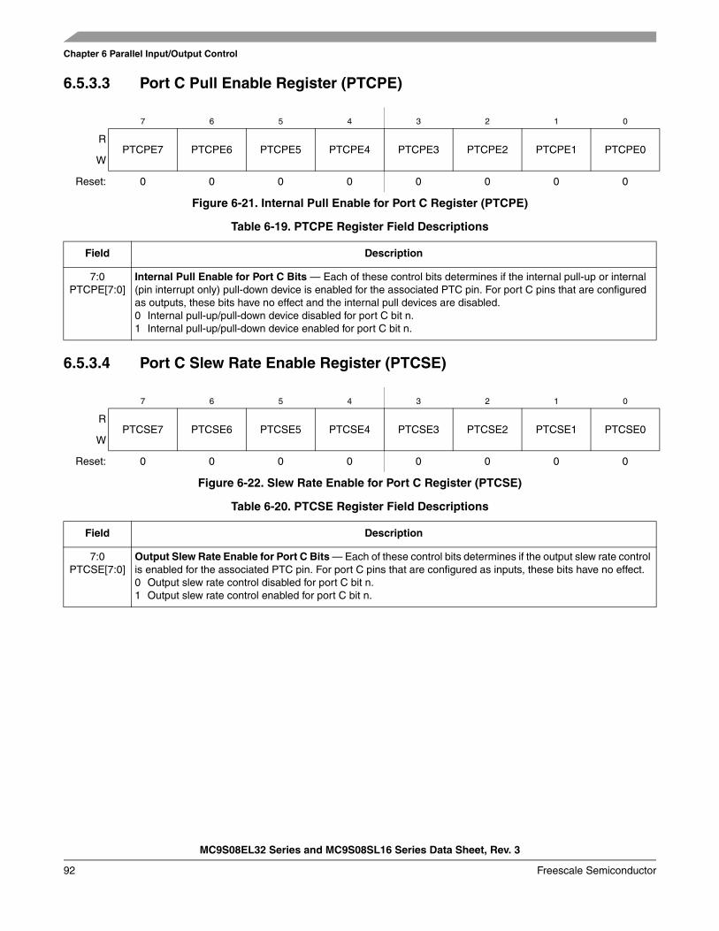
Chapter 6 Parallel Input/Output Control
MC9S08EL32 Series and MC9S08SL16 Series Data Sheet, Rev. 3
92 Freescale Semiconductor
6.5.3.3 Port C Pull Enable Register (PTCPE)
6.5.3.4 Port C Slew Rate Enable Register (PTCSE)
7 6 5 4 3 2 1 0
RPTCPE7 PTCPE6 PTCPE5 PTCPE4 PTCPE3 PTCPE2 PTCPE1 PTCPE0
W
Reset: 0 0 0 0 0 0 0 0
Figure 6-21. Internal Pull Enable for Port C Register (PTCPE)
Table 6-19. PTCPE Register Field Descriptions
Field Description
7:0PTCPE[7:0]
Internal Pull Enable for Port C Bits — Each of these control bits determines if the internal pull-up or internal (pin interrupt only) pull-down device is enabled for the associated PTC pin. For port C pins that are configured as outputs, these bits have no effect and the internal pull devices are disabled.0 Internal pull-up/pull-down device disabled for port C bit n.1 Internal pull-up/pull-down device enabled for port C bit n.
7 6 5 4 3 2 1 0
RPTCSE7 PTCSE6 PTCSE5 PTCSE4 PTCSE3 PTCSE2 PTCSE1 PTCSE0
W
Reset: 0 0 0 0 0 0 0 0
Figure 6-22. Slew Rate Enable for Port C Register (PTCSE)
Table 6-20. PTCSE Register Field Descriptions
Field Description
7:0PTCSE[7:0]
Output Slew Rate Enable for Port C Bits — Each of these control bits determines if the output slew rate control is enabled for the associated PTC pin. For port C pins that are configured as inputs, these bits have no effect.0 Output slew rate control disabled for port C bit n.1 Output slew rate control enabled for port C bit n.
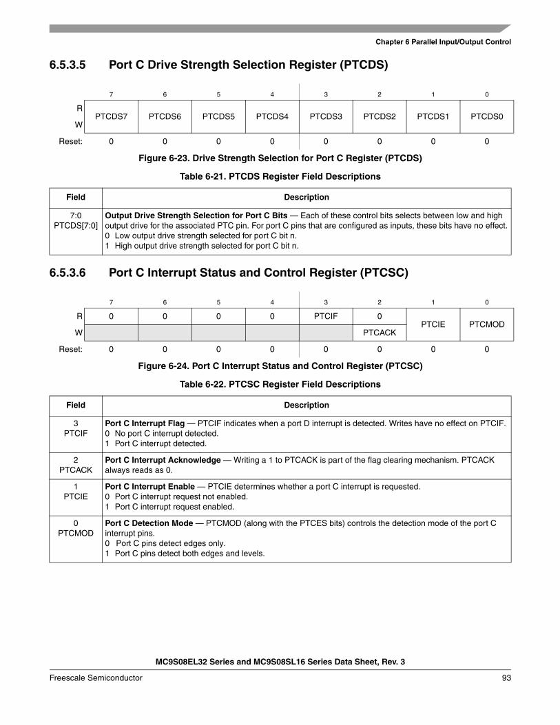
Chapter 6 Parallel Input/Output Control
MC9S08EL32 Series and MC9S08SL16 Series Data Sheet, Rev. 3
Freescale Semiconductor 93
6.5.3.5 Port C Drive Strength Selection Register (PTCDS)
6.5.3.6 Port C Interrupt Status and Control Register (PTCSC)
7 6 5 4 3 2 1 0
RPTCDS7 PTCDS6 PTCDS5 PTCDS4 PTCDS3 PTCDS2 PTCDS1 PTCDS0
W
Reset: 0 0 0 0 0 0 0 0
Figure 6-23. Drive Strength Selection for Port C Register (PTCDS)
Table 6-21. PTCDS Register Field Descriptions
Field Description
7:0PTCDS[7:0]
Output Drive Strength Selection for Port C Bits — Each of these control bits selects between low and high output drive for the associated PTC pin. For port C pins that are configured as inputs, these bits have no effect.0 Low output drive strength selected for port C bit n.1 High output drive strength selected for port C bit n.
7 6 5 4 3 2 1 0
R 0 0 0 0 PTCIF 0PTCIE PTCMOD
W PTCACK
Reset: 0 0 0 0 0 0 0 0
Figure 6-24. Port C Interrupt Status and Control Register (PTCSC)
Table 6-22. PTCSC Register Field Descriptions
Field Description
3PTCIF
Port C Interrupt Flag — PTCIF indicates when a port D interrupt is detected. Writes have no effect on PTCIF.0 No port C interrupt detected.1 Port C interrupt detected.
2PTCACK
Port C Interrupt Acknowledge — Writing a 1 to PTCACK is part of the flag clearing mechanism. PTCACK always reads as 0.
1PTCIE
Port C Interrupt Enable — PTCIE determines whether a port C interrupt is requested.0 Port C interrupt request not enabled.1 Port C interrupt request enabled.
0PTCMOD
Port C Detection Mode — PTCMOD (along with the PTCES bits) controls the detection mode of the port C interrupt pins.0 Port C pins detect edges only.1 Port C pins detect both edges and levels.
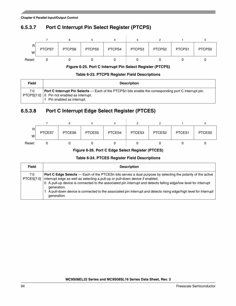
Chapter 6 Parallel Input/Output Control
MC9S08EL32 Series and MC9S08SL16 Series Data Sheet, Rev. 3
94 Freescale Semiconductor
6.5.3.7 Port C Interrupt Pin Select Register (PTCPS)
6.5.3.8 Port C Interrupt Edge Select Register (PTCES)
7 6 5 4 3 2 1 0
RPTCPS7 PTCPS6 PTCPS5 PTCPS4 PTCPS3 PTCPS2 PTCPS1 PTCPS0
W
Reset: 0 0 0 0 0 0 0 0
Figure 6-25. Port C Interrupt Pin Select Register (PTCPS)
Table 6-23. PTCPS Register Field Descriptions
Field Description
7:0PTCPS[7:0]
Port C Interrupt Pin Selects — Each of the PTCPSn bits enable the corresponding port C interrupt pin.0 Pin not enabled as interrupt.1 Pin enabled as interrupt.
7 6 5 4 3 2 1 0
RPTCES7 PTCES6 PTCES5 PTCES4 PTCES3 PTCES2 PTCES1 PTCES0
W
Reset: 0 0 0 0 0 0 0 0
Figure 6-26. Port C Edge Select Register (PTCES)
Table 6-24. PTCES Register Field Descriptions
Field Description
7:0PTCES[7:0]
Port C Edge Selects — Each of the PTCESn bits serves a dual purpose by selecting the polarity of the active interrupt edge as well as selecting a pull-up or pull-down device if enabled.0 A pull-up device is connected to the associated pin interrupt and detects falling edge/low level for interrupt
generation.1 A pull-down device is connected to the associated pin interrupt and detects rising edge/high level for interrupt
generation.
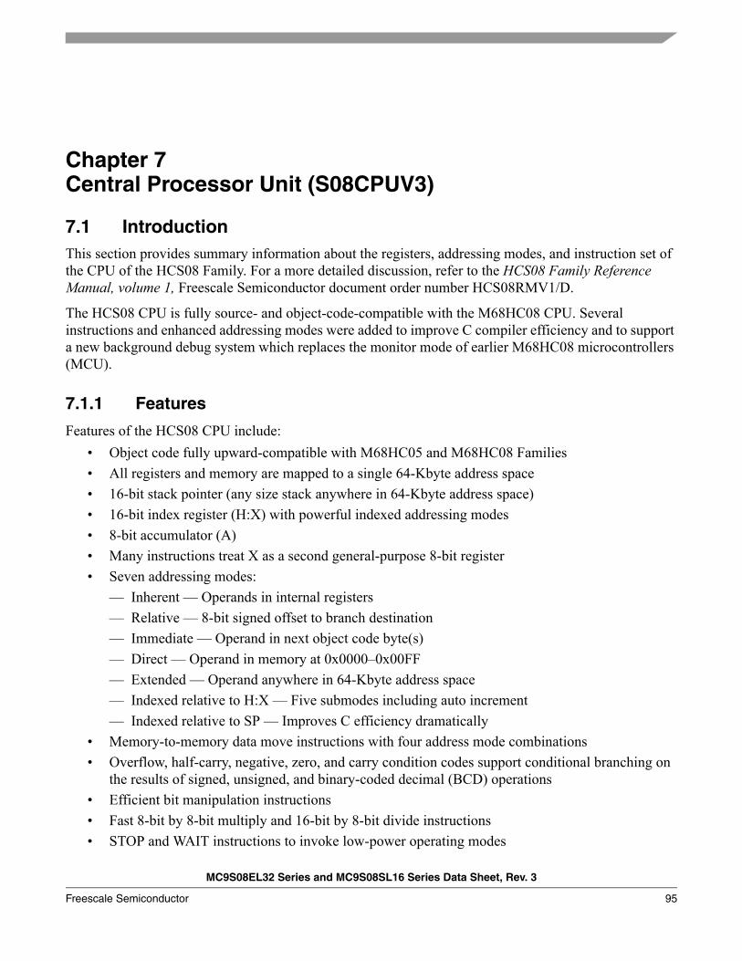
MC9S08EL32 Series and MC9S08SL16 Series Data Sheet, Rev. 3
Freescale Semiconductor 95
Chapter 7 Central Processor Unit (S08CPUV3)
7.1 IntroductionThis section provides summary information about the registers, addressing modes, and instruction set of the CPU of the HCS08 Family. For a more detailed discussion, refer to the HCS08 Family Reference Manual, volume 1, Freescale Semiconductor document order number HCS08RMV1/D.
The HCS08 CPU is fully source- and object-code-compatible with the M68HC08 CPU. Several instructions and enhanced addressing modes were added to improve C compiler efficiency and to support a new background debug system which replaces the monitor mode of earlier M68HC08 microcontrollers (MCU).
7.1.1 Features
Features of the HCS08 CPU include:• Object code fully upward-compatible with M68HC05 and M68HC08 Families• All registers and memory are mapped to a single 64-Kbyte address space• 16-bit stack pointer (any size stack anywhere in 64-Kbyte address space)• 16-bit index register (H:X) with powerful indexed addressing modes• 8-bit accumulator (A)• Many instructions treat X as a second general-purpose 8-bit register• Seven addressing modes:
— Inherent — Operands in internal registers— Relative — 8-bit signed offset to branch destination— Immediate — Operand in next object code byte(s)— Direct — Operand in memory at 0x0000–0x00FF— Extended — Operand anywhere in 64-Kbyte address space— Indexed relative to H:X — Five submodes including auto increment— Indexed relative to SP — Improves C efficiency dramatically
• Memory-to-memory data move instructions with four address mode combinations• Overflow, half-carry, negative, zero, and carry condition codes support conditional branching on
the results of signed, unsigned, and binary-coded decimal (BCD) operations• Efficient bit manipulation instructions• Fast 8-bit by 8-bit multiply and 16-bit by 8-bit divide instructions• STOP and WAIT instructions to invoke low-power operating modes
Chapter 7 Central Processor Unit (S08CPUV3)
MC9S08EL32 Series and MC9S08SL16 Series Data Sheet, Rev. 3
96 Freescale Semiconductor
7.2 Programmer’s Model and CPU RegistersFigure 7-1 shows the five CPU registers. CPU registers are not part of the memory map.
Figure 7-1. CPU Registers
7.2.1 Accumulator (A)
The A accumulator is a general-purpose 8-bit register. One operand input to the arithmetic logic unit (ALU) is connected to the accumulator and the ALU results are often stored into the A accumulator after arithmetic and logical operations. The accumulator can be loaded from memory using various addressing modes to specify the address where the loaded data comes from, or the contents of A can be stored to memory using various addressing modes to specify the address where data from A will be stored.
Reset has no effect on the contents of the A accumulator.
7.2.2 Index Register (H:X)
This 16-bit register is actually two separate 8-bit registers (H and X), which often work together as a 16-bit address pointer where H holds the upper byte of an address and X holds the lower byte of the address. All indexed addressing mode instructions use the full 16-bit value in H:X as an index reference pointer; however, for compatibility with the earlier M68HC05 Family, some instructions operate only on the low-order 8-bit half (X).
Many instructions treat X as a second general-purpose 8-bit register that can be used to hold 8-bit data values. X can be cleared, incremented, decremented, complemented, negated, shifted, or rotated. Transfer instructions allow data to be transferred from A or transferred to A where arithmetic and logical operations can then be performed.
For compatibility with the earlier M68HC05 Family, H is forced to 0x00 during reset. Reset has no effect on the contents of X.
SP
PC
CONDITION CODE REGISTER
CARRYZERO NEGATIVE INTERRUPT MASKHALF-CARRY (FROM BIT 3)TWO’S COMPLEMENT OVERFLOW
H X
0
0
0
7
15
15
7 0
ACCUMULATOR A
INDEX REGISTER (LOW)INDEX REGISTER (HIGH)
STACK POINTER
8 7
PROGRAM COUNTER
16-BIT INDEX REGISTER H:X
CCRCV 1 1 H I N Z
Chapter 7 Central Processor Unit (S08CPUV3)
MC9S08EL32 Series and MC9S08SL16 Series Data Sheet, Rev. 3
Freescale Semiconductor 97
7.2.3 Stack Pointer (SP)
This 16-bit address pointer register points at the next available location on the automatic last-in-first-out (LIFO) stack. The stack may be located anywhere in the 64-Kbyte address space that has RAM and can be any size up to the amount of available RAM. The stack is used to automatically save the return address for subroutine calls, the return address and CPU registers during interrupts, and for local variables. The AIS (add immediate to stack pointer) instruction adds an 8-bit signed immediate value to SP. This is most often used to allocate or deallocate space for local variables on the stack.
SP is forced to 0x00FF at reset for compatibility with the earlier M68HC05 Family. HCS08 programs normally change the value in SP to the address of the last location (highest address) in on-chip RAM during reset initialization to free up direct page RAM (from the end of the on-chip registers to 0x00FF).
The RSP (reset stack pointer) instruction was included for compatibility with the M68HC05 Family and is seldom used in new HCS08 programs because it only affects the low-order half of the stack pointer.
7.2.4 Program Counter (PC)
The program counter is a 16-bit register that contains the address of the next instruction or operand to be fetched.
During normal program execution, the program counter automatically increments to the next sequential memory location every time an instruction or operand is fetched. Jump, branch, interrupt, and return operations load the program counter with an address other than that of the next sequential location. This is called a change-of-flow.
During reset, the program counter is loaded with the reset vector that is located at 0xFFFE and 0xFFFF. The vector stored there is the address of the first instruction that will be executed after exiting the reset state.
7.2.5 Condition Code Register (CCR)
The 8-bit condition code register contains the interrupt mask (I) and five flags that indicate the results of the instruction just executed. Bits 6 and 5 are set permanently to 1. The following paragraphs describe the functions of the condition code bits in general terms. For a more detailed explanation of how each instruction sets the CCR bits, refer to the HCS08 Family Reference Manual, volume 1, Freescale Semiconductor document order number HCS08RMv1.
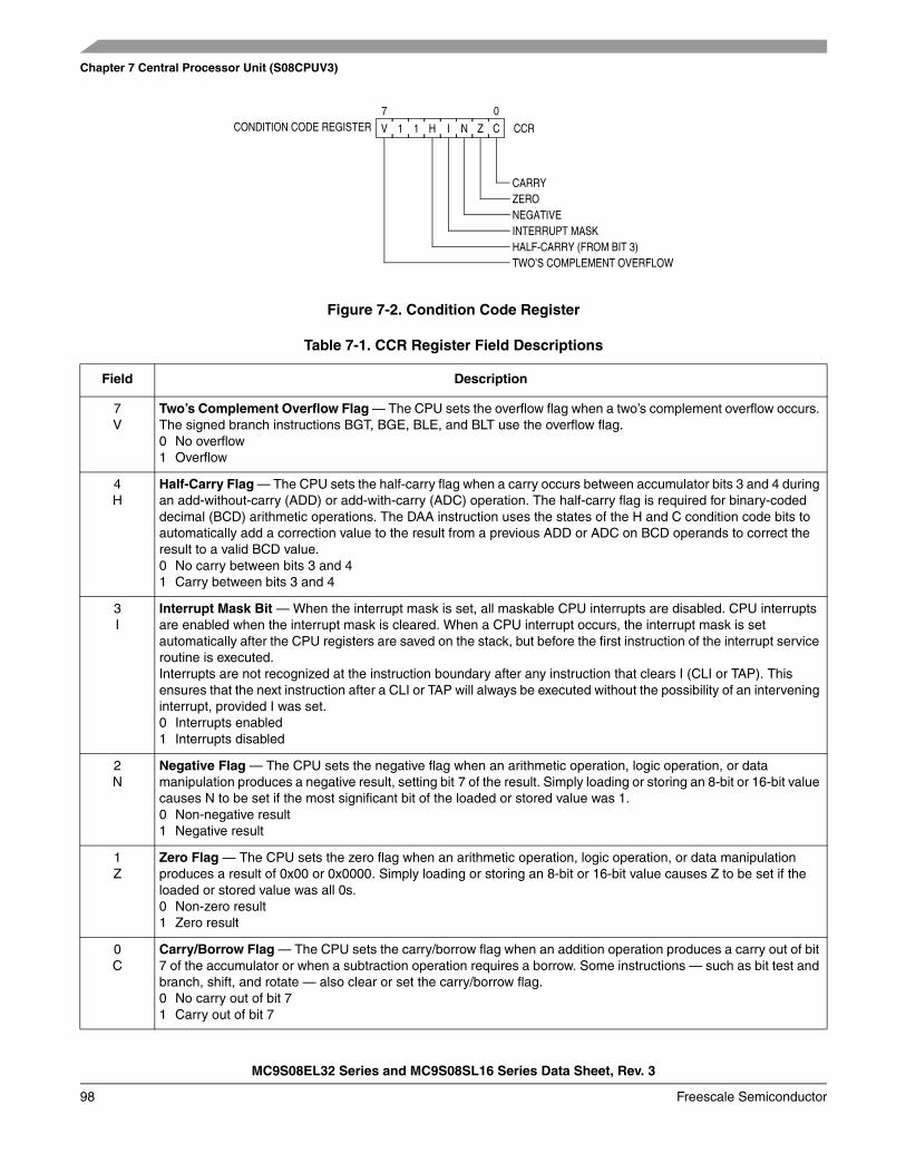
Chapter 7 Central Processor Unit (S08CPUV3)
MC9S08EL32 Series and MC9S08SL16 Series Data Sheet, Rev. 3
98 Freescale Semiconductor
Figure 7-2. Condition Code Register
Table 7-1. CCR Register Field Descriptions
Field Description
7V
Two’s Complement Overflow Flag — The CPU sets the overflow flag when a two’s complement overflow occurs. The signed branch instructions BGT, BGE, BLE, and BLT use the overflow flag.0 No overflow1 Overflow
4H
Half-Carry Flag — The CPU sets the half-carry flag when a carry occurs between accumulator bits 3 and 4 during an add-without-carry (ADD) or add-with-carry (ADC) operation. The half-carry flag is required for binary-coded decimal (BCD) arithmetic operations. The DAA instruction uses the states of the H and C condition code bits to automatically add a correction value to the result from a previous ADD or ADC on BCD operands to correct the result to a valid BCD value.0 No carry between bits 3 and 41 Carry between bits 3 and 4
3I
Interrupt Mask Bit — When the interrupt mask is set, all maskable CPU interrupts are disabled. CPU interrupts are enabled when the interrupt mask is cleared. When a CPU interrupt occurs, the interrupt mask is set automatically after the CPU registers are saved on the stack, but before the first instruction of the interrupt service routine is executed.Interrupts are not recognized at the instruction boundary after any instruction that clears I (CLI or TAP). This ensures that the next instruction after a CLI or TAP will always be executed without the possibility of an intervening interrupt, provided I was set. 0 Interrupts enabled1 Interrupts disabled
2N
Negative Flag — The CPU sets the negative flag when an arithmetic operation, logic operation, or data manipulation produces a negative result, setting bit 7 of the result. Simply loading or storing an 8-bit or 16-bit value causes N to be set if the most significant bit of the loaded or stored value was 1.0 Non-negative result1 Negative result
1Z
Zero Flag — The CPU sets the zero flag when an arithmetic operation, logic operation, or data manipulation produces a result of 0x00 or 0x0000. Simply loading or storing an 8-bit or 16-bit value causes Z to be set if the loaded or stored value was all 0s.0 Non-zero result1 Zero result
0C
Carry/Borrow Flag — The CPU sets the carry/borrow flag when an addition operation produces a carry out of bit 7 of the accumulator or when a subtraction operation requires a borrow. Some instructions — such as bit test and branch, shift, and rotate — also clear or set the carry/borrow flag.0 No carry out of bit 71 Carry out of bit 7
CONDITION CODE REGISTER
CARRYZERO NEGATIVE INTERRUPT MASKHALF-CARRY (FROM BIT 3)TWO’S COMPLEMENT OVERFLOW
7 0
CCRCV 1 1 H I N Z
Chapter 7 Central Processor Unit (S08CPUV3)
MC9S08EL32 Series and MC9S08SL16 Series Data Sheet, Rev. 3
Freescale Semiconductor 99
7.3 Addressing ModesAddressing modes define the way the CPU accesses operands and data. In the HCS08, all memory, status and control registers, and input/output (I/O) ports share a single 64-Kbyte linear address space so a 16-bit binary address can uniquely identify any memory location. This arrangement means that the same instructions that access variables in RAM can also be used to access I/O and control registers or nonvolatile program space.
Some instructions use more than one addressing mode. For instance, move instructions use one addressing mode to specify the source operand and a second addressing mode to specify the destination address. Instructions such as BRCLR, BRSET, CBEQ, and DBNZ use one addressing mode to specify the location of an operand for a test and then use relative addressing mode to specify the branch destination address when the tested condition is true. For BRCLR, BRSET, CBEQ, and DBNZ, the addressing mode listed in the instruction set tables is the addressing mode needed to access the operand to be tested, and relative addressing mode is implied for the branch destination.
7.3.1 Inherent Addressing Mode (INH)
In this addressing mode, operands needed to complete the instruction (if any) are located within CPU registers so the CPU does not need to access memory to get any operands.
7.3.2 Relative Addressing Mode (REL)
Relative addressing mode is used to specify the destination location for branch instructions. A signed 8-bit offset value is located in the memory location immediately following the opcode. During execution, if the branch condition is true, the signed offset is sign-extended to a 16-bit value and is added to the current contents of the program counter, which causes program execution to continue at the branch destination address.
7.3.3 Immediate Addressing Mode (IMM)
In immediate addressing mode, the operand needed to complete the instruction is included in the object code immediately following the instruction opcode in memory. In the case of a 16-bit immediate operand, the high-order byte is located in the next memory location after the opcode, and the low-order byte is located in the next memory location after that.
7.3.4 Direct Addressing Mode (DIR)
In direct addressing mode, the instruction includes the low-order eight bits of an address in the direct page (0x0000–0x00FF). During execution a 16-bit address is formed by concatenating an implied 0x00 for the high-order half of the address and the direct address from the instruction to get the 16-bit address where the desired operand is located. This is faster and more memory efficient than specifying a complete 16-bit address for the operand.
Chapter 7 Central Processor Unit (S08CPUV3)
MC9S08EL32 Series and MC9S08SL16 Series Data Sheet, Rev. 3
100 Freescale Semiconductor
7.3.5 Extended Addressing Mode (EXT)
In extended addressing mode, the full 16-bit address of the operand is located in the next two bytes of program memory after the opcode (high byte first).
7.3.6 Indexed Addressing Mode
Indexed addressing mode has seven variations including five that use the 16-bit H:X index register pair and two that use the stack pointer as the base reference.
7.3.6.1 Indexed, No Offset (IX)
This variation of indexed addressing uses the 16-bit value in the H:X index register pair as the address of the operand needed to complete the instruction.
7.3.6.2 Indexed, No Offset with Post Increment (IX+)
This variation of indexed addressing uses the 16-bit value in the H:X index register pair as the address of the operand needed to complete the instruction. The index register pair is then incremented (H:X = H:X + 0x0001) after the operand has been fetched. This addressing mode is only used for MOV and CBEQ instructions.
7.3.6.3 Indexed, 8-Bit Offset (IX1)
This variation of indexed addressing uses the 16-bit value in the H:X index register pair plus an unsigned 8-bit offset included in the instruction as the address of the operand needed to complete the instruction.
7.3.6.4 Indexed, 8-Bit Offset with Post Increment (IX1+)
This variation of indexed addressing uses the 16-bit value in the H:X index register pair plus an unsigned 8-bit offset included in the instruction as the address of the operand needed to complete the instruction. The index register pair is then incremented (H:X = H:X + 0x0001) after the operand has been fetched. This addressing mode is used only for the CBEQ instruction.
7.3.6.5 Indexed, 16-Bit Offset (IX2)
This variation of indexed addressing uses the 16-bit value in the H:X index register pair plus a 16-bit offset included in the instruction as the address of the operand needed to complete the instruction.
7.3.6.6 SP-Relative, 8-Bit Offset (SP1)
This variation of indexed addressing uses the 16-bit value in the stack pointer (SP) plus an unsigned 8-bit offset included in the instruction as the address of the operand needed to complete the instruction.
Chapter 7 Central Processor Unit (S08CPUV3)
MC9S08EL32 Series and MC9S08SL16 Series Data Sheet, Rev. 3
Freescale Semiconductor 101
7.3.6.7 SP-Relative, 16-Bit Offset (SP2)
This variation of indexed addressing uses the 16-bit value in the stack pointer (SP) plus a 16-bit offset included in the instruction as the address of the operand needed to complete the instruction.
7.4 Special OperationsThe CPU performs a few special operations that are similar to instructions but do not have opcodes like other CPU instructions. In addition, a few instructions such as STOP and WAIT directly affect other MCU circuitry. This section provides additional information about these operations.
7.4.1 Reset Sequence
Reset can be caused by a power-on-reset (POR) event, internal conditions such as the COP (computer operating properly) watchdog, or by assertion of an external active-low reset pin. When a reset event occurs, the CPU immediately stops whatever it is doing (the MCU does not wait for an instruction boundary before responding to a reset event). For a more detailed discussion about how the MCU recognizes resets and determines the source, refer to the Resets, Interrupts, and System Configuration chapter.
The reset event is considered concluded when the sequence to determine whether the reset came from an internal source is done and when the reset pin is no longer asserted. At the conclusion of a reset event, the CPU performs a 6-cycle sequence to fetch the reset vector from 0xFFFE and 0xFFFF and to fill the instruction queue in preparation for execution of the first program instruction.
7.4.2 Interrupt Sequence
When an interrupt is requested, the CPU completes the current instruction before responding to the interrupt. At this point, the program counter is pointing at the start of the next instruction, which is where the CPU should return after servicing the interrupt. The CPU responds to an interrupt by performing the same sequence of operations as for a software interrupt (SWI) instruction, except the address used for the vector fetch is determined by the highest priority interrupt that is pending when the interrupt sequence started.
The CPU sequence for an interrupt is: 1. Store the contents of PCL, PCH, X, A, and CCR on the stack, in that order.2. Set the I bit in the CCR.3. Fetch the high-order half of the interrupt vector.4. Fetch the low-order half of the interrupt vector.5. Delay for one free bus cycle.6. Fetch three bytes of program information starting at the address indicated by the interrupt vector
to fill the instruction queue in preparation for execution of the first instruction in the interrupt service routine.
After the CCR contents are pushed onto the stack, the I bit in the CCR is set to prevent other interrupts while in the interrupt service routine. Although it is possible to clear the I bit with an instruction in the
Chapter 7 Central Processor Unit (S08CPUV3)
MC9S08EL32 Series and MC9S08SL16 Series Data Sheet, Rev. 3
102 Freescale Semiconductor
interrupt service routine, this would allow nesting of interrupts (which is not recommended because it leads to programs that are difficult to debug and maintain).
For compatibility with the earlier M68HC05 MCUs, the high-order half of the H:X index register pair (H) is not saved on the stack as part of the interrupt sequence. The user must use a PSHH instruction at the beginning of the service routine to save H and then use a PULH instruction just before the RTI that ends the interrupt service routine. It is not necessary to save H if you are certain that the interrupt service routine does not use any instructions or auto-increment addressing modes that might change the value of H.
The software interrupt (SWI) instruction is like a hardware interrupt except that it is not masked by the global I bit in the CCR and it is associated with an instruction opcode within the program so it is not asynchronous to program execution.
7.4.3 Wait Mode Operation
The WAIT instruction enables interrupts by clearing the I bit in the CCR. It then halts the clocks to the CPU to reduce overall power consumption while the CPU is waiting for the interrupt or reset event that will wake the CPU from wait mode. When an interrupt or reset event occurs, the CPU clocks will resume and the interrupt or reset event will be processed normally.
If a serial BACKGROUND command is issued to the MCU through the background debug interface while the CPU is in wait mode, CPU clocks will resume and the CPU will enter active background mode where other serial background commands can be processed. This ensures that a host development system can still gain access to a target MCU even if it is in wait mode.
7.4.4 Stop Mode Operation
Usually, all system clocks, including the crystal oscillator (when used), are halted during stop mode to minimize power consumption. In such systems, external circuitry is needed to control the time spent in stop mode and to issue a signal to wake up the target MCU when it is time to resume processing. Unlike the earlier M68HC05 and M68HC08 MCUs, the HCS08 can be configured to keep a minimum set of clocks running in stop mode. This optionally allows an internal periodic signal to wake the target MCU from stop mode.
When a host debug system is connected to the background debug pin (BKGD) and the ENBDM control bit has been set by a serial command through the background interface (or because the MCU was reset into active background mode), the oscillator is forced to remain active when the MCU enters stop mode. In this case, if a serial BACKGROUND command is issued to the MCU through the background debug interface while the CPU is in stop mode, CPU clocks will resume and the CPU will enter active background mode where other serial background commands can be processed. This ensures that a host development system can still gain access to a target MCU even if it is in stop mode.
Recovery from stop mode depends on the particular HCS08 and whether the oscillator was stopped in stop mode. Refer to the Modes of Operation chapter for more details.
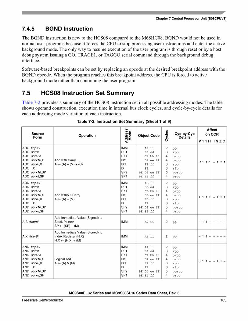
Chapter 7 Central Processor Unit (S08CPUV3)
MC9S08EL32 Series and MC9S08SL16 Series Data Sheet, Rev. 3
Freescale Semiconductor 103
7.4.5 BGND Instruction
The BGND instruction is new to the HCS08 compared to the M68HC08. BGND would not be used in normal user programs because it forces the CPU to stop processing user instructions and enter the active background mode. The only way to resume execution of the user program is through reset or by a host debug system issuing a GO, TRACE1, or TAGGO serial command through the background debug interface.
Software-based breakpoints can be set by replacing an opcode at the desired breakpoint address with the BGND opcode. When the program reaches this breakpoint address, the CPU is forced to active background mode rather than continuing the user program.
7.5 HCS08 Instruction Set SummaryTable 7-2 provides a summary of the HCS08 instruction set in all possible addressing modes. The table shows operand construction, execution time in internal bus clock cycles, and cycle-by-cycle details for each addressing mode variation of each instruction.
Table 7-2. Instruction Set Summary (Sheet 1 of 9)
SourceForm Operation
Ad
dre
ssM
od
e
Object Code
Cyc
les
Cyc-by-Cyc Details
Affecton CCR
V 1 1 H I N Z C
ADC #opr8iADC opr8aADC opr16aADC oprx16,XADC oprx8,XADC ,XADC oprx16,SPADC oprx8,SP
Add with Carry A ← (A) + (M) + (C)
IMMDIREXTIX2IX1IXSP2SP1
A9B9C9D9E9F9
9E D99E E9
iiddhh llee ffff
ee ffff
23443354
pprppprppprpprpprfppprppprpp
1 1 –
ADD #opr8iADD opr8aADD opr16aADD oprx16,XADD oprx8,XADD ,XADD oprx16,SPADD oprx8,SP
Add without CarryA ← (A) + (M)
IMMDIREXTIX2IX1IXSP2SP1
ABBBCBDBEBFB
9E DB9E EB
iiddhh llee ffff
ee ffff
23443354
pprppprppprpprpprfppprppprpp
1 1 –
AIS #opr8iAdd Immediate Value (Signed) to Stack PointerSP ← (SP) + (M)
IMM A7 ii 2 pp – 1 1 – – – – –
AIX #opr8iAdd Immediate Value (Signed) to Index Register (H:X)H:X ← (H:X) + (M)
IMM AF ii 2 pp – 1 1 – – – – –
AND #opr8iAND opr8aAND opr16aAND oprx16,XAND oprx8,XAND ,XAND oprx16,SPAND oprx8,SP
Logical AND A ← (A) & (M)
IMMDIREXTIX2IX1IXSP2SP1
A4B4C4D4E4F4
9E D49E E4
iiddhh llee ffff
ee ffff
23443354
pprppprppprpprpprfppprppprpp
0 1 1 – – –
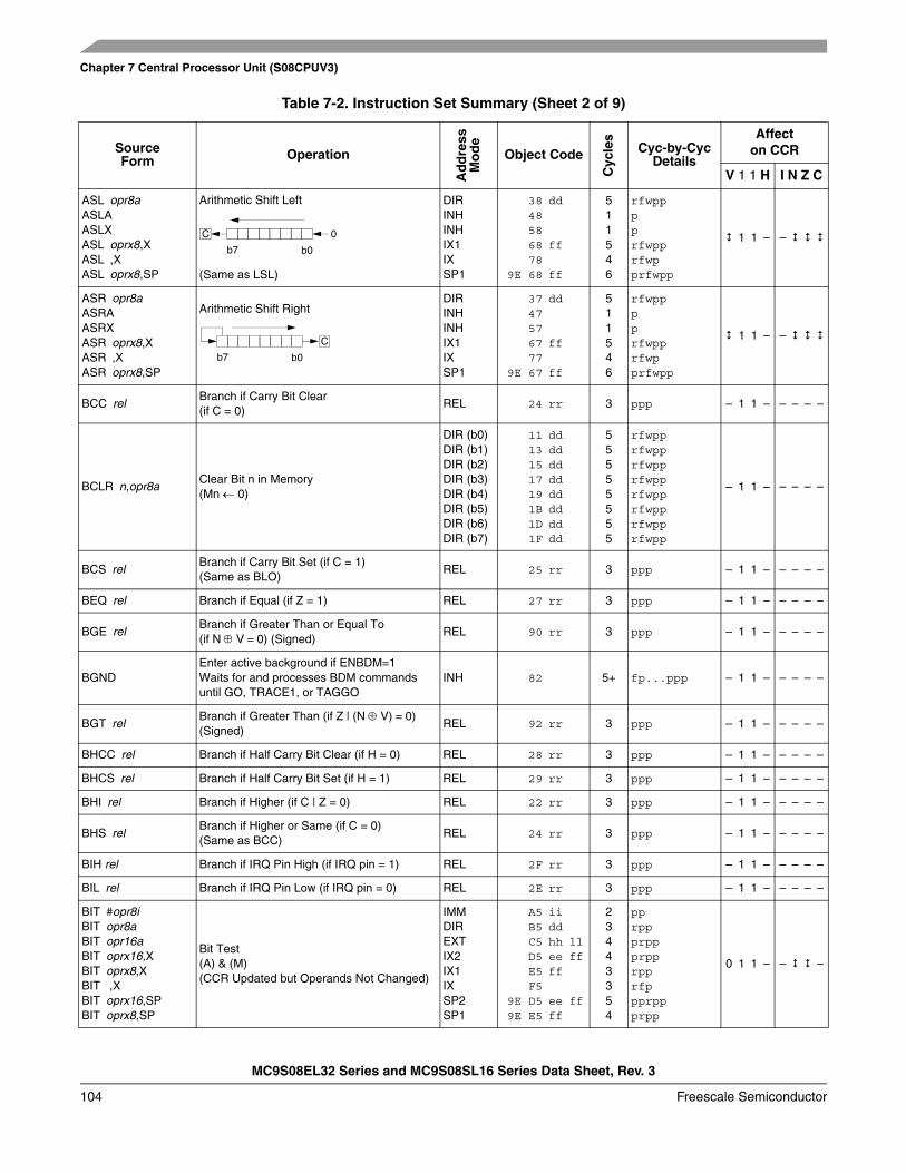
Chapter 7 Central Processor Unit (S08CPUV3)
MC9S08EL32 Series and MC9S08SL16 Series Data Sheet, Rev. 3
104 Freescale Semiconductor
ASL opr8aASLAASLXASL oprx8,XASL ,XASL oprx8,SP
Arithmetic Shift Left
(Same as LSL)
DIRINHINHIX1IXSP1
3848586878
9E 68
dd
ff
ff
511546
rfwpppprfwpprfwpprfwpp
1 1 – –
ASR opr8aASRAASRXASR oprx8,XASR ,XASR oprx8,SP
Arithmetic Shift RightDIRINHINHIX1IXSP1
3747576777
9E 67
dd
ff
ff
511546
rfwpppprfwpprfwpprfwpp
1 1 – –
BCC relBranch if Carry Bit Clear(if C = 0)
REL 24 rr 3 ppp – 1 1 – – – – –
BCLR n,opr8aClear Bit n in Memory(Mn ← 0)
DIR (b0)DIR (b1)DIR (b2)DIR (b3)DIR (b4)DIR (b5)DIR (b6)DIR (b7)
11131517191B1D1F
dddddddddddddddd
55555555
rfwpprfwpprfwpprfwpprfwpprfwpprfwpprfwpp
– 1 1 – – – – –
BCS relBranch if Carry Bit Set (if C = 1)(Same as BLO)
REL 25 rr 3 ppp – 1 1 – – – – –
BEQ rel Branch if Equal (if Z = 1) REL 27 rr 3 ppp – 1 1 – – – – –
BGE relBranch if Greater Than or Equal To (if N ⊕ V = 0) (Signed)
REL 90 rr 3 ppp – 1 1 – – – – –
BGNDEnter active background if ENBDM=1Waits for and processes BDM commands until GO, TRACE1, or TAGGO
INH 82 5+ fp...ppp – 1 1 – – – – –
BGT relBranch if Greater Than (if Z | (N ⊕ V) = 0) (Signed)
REL 92 rr 3 ppp – 1 1 – – – – –
BHCC rel Branch if Half Carry Bit Clear (if H = 0) REL 28 rr 3 ppp – 1 1 – – – – –
BHCS rel Branch if Half Carry Bit Set (if H = 1) REL 29 rr 3 ppp – 1 1 – – – – –
BHI rel Branch if Higher (if C | Z = 0) REL 22 rr 3 ppp – 1 1 – – – – –
BHS relBranch if Higher or Same (if C = 0) (Same as BCC)
REL 24 rr 3 ppp – 1 1 – – – – –
BIH rel Branch if IRQ Pin High (if IRQ pin = 1) REL 2F rr 3 ppp – 1 1 – – – – –
BIL rel Branch if IRQ Pin Low (if IRQ pin = 0) REL 2E rr 3 ppp – 1 1 – – – – –
BIT #opr8iBIT opr8aBIT opr16aBIT oprx16,XBIT oprx8,XBIT ,XBIT oprx16,SPBIT oprx8,SP
Bit Test (A) & (M)(CCR Updated but Operands Not Changed)
IMMDIREXTIX2IX1IXSP2SP1
A5B5C5D5E5F5
9E D59E E5
iiddhh llee ffff
ee ffff
23443354
pprppprppprpprpprfppprppprpp
0 1 1 – – –
Table 7-2. Instruction Set Summary (Sheet 2 of 9)
SourceForm Operation
Ad
dre
ssM
od
e
Object Code
Cyc
les
Cyc-by-Cyc Details
Affecton CCR
V 1 1 H I N Z C
C
b0b7
0
b0b7
C
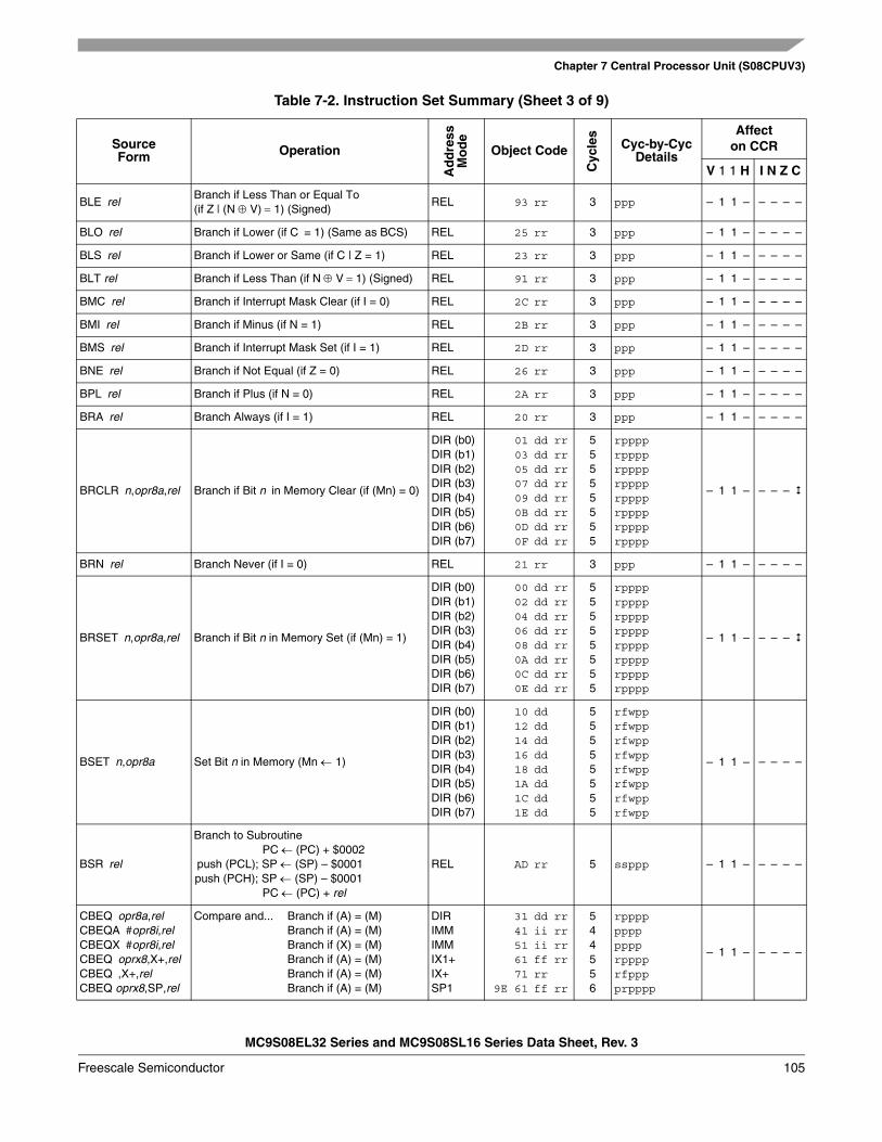
Chapter 7 Central Processor Unit (S08CPUV3)
MC9S08EL32 Series and MC9S08SL16 Series Data Sheet, Rev. 3
Freescale Semiconductor 105
BLE relBranch if Less Than or Equal To (if Z | (N ⊕ V) = 1) (Signed)
REL 93 rr 3 ppp – 1 1 – – – – –
BLO rel Branch if Lower (if C = 1) (Same as BCS) REL 25 rr 3 ppp – 1 1 – – – – –
BLS rel Branch if Lower or Same (if C | Z = 1) REL 23 rr 3 ppp – 1 1 – – – – –
BLT rel Branch if Less Than (if N ⊕ V = 1) (Signed) REL 91 rr 3 ppp – 1 1 – – – – –
BMC rel Branch if Interrupt Mask Clear (if I = 0) REL 2C rr 3 ppp – 1 1 – – – – –
BMI rel Branch if Minus (if N = 1) REL 2B rr 3 ppp – 1 1 – – – – –
BMS rel Branch if Interrupt Mask Set (if I = 1) REL 2D rr 3 ppp – 1 1 – – – – –
BNE rel Branch if Not Equal (if Z = 0) REL 26 rr 3 ppp – 1 1 – – – – –
BPL rel Branch if Plus (if N = 0) REL 2A rr 3 ppp – 1 1 – – – – –
BRA rel Branch Always (if I = 1) REL 20 rr 3 ppp – 1 1 – – – – –
BRCLR n,opr8a,rel Branch if Bit n in Memory Clear (if (Mn) = 0)
DIR (b0)DIR (b1)DIR (b2)DIR (b3)DIR (b4)DIR (b5)DIR (b6)DIR (b7)
01030507090B0D0F
dd rrdd rrdd rrdd rrdd rrdd rrdd rrdd rr
55555555
rpppprpppprpppprpppprpppprpppprpppprpppp
– 1 1 – – – –
BRN rel Branch Never (if I = 0) REL 21 rr 3 ppp – 1 1 – – – – –
BRSET n,opr8a,rel Branch if Bit n in Memory Set (if (Mn) = 1)
DIR (b0)DIR (b1)DIR (b2)DIR (b3)DIR (b4)DIR (b5)DIR (b6)DIR (b7)
00020406080A0C0E
dd rrdd rrdd rrdd rrdd rrdd rrdd rrdd rr
55555555
rpppprpppprpppprpppprpppprpppprpppprpppp
– 1 1 – – – –
BSET n,opr8a Set Bit n in Memory (Mn ← 1)
DIR (b0)DIR (b1)DIR (b2)DIR (b3)DIR (b4)DIR (b5)DIR (b6)DIR (b7)
10121416181A1C1E
dddddddddddddddd
55555555
rfwpprfwpprfwpprfwpprfwpprfwpprfwpprfwpp
– 1 1 – – – – –
BSR rel
Branch to SubroutinePC ← (PC) + $0002
push (PCL); SP ← (SP) – $0001push (PCH); SP ← (SP) – $0001
PC ← (PC) + rel
REL AD rr 5 ssppp – 1 1 – – – – –
CBEQ opr8a,relCBEQA #opr8i,relCBEQX #opr8i,relCBEQ oprx8,X+,relCBEQ ,X+,relCBEQ oprx8,SP,rel
Compare and... Branch if (A) = (M)Branch if (A) = (M)Branch if (X) = (M)Branch if (A) = (M)Branch if (A) = (M)Branch if (A) = (M)
DIRIMMIMMIX1+IX+SP1
3141516171
9E 61
dd rrii rrii rrff rrrrff rr
544556
rpppppppppppprpppprfpppprpppp
– 1 1 – – – – –
Table 7-2. Instruction Set Summary (Sheet 3 of 9)
SourceForm Operation
Ad
dre
ssM
od
e
Object Code
Cyc
les
Cyc-by-Cyc Details
Affecton CCR
V 1 1 H I N Z C
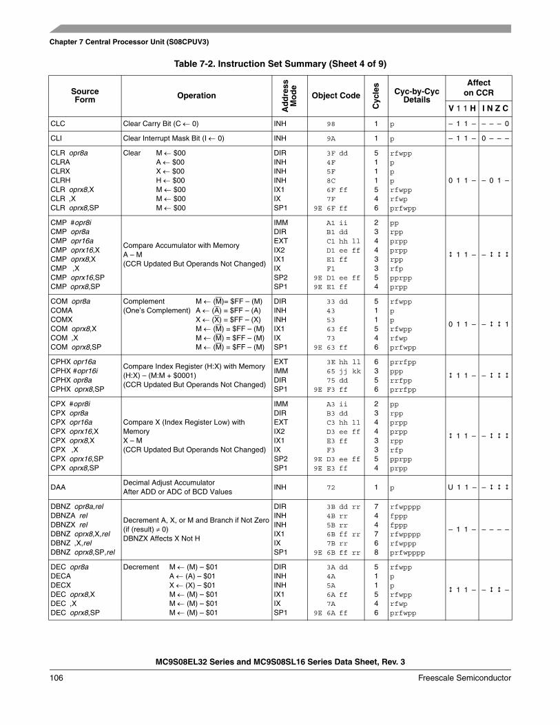
Chapter 7 Central Processor Unit (S08CPUV3)
MC9S08EL32 Series and MC9S08SL16 Series Data Sheet, Rev. 3
106 Freescale Semiconductor
CLC Clear Carry Bit (C ← 0) INH 98 1 p – 1 1 – – – – 0
CLI Clear Interrupt Mask Bit (I ← 0) INH 9A 1 p – 1 1 – 0 – – –
CLR opr8aCLRACLRXCLRHCLR oprx8,XCLR ,XCLR oprx8,SP
Clear M ← $00A ← $00X ← $00H ← $00M ← $00M ← $00M ← $00
DIRINHINHINHIX1IXSP1
3F4F5F8C6F7F
9E 6F
dd
ff
ff
5111546
rfwppppprfwpprfwpprfwpp
0 1 1 – – 0 1 –
CMP #opr8iCMP opr8aCMP opr16aCMP oprx16,XCMP oprx8,XCMP ,XCMP oprx16,SPCMP oprx8,SP
Compare Accumulator with Memory A – M(CCR Updated But Operands Not Changed)
IMMDIREXTIX2IX1IXSP2SP1
A1B1C1D1E1F1
9E D19E E1
iiddhh llee ffff
ee ffff
23443354
pprppprppprpprpprfppprppprpp
1 1 – –
COM opr8aCOMACOMXCOM oprx8,XCOM ,XCOM oprx8,SP
Complement M ← (M)= $FF – (M)(One’s Complement) A ← (A) = $FF – (A)
X ← (X) = $FF – (X)M ← (M) = $FF – (M)M ← (M) = $FF – (M)M ← (M) = $FF – (M)
DIRINHINHIX1IXSP1
3343536373
9E 63
dd
ff
ff
511546
rfwpppprfwpprfwpprfwpp
0 1 1 – – 1
CPHX opr16aCPHX #opr16iCPHX opr8aCPHX oprx8,SP
Compare Index Register (H:X) with Memory(H:X) – (M:M + $0001)(CCR Updated But Operands Not Changed)
EXTIMMDIRSP1
3E6575
9E F3
hh lljj kkddff
6356
prrfppppprrfppprrfpp
1 1 – –
CPX #opr8iCPX opr8aCPX opr16aCPX oprx16,XCPX oprx8,XCPX ,XCPX oprx16,SPCPX oprx8,SP
Compare X (Index Register Low) with Memory X – M(CCR Updated But Operands Not Changed)
IMMDIREXTIX2IX1IXSP2SP1
A3B3C3D3E3F3
9E D39E E3
iiddhh llee ffff
ee ffff
23443354
pprppprppprpprpprfppprppprpp
1 1 – –
DAADecimal Adjust Accumulator After ADD or ADC of BCD Values
INH 72 1 p U 1 1 – –
DBNZ opr8a,relDBNZA relDBNZX relDBNZ oprx8,X,relDBNZ ,X,relDBNZ oprx8,SP,rel
Decrement A, X, or M and Branch if Not Zero(if (result) ≠ 0)DBNZX Affects X Not H
DIRINHINHIX1IXSP1
3B4B5B6B7B
9E 6B
dd rrrrrrff rrrrff rr
744768
rfwppppfpppfppprfwpppprfwpppprfwpppp
– 1 1 – – – – –
DEC opr8aDECADECXDEC oprx8,XDEC ,XDEC oprx8,SP
Decrement M ← (M) – $01A ← (A) – $01X ← (X) – $01M ← (M) – $01M ← (M) – $01M ← (M) – $01
DIRINHINHIX1IXSP1
3A4A5A6A7A
9E 6A
dd
ff
ff
511546
rfwpppprfwpprfwpprfwpp
1 1 – – –
Table 7-2. Instruction Set Summary (Sheet 4 of 9)
SourceForm Operation
Ad
dre
ssM
od
e
Object Code
Cyc
les
Cyc-by-Cyc Details
Affecton CCR
V 1 1 H I N Z C
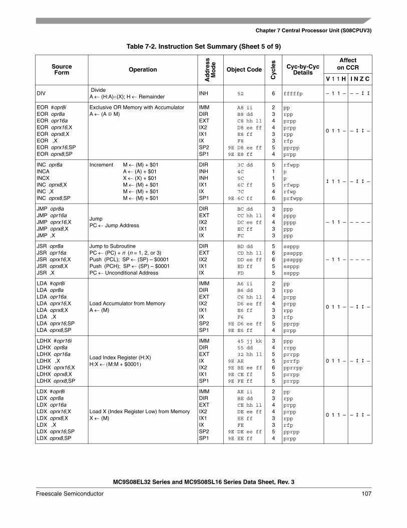
Chapter 7 Central Processor Unit (S08CPUV3)
MC9S08EL32 Series and MC9S08SL16 Series Data Sheet, Rev. 3
Freescale Semiconductor 107
DIV DivideA ← (H:A)÷(X); H ← Remainder
INH 52 6 fffffp – 1 1 – – –
EOR #opr8iEOR opr8aEOR opr16aEOR oprx16,XEOR oprx8,XEOR ,XEOR oprx16,SPEOR oprx8,SP
Exclusive OR Memory with AccumulatorA ← (A ⊕ M)
IMMDIREXTIX2IX1IXSP2SP1
A8B8C8D8E8F8
9E D89E E8
iiddhh llee ffff
ee ffff
23443354
pprppprppprpprpprfppprppprpp
0 1 1 – – –
INC opr8aINCAINCXINC oprx8,XINC ,XINC oprx8,SP
Increment M ← (M) + $01A ← (A) + $01X ← (X) + $01M ← (M) + $01M ← (M) + $01M ← (M) + $01
DIRINHINHIX1IXSP1
3C4C5C6C7C
9E 6C
dd
ff
ff
511546
rfwpppprfwpprfwpprfwpp
1 1 – – –
JMP opr8aJMP opr16aJMP oprx16,XJMP oprx8,XJMP ,X
JumpPC ← Jump Address
DIREXTIX2IX1IX
BCCCDCECFC
ddhh llee ffff
34433
ppppppppppppppppp
– 1 1 – – – – –
JSR opr8aJSR opr16aJSR oprx16,XJSR oprx8,XJSR ,X
Jump to SubroutinePC ← (PC) + n (n = 1, 2, or 3)Push (PCL); SP ← (SP) – $0001Push (PCH); SP ← (SP) – $0001PC ← Unconditional Address
DIREXTIX2IX1IX
BDCDDDEDFD
ddhh llee ffff
56655
ssppppssppppsspppsspppssppp
– 1 1 – – – – –
LDA #opr8iLDA opr8aLDA opr16aLDA oprx16,XLDA oprx8,XLDA ,XLDA oprx16,SPLDA oprx8,SP
Load Accumulator from MemoryA ← (M)
IMMDIREXTIX2IX1IXSP2SP1
A6B6C6D6E6F6
9E D69E E6
iiddhh llee ffff
ee ffff
23443354
pprppprppprpprpprfppprppprpp
0 1 1 – – –
LDHX #opr16iLDHX opr8aLDHX opr16aLDHX ,XLDHX oprx16,XLDHX oprx8,XLDHX oprx8,SP
Load Index Register (H:X) H:X ← (M:M + $0001)
IMMDIREXTIXIX2IX1SP1
455532
9E AE9E BE9E CE9E FE
jj kkddhh ll
ee ffffff
3455655
ppprrppprrppprrfppprrppprrppprrpp
0 1 1 – – –
LDX #opr8iLDX opr8aLDX opr16aLDX oprx16,XLDX oprx8,XLDX ,XLDX oprx16,SPLDX oprx8,SP
Load X (Index Register Low) from MemoryX ← (M)
IMMDIREXTIX2IX1IXSP2SP1
AEBECEDEEEFE
9E DE9E EE
iiddhh llee ffff
ee ffff
23443354
pprppprppprpprpprfppprppprpp
0 1 1 – – –
Table 7-2. Instruction Set Summary (Sheet 5 of 9)
SourceForm Operation
Ad
dre
ssM
od
e
Object Code
Cyc
les
Cyc-by-Cyc Details
Affecton CCR
V 1 1 H I N Z C
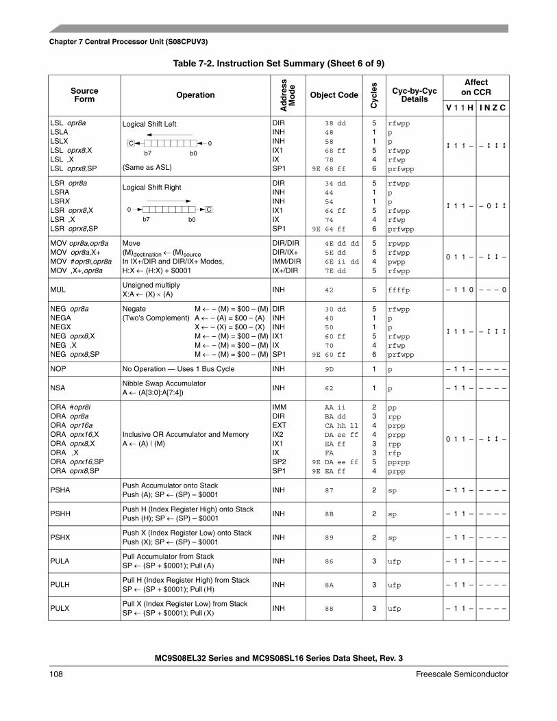
Chapter 7 Central Processor Unit (S08CPUV3)
MC9S08EL32 Series and MC9S08SL16 Series Data Sheet, Rev. 3
108 Freescale Semiconductor
LSL opr8aLSLALSLXLSL oprx8,XLSL ,XLSL oprx8,SP
Logical Shift Left
(Same as ASL)
DIRINHINHIX1IXSP1
3848586878
9E 68
dd
ff
ff
511546
rfwpppprfwpprfwpprfwpp
1 1 – –
LSR opr8aLSRALSRXLSR oprx8,XLSR ,XLSR oprx8,SP
Logical Shift RightDIRINHINHIX1IXSP1
3444546474
9E 64
dd
ff
ff
511546
rfwpppprfwpprfwpprfwpp
1 1 – – 0
MOV opr8a,opr8aMOV opr8a,X+MOV #opr8i,opr8aMOV ,X+,opr8a
Move (M)destination ← (M)sourceIn IX+/DIR and DIR/IX+ Modes, H:X ← (H:X) + $0001
DIR/DIRDIR/IX+IMM/DIRIX+/DIR
4E5E6E7E
dd ddddii dddd
5545
rpwpprfwpppwpprfwpp
0 1 1 – – –
MULUnsigned multiplyX:A ← (X) × (A)
INH 42 5 ffffp – 1 1 0 – – – 0
NEG opr8aNEGANEGXNEG oprx8,XNEG ,XNEG oprx8,SP
Negate M ← – (M) = $00 – (M)(Two’s Complement) A ← – (A) = $00 – (A)
X ← – (X) = $00 – (X)M ← – (M) = $00 – (M)M ← – (M) = $00 – (M)M ← – (M) = $00 – (M)
DIRINHINHIX1IXSP1
3040506070
9E 60
dd
ff
ff
511546
rfwpppprfwpprfwpprfwpp
1 1 – –
NOP No Operation — Uses 1 Bus Cycle INH 9D 1 p – 1 1 – – – – –
NSANibble Swap AccumulatorA ← (A[3:0]:A[7:4])
INH 62 1 p – 1 1 – – – – –
ORA #opr8iORA opr8aORA opr16aORA oprx16,XORA oprx8,XORA ,XORA oprx16,SPORA oprx8,SP
Inclusive OR Accumulator and MemoryA ← (A) | (M)
IMMDIREXTIX2IX1IXSP2SP1
AABACADAEAFA
9E DA9E EA
iiddhh llee ffff
ee ffff
23443354
pprppprppprpprpprfppprppprpp
0 1 1 – – –
PSHAPush Accumulator onto StackPush (A); SP ← (SP) – $0001
INH 87 2 sp – 1 1 – – – – –
PSHHPush H (Index Register High) onto StackPush (H); SP ← (SP) – $0001
INH 8B 2 sp – 1 1 – – – – –
PSHXPush X (Index Register Low) onto StackPush (X); SP ← (SP) – $0001
INH 89 2 sp – 1 1 – – – – –
PULAPull Accumulator from StackSP ← (SP + $0001); Pull (A)
INH 86 3 ufp – 1 1 – – – – –
PULHPull H (Index Register High) from StackSP ← (SP + $0001); Pull (H)
INH 8A 3 ufp – 1 1 – – – – –
PULXPull X (Index Register Low) from StackSP ← (SP + $0001); Pull (X)
INH 88 3 ufp – 1 1 – – – – –
Table 7-2. Instruction Set Summary (Sheet 6 of 9)
SourceForm Operation
Ad
dre
ssM
od
e
Object Code
Cyc
les
Cyc-by-Cyc Details
Affecton CCR
V 1 1 H I N Z C
C
b0b7
0
b0b7
C0
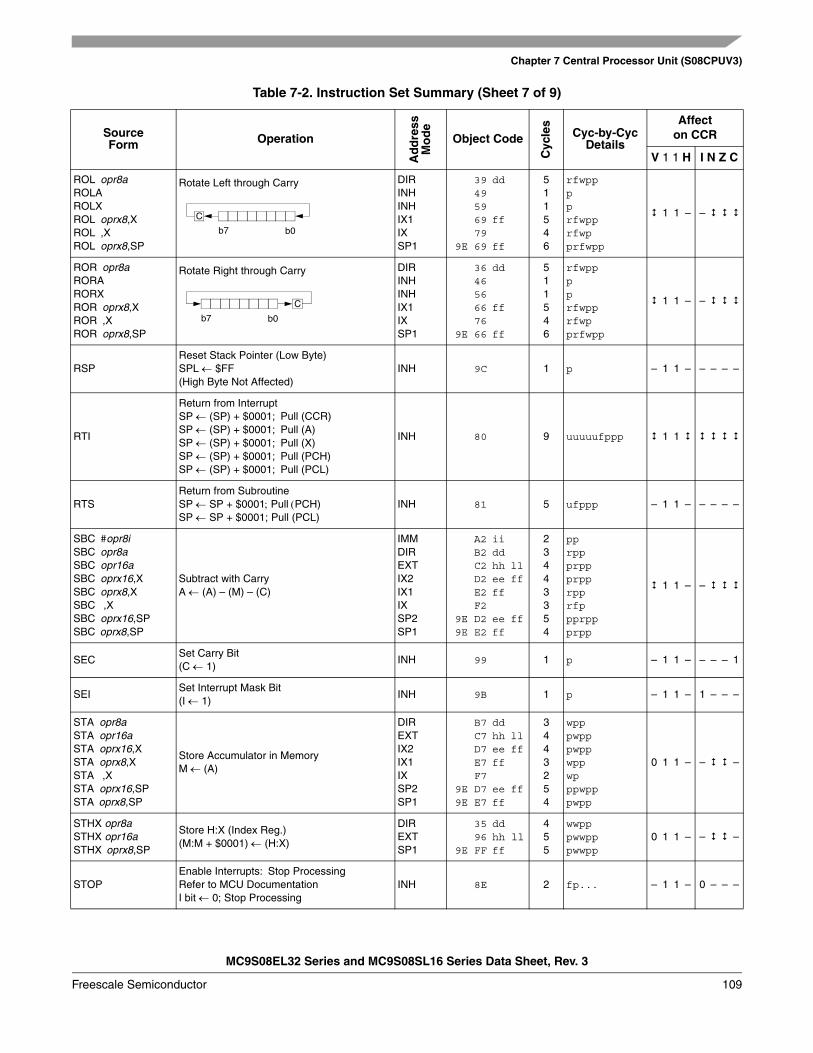
Chapter 7 Central Processor Unit (S08CPUV3)
MC9S08EL32 Series and MC9S08SL16 Series Data Sheet, Rev. 3
Freescale Semiconductor 109
ROL opr8aROLAROLXROL oprx8,XROL ,XROL oprx8,SP
Rotate Left through Carry DIRINHINHIX1IXSP1
3949596979
9E 69
dd
ff
ff
511546
rfwpppprfwpprfwpprfwpp
1 1 – –
ROR opr8aRORARORXROR oprx8,XROR ,XROR oprx8,SP
Rotate Right through Carry DIRINHINHIX1IXSP1
3646566676
9E 66
dd
ff
ff
511546
rfwpppprfwpprfwpprfwpp
1 1 – –
RSPReset Stack Pointer (Low Byte)SPL ← $FF(High Byte Not Affected)
INH 9C 1 p – 1 1 – – – – –
RTI
Return from InterruptSP ← (SP) + $0001; Pull (CCR)SP ← (SP) + $0001; Pull (A)SP ← (SP) + $0001; Pull (X)SP ← (SP) + $0001; Pull (PCH)SP ← (SP) + $0001; Pull (PCL)
INH 80 9 uuuuufppp 1 1
RTSReturn from SubroutineSP ← SP + $0001; Pull (PCH)SP ← SP + $0001; Pull (PCL)
INH 81 5 ufppp – 1 1 – – – – –
SBC #opr8iSBC opr8aSBC opr16aSBC oprx16,XSBC oprx8,XSBC ,XSBC oprx16,SPSBC oprx8,SP
Subtract with Carry A ← (A) – (M) – (C)
IMMDIREXTIX2IX1IXSP2SP1
A2B2C2D2E2F2
9E D29E E2
iiddhh llee ffff
ee ffff
23443354
pprppprppprpprpprfppprppprpp
1 1 – –
SECSet Carry Bit(C ← 1)
INH 99 1 p – 1 1 – – – – 1
SEISet Interrupt Mask Bit(I ← 1)
INH 9B 1 p – 1 1 – 1 – – –
STA opr8aSTA opr16aSTA oprx16,XSTA oprx8,XSTA ,XSTA oprx16,SPSTA oprx8,SP
Store Accumulator in MemoryM ← (A)
DIREXTIX2IX1IXSP2SP1
B7C7D7E7F7
9E D79E E7
ddhh llee ffff
ee ffff
3443254
wpppwpppwppwppwpppwpppwpp
0 1 1 – – –
STHX opr8aSTHX opr16aSTHX oprx8,SP
Store H:X (Index Reg.)(M:M + $0001) ← (H:X)
DIREXTSP1
3596
9E FF
ddhh llff
455
wwpppwwpppwwpp
0 1 1 – – –
STOPEnable Interrupts: Stop Processing Refer to MCU DocumentationI bit ← 0; Stop Processing
INH 8E 2 fp... – 1 1 – 0 – – –
Table 7-2. Instruction Set Summary (Sheet 7 of 9)
SourceForm Operation
Ad
dre
ssM
od
e
Object Code
Cyc
les
Cyc-by-Cyc Details
Affecton CCR
V 1 1 H I N Z C
C
b0b7
b0b7
C
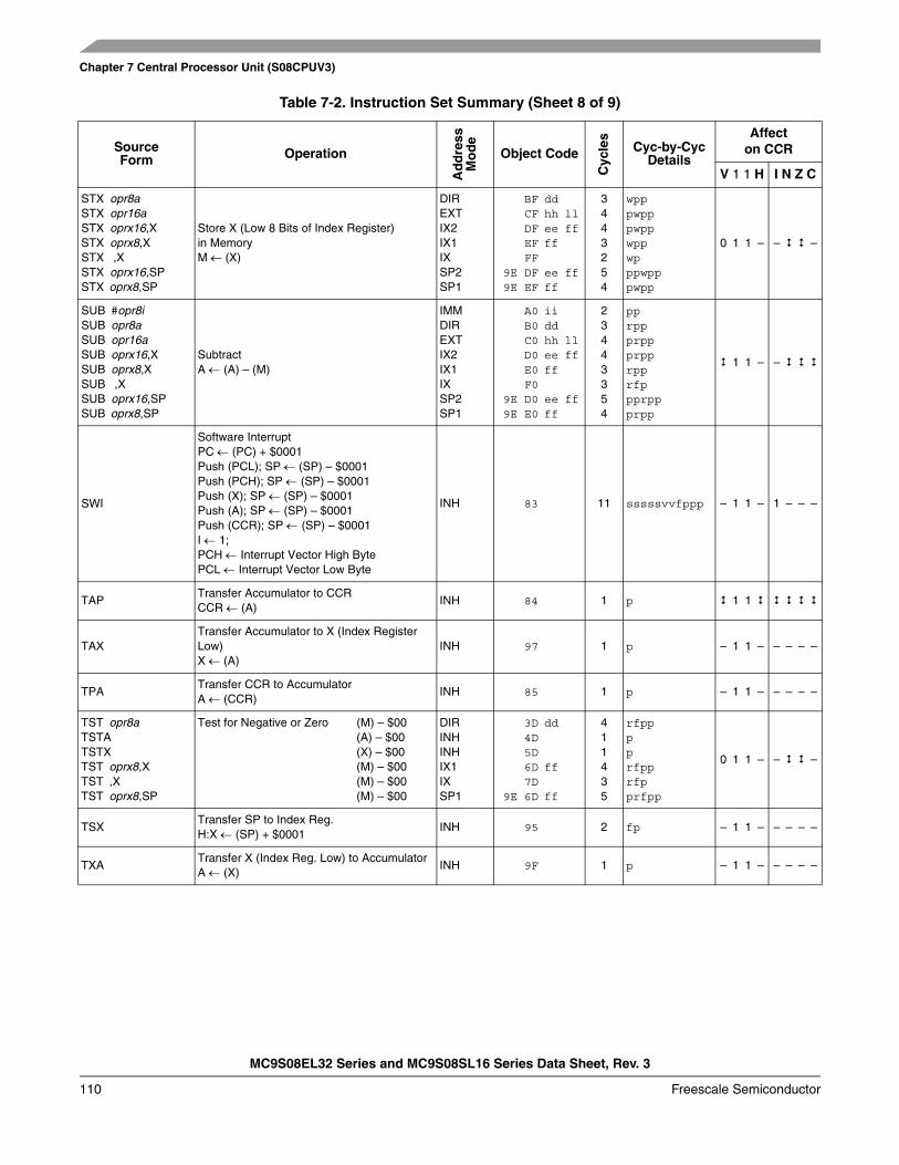
Chapter 7 Central Processor Unit (S08CPUV3)
MC9S08EL32 Series and MC9S08SL16 Series Data Sheet, Rev. 3
110 Freescale Semiconductor
STX opr8aSTX opr16aSTX oprx16,XSTX oprx8,XSTX ,XSTX oprx16,SPSTX oprx8,SP
Store X (Low 8 Bits of Index Register)in MemoryM ← (X)
DIREXTIX2IX1IXSP2SP1
BFCFDFEFFF
9E DF9E EF
ddhh llee ffff
ee ffff
3443254
wpppwpppwppwppwpppwpppwpp
0 1 1 – – –
SUB #opr8iSUB opr8aSUB opr16aSUB oprx16,XSUB oprx8,XSUB ,XSUB oprx16,SPSUB oprx8,SP
Subtract A ← (A) – (M)
IMMDIREXTIX2IX1IXSP2SP1
A0B0C0D0E0F0
9E D09E E0
iiddhh llee ffff
ee ffff
23443354
pprppprppprpprpprfppprppprpp
1 1 – –
SWI
Software InterruptPC ← (PC) + $0001Push (PCL); SP ← (SP) – $0001Push (PCH); SP ← (SP) – $0001Push (X); SP ← (SP) – $0001Push (A); SP ← (SP) – $0001Push (CCR); SP ← (SP) – $0001I ← 1;PCH ← Interrupt Vector High BytePCL ← Interrupt Vector Low Byte
INH 83 11 sssssvvfppp – 1 1 – 1 – – –
TAPTransfer Accumulator to CCRCCR ← (A)
INH 84 1 p 1 1
TAXTransfer Accumulator to X (Index Register Low)X ← (A)
INH 97 1 p – 1 1 – – – – –
TPATransfer CCR to AccumulatorA ← (CCR)
INH 85 1 p – 1 1 – – – – –
TST opr8aTSTATSTXTST oprx8,XTST ,XTST oprx8,SP
Test for Negative or Zero (M) – $00(A) – $00(X) – $00(M) – $00(M) – $00(M) – $00
DIRINHINHIX1IXSP1
3D4D5D6D7D
9E 6D
dd
ff
ff
411435
rfpppprfpprfpprfpp
0 1 1 – – –
TSXTransfer SP to Index Reg.H:X ← (SP) + $0001
INH 95 2 fp – 1 1 – – – – –
TXATransfer X (Index Reg. Low) to AccumulatorA ← (X)
INH 9F 1 p – 1 1 – – – – –
Table 7-2. Instruction Set Summary (Sheet 8 of 9)
SourceForm Operation
Ad
dre
ssM
od
e
Object Code
Cyc
les
Cyc-by-Cyc Details
Affecton CCR
V 1 1 H I N Z C
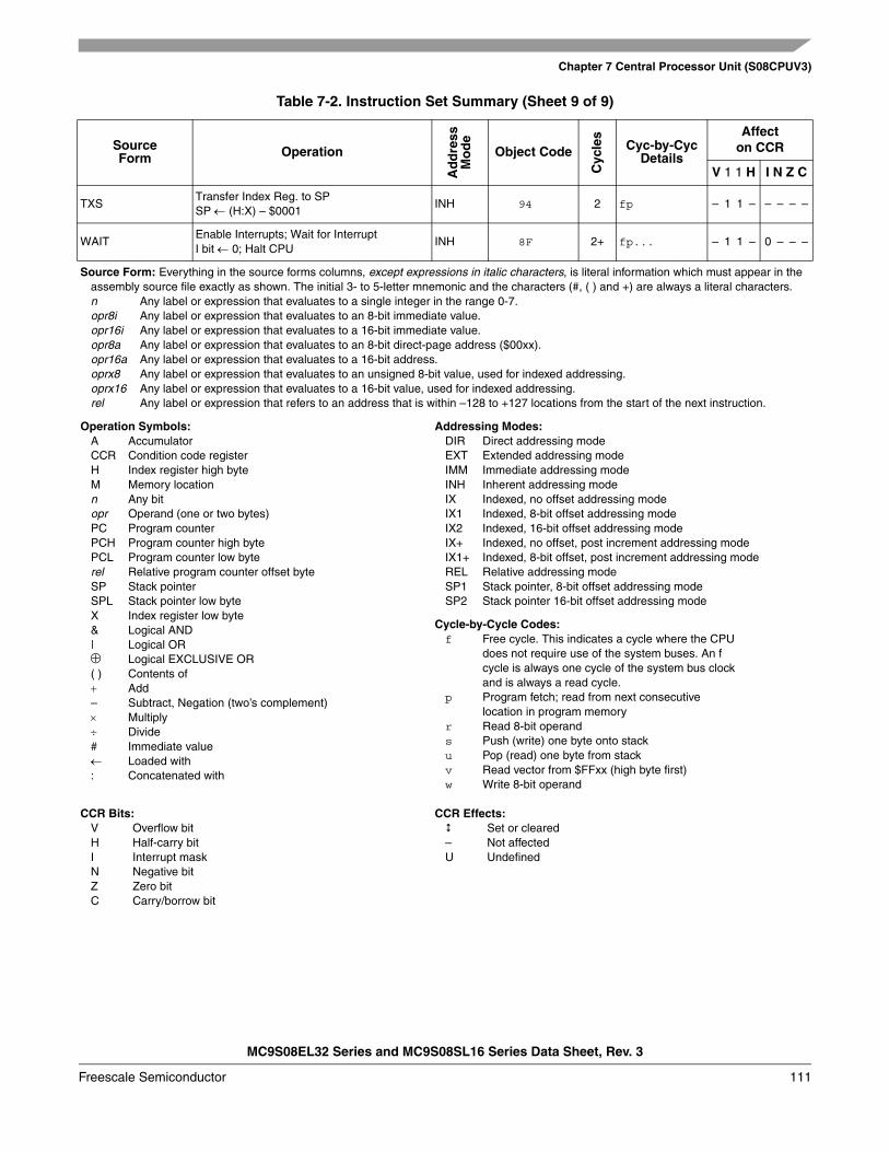
Chapter 7 Central Processor Unit (S08CPUV3)
MC9S08EL32 Series and MC9S08SL16 Series Data Sheet, Rev. 3
Freescale Semiconductor 111
TXSTransfer Index Reg. to SPSP ← (H:X) – $0001
INH 94 2 fp – 1 1 – – – – –
WAITEnable Interrupts; Wait for InterruptI bit ← 0; Halt CPU
INH 8F 2+ fp... – 1 1 – 0 – – –
Source Form: Everything in the source forms columns, except expressions in italic characters, is literal information which must appear in the assembly source file exactly as shown. The initial 3- to 5-letter mnemonic and the characters (#, ( ) and +) are always a literal characters.n Any label or expression that evaluates to a single integer in the range 0-7.opr8i Any label or expression that evaluates to an 8-bit immediate value.opr16i Any label or expression that evaluates to a 16-bit immediate value.opr8a Any label or expression that evaluates to an 8-bit direct-page address ($00xx).opr16a Any label or expression that evaluates to a 16-bit address.oprx8 Any label or expression that evaluates to an unsigned 8-bit value, used for indexed addressing.oprx16 Any label or expression that evaluates to a 16-bit value, used for indexed addressing.rel Any label or expression that refers to an address that is within –128 to +127 locations from the start of the next instruction.
Operation Symbols:A AccumulatorCCR Condition code registerH Index register high byteM Memory locationn Any bitopr Operand (one or two bytes)PC Program counterPCH Program counter high bytePCL Program counter low byterel Relative program counter offset byteSP Stack pointerSPL Stack pointer low byteX Index register low byte& Logical AND| Logical OR⊕ Logical EXCLUSIVE OR( ) Contents of+ Add– Subtract, Negation (two’s complement)× Multiply÷ Divide# Immediate value← Loaded with: Concatenated with
Addressing Modes:DIR Direct addressing modeEXT Extended addressing modeIMM Immediate addressing modeINH Inherent addressing modeIX Indexed, no offset addressing modeIX1 Indexed, 8-bit offset addressing modeIX2 Indexed, 16-bit offset addressing modeIX+ Indexed, no offset, post increment addressing modeIX1+ Indexed, 8-bit offset, post increment addressing modeREL Relative addressing modeSP1 Stack pointer, 8-bit offset addressing modeSP2 Stack pointer 16-bit offset addressing mode
Cycle-by-Cycle Codes:f Free cycle. This indicates a cycle where the CPU
does not require use of the system buses. An fcycle is always one cycle of the system bus clockand is always a read cycle.
p Program fetch; read from next consecutive location in program memory
r Read 8-bit operands Push (write) one byte onto stacku Pop (read) one byte from stackv Read vector from $FFxx (high byte first)w Write 8-bit operand
CCR Bits:V Overflow bitH Half-carry bitI Interrupt maskN Negative bitZ Zero bitC Carry/borrow bit
CCR Effects:Set or cleared
– Not affectedU Undefined
Table 7-2. Instruction Set Summary (Sheet 9 of 9)
SourceForm Operation
Ad
dre
ssM
od
e
Object Code
Cyc
les
Cyc-by-Cyc Details
Affecton CCR
V 1 1 H I N Z C
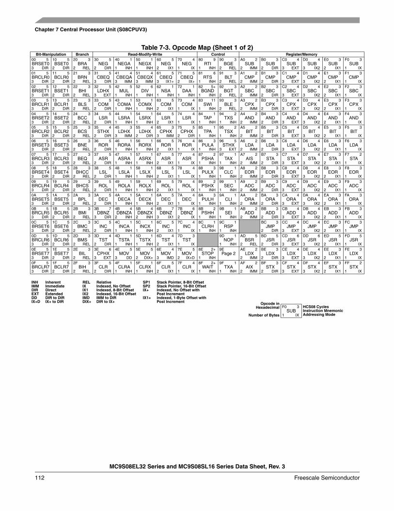
Chapter 7 Central Processor Unit (S08CPUV3)
MC9S08EL32 Series and MC9S08SL16 Series Data Sheet, Rev. 3
112 Freescale Semiconductor
Table 7-3. Opcode Map (Sheet 1 of 2)Bit-Manipulation Branch Read-Modify-Write Control Register/Memory
00 5BRSET03 DIR
10 5BSET0
2 DIR
20 3BRA
2 REL
30 5NEG
2 DIR
40 1NEGA
1 INH
50 1NEGX
1 INH
60 5NEG
2 IX1
70 4NEG
1 IX
80 9RTI
1 INH
90 3BGE
2 REL
A0 2SUB
2 IMM
B0 3SUB
2 DIR
C0 4SUB
3 EXT
D0 4SUB
3 IX2
E0 3SUB
2 IX1
F0 3SUB
1 IX01 5BRCLR03 DIR
11 5BCLR0
2 DIR
21 3BRN
2 REL
31 5CBEQ
3 DIR
41 4CBEQA
3 IMM
51 4CBEQX
3 IMM
61 5CBEQ
3 IX1+
71 5CBEQ
2 IX+
81 6RTS
1 INH
91 3BLT
2 REL
A1 2CMP
2 IMM
B1 3CMP
2 DIR
C1 4CMP
3 EXT
D1 4CMP
3 IX2
E1 3CMP
2 IX1
F1 3CMP
1 IX02 5BRSET13 DIR
12 5BSET1
2 DIR
22 3BHI
2 REL
32 5LDHX
3 EXT
42 5MUL
1 INH
52 6DIV
1 INH
62 1NSA
1 INH
72 1DAA
1 INH
82 5+BGND
1 INH
92 3BGT
2 REL
A2 2SBC
2 IMM
B2 3SBC
2 DIR
C2 4SBC
3 EXT
D2 4SBC
3 IX2
E2 3SBC
2 IX1
F2 3SBC
1 IX03 5BRCLR13 DIR
13 5BCLR1
2 DIR
23 3BLS
2 REL
33 5COM
2 DIR
43 1COMA
1 INH
53 1COMX
1 INH
63 5COM
2 IX1
73 4COM
1 IX
83 11SWI
1 INH
93 3BLE
2 REL
A3 2CPX
2 IMM
B3 3CPX
2 DIR
C3 4CPX
3 EXT
D3 4CPX
3 IX2
E3 3CPX
2 IX1
F3 3CPX
1 IX04 5BRSET23 DIR
14 5BSET2
2 DIR
24 3BCC
2 REL
34 5LSR
2 DIR
44 1LSRA
1 INH
54 1LSRX
1 INH
64 5LSR
2 IX1
74 4LSR
1 IX
84 1TAP
1 INH
94 2TXS
1 INH
A4 2AND
2 IMM
B4 3AND
2 DIR
C4 4AND
3 EXT
D4 4AND
3 IX2
E4 3AND
2 IX1
F4 3AND
1 IX05 5BRCLR23 DIR
15 5BCLR2
2 DIR
25 3BCS
2 REL
35 4STHX
2 DIR
45 3LDHX
3 IMM
55 4LDHX
2 DIR
65 3CPHX
3 IMM
75 5CPHX
2 DIR
85 1TPA
1 INH
95 2TSX
1 INH
A5 2BIT
2 IMM
B5 3BIT
2 DIR
C5 4BIT
3 EXT
D5 4BIT
3 IX2
E5 3BIT
2 IX1
F5 3BIT
1 IX06 5BRSET33 DIR
16 5BSET3
2 DIR
26 3BNE
2 REL
36 5ROR
2 DIR
46 1RORA
1 INH
56 1RORX
1 INH
66 5ROR
2 IX1
76 4ROR
1 IX
86 3PULA
1 INH
96 5STHX
3 EXT
A6 2LDA
2 IMM
B6 3LDA
2 DIR
C6 4LDA
3 EXT
D6 4LDA
3 IX2
E6 3LDA
2 IX1
F6 3LDA
1 IX07 5BRCLR33 DIR
17 5BCLR3
2 DIR
27 3BEQ
2 REL
37 5ASR
2 DIR
47 1ASRA
1 INH
57 1ASRX
1 INH
67 5ASR
2 IX1
77 4ASR
1 IX
87 2PSHA
1 INH
97 1TAX
1 INH
A7 2AIS
2 IMM
B7 3STA
2 DIR
C7 4STA
3 EXT
D7 4STA
3 IX2
E7 3STA
2 IX1
F7 2STA
1 IX08 5BRSET43 DIR
18 5BSET4
2 DIR
28 3BHCC
2 REL
38 5LSL
2 DIR
48 1LSLA
1 INH
58 1LSLX
1 INH
68 5LSL
2 IX1
78 4LSL
1 IX
88 3PULX
1 INH
98 1CLC
1 INH
A8 2EOR
2 IMM
B8 3EOR
2 DIR
C8 4EOR
3 EXT
D8 4EOR
3 IX2
E8 3EOR
2 IX1
F8 3EOR
1 IX09 5BRCLR43 DIR
19 5BCLR4
2 DIR
29 3BHCS
2 REL
39 5ROL
2 DIR
49 1ROLA
1 INH
59 1ROLX
1 INH
69 5ROL
2 IX1
79 4ROL
1 IX
89 2PSHX
1 INH
99 1SEC
1 INH
A9 2ADC
2 IMM
B9 3ADC
2 DIR
C9 4ADC
3 EXT
D9 4ADC
3 IX2
E9 3ADC
2 IX1
F9 3ADC
1 IX0A 5BRSET53 DIR
1A 5BSET5
2 DIR
2A 3BPL
2 REL
3A 5DEC
2 DIR
4A 1DECA
1 INH
5A 1DECX
1 INH
6A 5DEC
2 IX1
7A 4DEC
1 IX
8A 3PULH
1 INH
9A 1CLI
1 INH
AA 2ORA
2 IMM
BA 3ORA
2 DIR
CA 4ORA
3 EXT
DA 4ORA
3 IX2
EA 3ORA
2 IX1
FA 3ORA
1 IX0B 5BRCLR53 DIR
1B 5BCLR5
2 DIR
2B 3BMI
2 REL
3B 7DBNZ
3 DIR
4B 4DBNZA
2 INH
5B 4DBNZX
2 INH
6B 7DBNZ
3 IX1
7B 6DBNZ
2 IX
8B 2PSHH
1 INH
9B 1SEI
1 INH
AB 2ADD
2 IMM
BB 3ADD
2 DIR
CB 4ADD
3 EXT
DB 4ADD
3 IX2
EB 3ADD
2 IX1
FB 3ADD
1 IX0C 5BRSET63 DIR
1C 5BSET6
2 DIR
2C 3BMC
2 REL
3C 5INC
2 DIR
4C 1INCA
1 INH
5C 1INCX
1 INH
6C 5INC
2 IX1
7C 4INC
1 IX
8C 1CLRH
1 INH
9C 1RSP
1 INH
BC 3JMP
2 DIR
CC 4JMP
3 EXT
DC 4JMP
3 IX2
EC 3JMP
2 IX1
FC 3JMP
1 IX0D 5BRCLR63 DIR
1D 5BCLR6
2 DIR
2D 3BMS
2 REL
3D 4TST
2 DIR
4D 1TSTA
1 INH
5D 1TSTX
1 INH
6D 4TST
2 IX1
7D 3TST
1 IX
9D 1NOP
1 INH
AD 5BSR
2 REL
BD 5JSR
2 DIR
CD 6JSR
3 EXT
DD 6JSR
3 IX2
ED 5JSR
2 IX1
FD 5JSR
1 IX0E 5BRSET73 DIR
1E 5BSET7
2 DIR
2E 3BIL
2 REL
3E 6CPHX
3 EXT
4E 5MOV
3 DD
5E 5MOV
2 DIX+
6E 4MOV
3 IMD
7E 5MOV
2 IX+D
8E 2+STOP
1 INH
9EPage 2
AE 2LDX
2 IMM
BE 3LDX
2 DIR
CE 4LDX
3 EXT
DE 4LDX
3 IX2
EE 3LDX
2 IX1
FE 3LDX
1 IX0F 5BRCLR73 DIR
1F 5BCLR7
2 DIR
2F 3BIH
2 REL
3F 5CLR
2 DIR
4F 1CLRA
1 INH
5F 1CLRX
1 INH
6F 5CLR
2 IX1
7F 4CLR
1 IX
8F 2+WAIT
1 INH
9F 1TXA
1 INH
AF 2AIX
2 IMM
BF 3STX
2 DIR
CF 4STX
3 EXT
DF 4STX
3 IX2
EF 3STX
2 IX1
FF 2STX
1 IX
INH Inherent REL Relative SP1 Stack Pointer, 8-Bit OffsetIMM Immediate IX Indexed, No Offset SP2 Stack Pointer, 16-Bit OffsetDIR Direct IX1 Indexed, 8-Bit Offset IX+ Indexed, No Offset with EXT Extended IX2 Indexed, 16-Bit Offset Post IncrementDD DIR to DIR IMD IMM to DIR IX1+ Indexed, 1-Byte Offset with IX+D IX+ to DIR DIX+ DIR to IX+ Post Increment Opcode in
Hexadecimal
Number of Bytes
F0 3SUB
1 IX
HCS08 CyclesInstruction MnemonicAddressing Mode
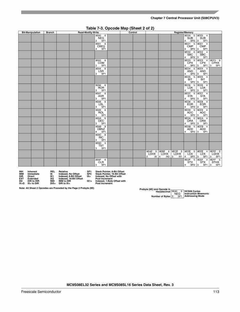
Chapter 7 Central Processor Unit (S08CPUV3)
MC9S08EL32 Series and MC9S08SL16 Series Data Sheet, Rev. 3
Freescale Semiconductor 113
Bit-Manipulation Branch Read-Modify-Write Control Register/Memory9E60 6
NEG3 SP1
9ED0 5SUB
4 SP2
9EE0 4SUB
3 SP19E61 6
CBEQ4 SP1
9ED1 5CMP
4 SP2
9EE1 4CMP
3 SP19ED2 5
SBC4 SP2
9EE2 4SBC
3 SP19E63 6
COM3 SP1
9ED3 5CPX
4 SP2
9EE3 4CPX
3 SP1
9EF3 6CPHX
3 SP19E64 6
LSR3 SP1
9ED4 5AND
4 SP2
9EE4 4AND
3 SP19ED5 5
BIT4 SP2
9EE5 4BIT
3 SP19E66 6
ROR3 SP1
9ED6 5LDA
4 SP2
9EE6 4LDA
3 SP19E67 6
ASR3 SP1
9ED7 5STA
4 SP2
9EE7 4STA
3 SP19E68 6
LSL3 SP1
9ED8 5EOR
4 SP2
9EE8 4EOR
3 SP19E69 6
ROL3 SP1
9ED9 5ADC
4 SP2
9EE9 4ADC
3 SP19E6A 6
DEC3 SP1
9EDA 5ORA
4 SP2
9EEA 4ORA
3 SP19E6B 8
DBNZ4 SP1
9EDB 5ADD
4 SP2
9EEB 4ADD
3 SP19E6C 6
INC3 SP19E6D 5
TST3 SP1
9EAE 5LDHX
2 IX
9EBE 6LDHX
4 IX2
9ECE 5LDHX
3 IX1
9EDE 5LDX
4 SP2
9EEE 4LDX
3 SP1
9EFE 5LDHX
3 SP19E6F 6
CLR3 SP1
9EDF 5STX
4 SP2
9EEF 4STX
3 SP1
9EFF 5STHX
3 SP1
INH Inherent REL Relative SP1 Stack Pointer, 8-Bit OffsetIMM Immediate IX Indexed, No Offset SP2 Stack Pointer, 16-Bit OffsetDIR Direct IX1 Indexed, 8-Bit Offset IX+ Indexed, No Offset with EXT Extended IX2 Indexed, 16-Bit Offset Post IncrementDD DIR to DIR IMD IMM to DIR IX1+ Indexed, 1-Byte Offset with IX+D IX+ to DIR DIX+ DIR to IX+ Post Increment
Note: All Sheet 2 Opcodes are Preceded by the Page 2 Prebyte (9E) Prebyte (9E) and Opcode inHexadecimal
Number of Bytes
9E60 6NEG
3 SP1
HCS08 CyclesInstruction MnemonicAddressing Mode
Table 7-3. Opcode Map (Sheet 2 of 2)

Chapter 7 Central Processor Unit (S08CPUV3)
MC9S08EL32 Series and MC9S08SL16 Series Data Sheet, Rev. 3
114 Freescale Semiconductor
MC9S08EL32 Series and MC9S08SL16 Series Data Sheet, Rev. 3
Freescale Semiconductor 115
Chapter 8 Internal Clock Source (S08ICSV2)
8.1 IntroductionThe internal clock source (ICS) module provides clock source choices for the MCU. The module contains a frequency-locked loop (FLL) as a clock source that is controllable by either an internal or an external reference clock. The module can provide this FLL clock or either of the internal or external reference clocks as a source for the MCU system clock. There are also signals provided to control a low power oscillator (XOSC) module to allow the use of an external crystal/resonator as the external reference clock.
Whichever clock source is chosen, it is passed through a reduced bus divider (BDIV) which allows a lower final output clock frequency to be derived.
The bus frequency is half of the ICSOUT frequency. After reset, the ICS is configured for FEI mode and BDIV resets to 01 to introduce an extra divide-by-two before ICSOUT. Therefore, the bus frequency is fdco/4. At POR, the TRIM and FTRIM are reset to 0x80 and 0, respectively. Therefore, the dco frequency is fdco_ut. For other resets, the trim settings keep the value that was present before the reset.
NOTERefer to Section 1.3, “System Clock Distribution”, for a detailed view of the distribution of clock sources throughout the MCU.
8.1.1 Module Configuration
When the internal reference is enabled in stop mode (IREFSTEN = 1), the voltage regulator must also be enabled in stop mode by setting the LVDE and LVDSE bits in the SPMSC1 register.
Figure 8-1 shows the MC9S08EL32 block diagram with the ICS highlighted.
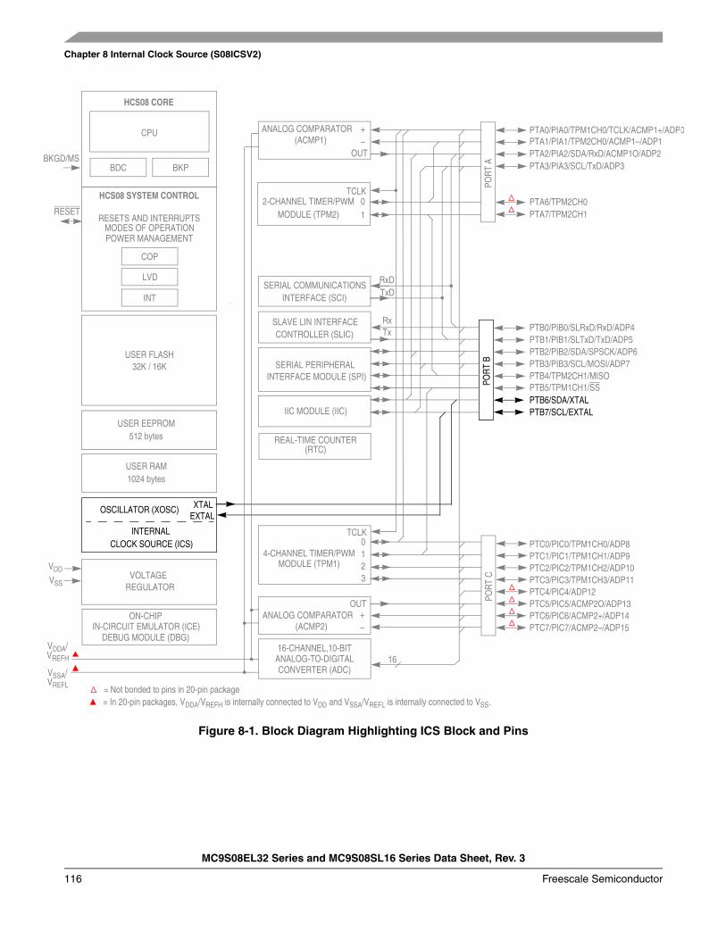
Chapter 8 Internal Clock Source (S08ICSV2)
MC9S08EL32 Series and MC9S08SL16 Series Data Sheet, Rev. 3
116 Freescale Semiconductor
Figure 8-1. Block Diagram Highlighting ICS Block and Pins
VSS
IIC MODULE (IIC)
SERIAL PERIPHERAL INTERFACE MODULE (SPI)
USER FLASH
USER RAM
32K / 16K
HCS08 CORE
CPU
BDC
2-CHANNEL TIMER/PWMMODULE (TPM2)
HCS08 SYSTEM CONTROL
RESETS AND INTERRUPTSMODES OF OPERATIONPOWER MANAGEMENT
VOLTAGE REGULATOR
COP
LVD
OSCILLATOR (XOSC)
INTERNALCLOCK SOURCE (ICS)
RESET
VREFH
1024 bytes
INTERFACE (SCI)SERIAL COMMUNICATIONS
XTALEXTAL
4-CHANNEL TIMER/PWMMODULE (TPM1)
REAL-TIME COUNTER
IN-CIRCUIT EMULATOR (ICE)
BKGD/MS PTA3/PIA3/SCL/TxD/ADP3
PTA6/TPM2CH0
PTA2/PIA2/SDA/RxD/ACMP1O/ADP2PTA1/PIA1/TPM2CH0/ACMP1–/ADP1PTA0/PIA0/TPM1CH0/TCLK/ACMP1+/ADP0
PTA7/TPM2CH1
PTB3/PIB3/SCL/MOSI/ADP7PTB4/TPM2CH1/MISO
PTB2/PIB2/SDA/SPSCK/ADP6PTB1/PIB1/SLTxD/TxD/ADP5PTB0/PIB0/SLRxD/RxD/ADP4
PTB7/SCL/EXTAL
PTC3/PIC3/TPM1CH3/ADP11PTC4/PIC4/ADP12PTC5/PIC5/ACMP2O/ADP13
PTC2/PIC2/TPM1CH2/ADP10PTC1/PIC1/TPM1CH1/ADP9
POR
T C
PTC6/PIC6/ACMP2+/ADP14
VDD
BKP
INT
ANALOG COMPARATOR(ACMP2)
USER EEPROM512 bytes
CONTROLLER (SLIC)SLAVE LIN INTERFACE
ANALOG-TO-DIGITALCONVERTER (ADC)
16-CHANNEL,10-BIT16
= In 20-pin packages, VDDA/VREFH is internally connected to VDD and VSSA/VREFL is internally connected to VSS.
VDDA/
VREFL
VSSA/
DEBUG MODULE (DBG)
ON-CHIP
(RTC)
PTC0/PIC0/TPM1CH0/ADP8
PTC7/PIC7/ACMP2–/ADP15
PTB6/SDA/XTAL
POR
T B
POR
T A
PTB5/TPM1CH1/SS
ANALOG COMPARATOR(ACMP1)
= Not bonded to pins in 20-pin package
TCLK
TCLK
+–
OUT
+–
OUT
0123
10
RxDTxD
TxRx
Internal Clock Source (S08ICSV2)
MC9S08EL32 Series and MC9S08SL16 Series Data Sheet, Rev. 3
Freescale Semiconductor 117
8.1.2 Features
Key features of the ICS module follow. For device specific information, refer to the ICS Characteristics in the Electricals section of the documentation.
• Frequency-locked loop (FLL) is trimmable for accuracy— 0.2% resolution using internal 32kHz reference— 2% deviation over voltage and temperature using internal 32kHz reference
• Internal or external reference clocks up to 5MHz can be used to control the FLL— 3 bit select for reference divider is provided
• Internal reference clock has 9 trim bits available• Internal or external reference clocks can be selected as the clock source for the MCU• Whichever clock is selected as the source can be divided down
— 2 bit select for clock divider is provided– Allowable dividers are: 1, 2, 4, 8– BDC clock is provided as a constant divide by 2 of the DCO output
• Control signals for a low power oscillator as the external reference clock are provided— HGO, RANGE, EREFS, ERCLKEN, EREFSTEN
• FLL Engaged Internal mode is automatically selected out of reset
8.1.3 Block Diagram
Figure 8-2 is the ICS block diagram.
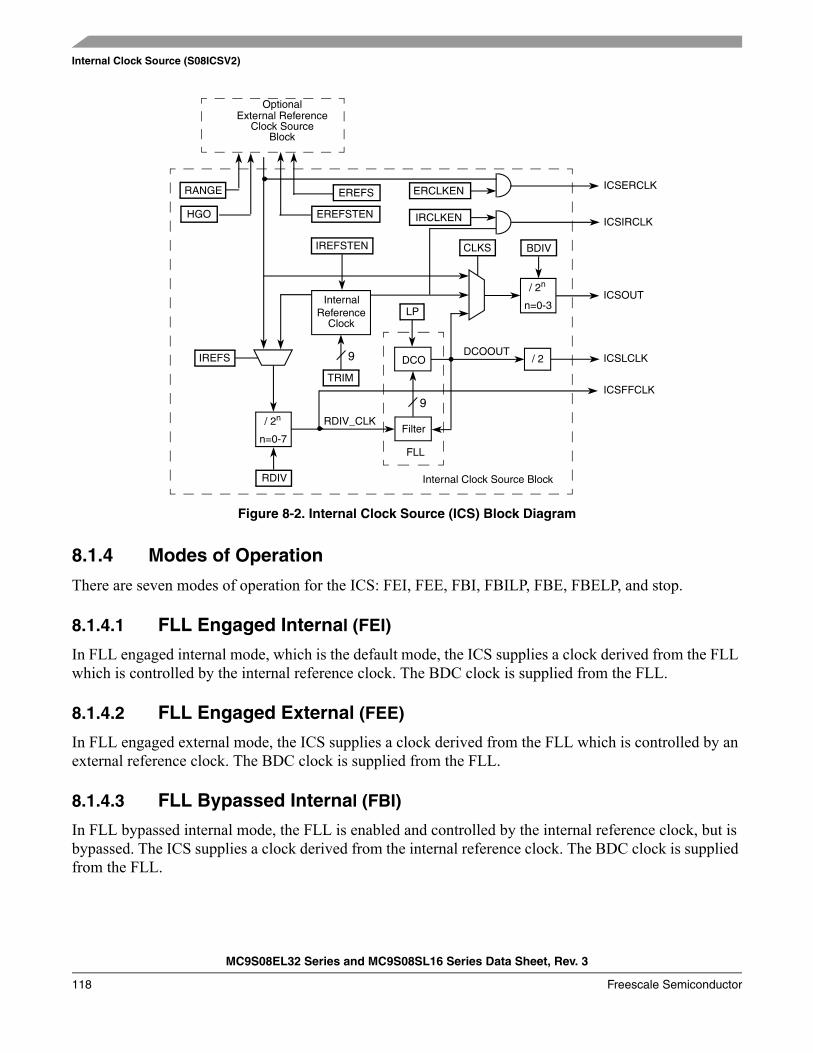
Internal Clock Source (S08ICSV2)
MC9S08EL32 Series and MC9S08SL16 Series Data Sheet, Rev. 3
118 Freescale Semiconductor
Figure 8-2. Internal Clock Source (ICS) Block Diagram
8.1.4 Modes of Operation
There are seven modes of operation for the ICS: FEI, FEE, FBI, FBILP, FBE, FBELP, and stop.
8.1.4.1 FLL Engaged Internal (FEI)
In FLL engaged internal mode, which is the default mode, the ICS supplies a clock derived from the FLL which is controlled by the internal reference clock. The BDC clock is supplied from the FLL.
8.1.4.2 FLL Engaged External (FEE)
In FLL engaged external mode, the ICS supplies a clock derived from the FLL which is controlled by an external reference clock. The BDC clock is supplied from the FLL.
8.1.4.3 FLL Bypassed Internal (FBI)
In FLL bypassed internal mode, the FLL is enabled and controlled by the internal reference clock, but is bypassed. The ICS supplies a clock derived from the internal reference clock. The BDC clock is supplied from the FLL.
DCO
Filter
RDIV
TRIM
/ 2
9
External Reference
IREFS
Clock SourceBlock
CLKS
n=0-7
/ 2n
n=0-3
/ 2n
InternalReference
Clock
BDIV
9 ICSLCLK
ICSOUT
ICSIRCLK
EREFSRANGE
EREFSTENHGO
Optional
IREFSTEN
ICSERCLK
Internal Clock Source Block
LP
ICSFFCLK
ERCLKEN
IRCLKEN
DCOOUT
FLL
RDIV_CLK
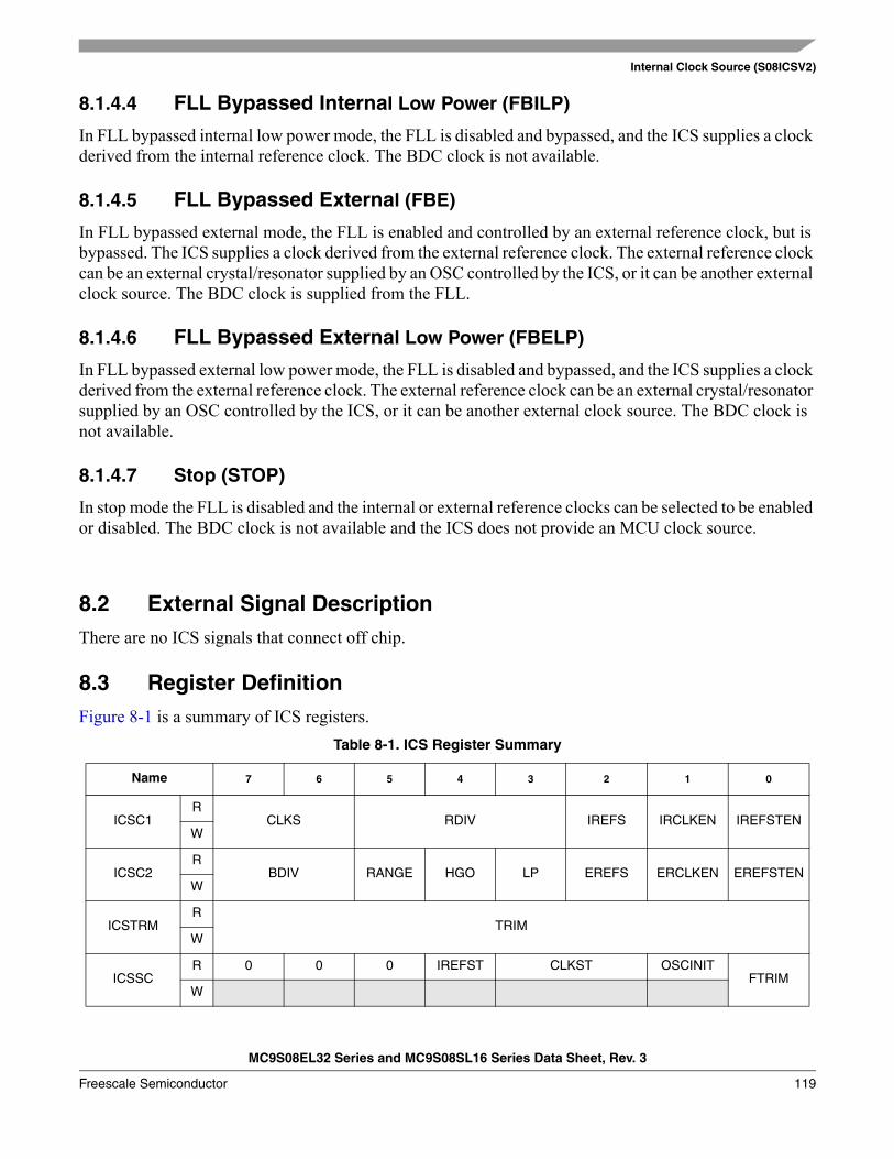
Internal Clock Source (S08ICSV2)
MC9S08EL32 Series and MC9S08SL16 Series Data Sheet, Rev. 3
Freescale Semiconductor 119
8.1.4.4 FLL Bypassed Internal Low Power (FBILP)
In FLL bypassed internal low power mode, the FLL is disabled and bypassed, and the ICS supplies a clock derived from the internal reference clock. The BDC clock is not available.
8.1.4.5 FLL Bypassed External (FBE)
In FLL bypassed external mode, the FLL is enabled and controlled by an external reference clock, but is bypassed. The ICS supplies a clock derived from the external reference clock. The external reference clock can be an external crystal/resonator supplied by an OSC controlled by the ICS, or it can be another external clock source. The BDC clock is supplied from the FLL.
8.1.4.6 FLL Bypassed External Low Power (FBELP)
In FLL bypassed external low power mode, the FLL is disabled and bypassed, and the ICS supplies a clock derived from the external reference clock. The external reference clock can be an external crystal/resonator supplied by an OSC controlled by the ICS, or it can be another external clock source. The BDC clock is not available.
8.1.4.7 Stop (STOP)
In stop mode the FLL is disabled and the internal or external reference clocks can be selected to be enabled or disabled. The BDC clock is not available and the ICS does not provide an MCU clock source.
8.2 External Signal DescriptionThere are no ICS signals that connect off chip.
8.3 Register DefinitionFigure 8-1 is a summary of ICS registers.
Table 8-1. ICS Register Summary
Name 7 6 5 4 3 2 1 0
ICSC1 R
CLKS RDIV IREFS IRCLKEN IREFSTENW
ICSC2R
BDIV RANGE HGO LP EREFS ERCLKEN EREFSTENW
ICSTRMR
TRIMW
ICSSCR 0 0 0 IREFST CLKST OSCINIT
FTRIMW
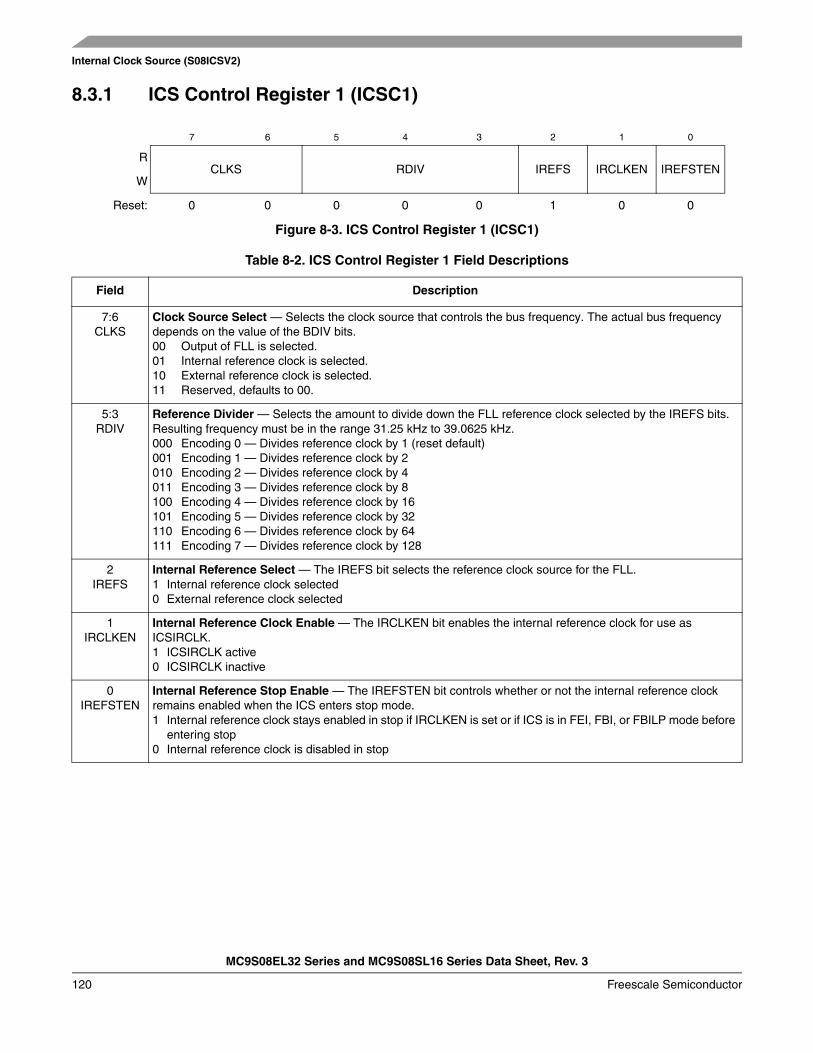
Internal Clock Source (S08ICSV2)
MC9S08EL32 Series and MC9S08SL16 Series Data Sheet, Rev. 3
120 Freescale Semiconductor
8.3.1 ICS Control Register 1 (ICSC1)
7 6 5 4 3 2 1 0
RCLKS RDIV IREFS IRCLKEN IREFSTEN
W
Reset: 0 0 0 0 0 1 0 0
Figure 8-3. ICS Control Register 1 (ICSC1)
Table 8-2. ICS Control Register 1 Field Descriptions
Field Description
7:6CLKS
Clock Source Select — Selects the clock source that controls the bus frequency. The actual bus frequency depends on the value of the BDIV bits.00 Output of FLL is selected.01 Internal reference clock is selected.10 External reference clock is selected.11 Reserved, defaults to 00.
5:3RDIV
Reference Divider — Selects the amount to divide down the FLL reference clock selected by the IREFS bits. Resulting frequency must be in the range 31.25 kHz to 39.0625 kHz.000 Encoding 0 — Divides reference clock by 1 (reset default)001 Encoding 1 — Divides reference clock by 2010 Encoding 2 — Divides reference clock by 4011 Encoding 3 — Divides reference clock by 8100 Encoding 4 — Divides reference clock by 16101 Encoding 5 — Divides reference clock by 32110 Encoding 6 — Divides reference clock by 64111 Encoding 7 — Divides reference clock by 128
2IREFS
Internal Reference Select — The IREFS bit selects the reference clock source for the FLL.1 Internal reference clock selected0 External reference clock selected
1IRCLKEN
Internal Reference Clock Enable — The IRCLKEN bit enables the internal reference clock for use as ICSIRCLK.1 ICSIRCLK active0 ICSIRCLK inactive
0IREFSTEN
Internal Reference Stop Enable — The IREFSTEN bit controls whether or not the internal reference clock remains enabled when the ICS enters stop mode.1 Internal reference clock stays enabled in stop if IRCLKEN is set or if ICS is in FEI, FBI, or FBILP mode before
entering stop0 Internal reference clock is disabled in stop
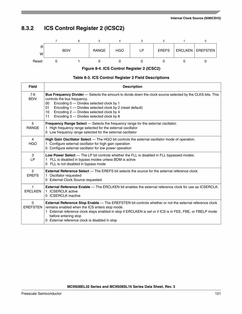
Internal Clock Source (S08ICSV2)
MC9S08EL32 Series and MC9S08SL16 Series Data Sheet, Rev. 3
Freescale Semiconductor 121
8.3.2 ICS Control Register 2 (ICSC2)
7 6 5 4 3 2 1 0
RBDIV RANGE HGO LP EREFS ERCLKEN EREFSTEN
W
Reset: 0 1 0 0 0 0 0 0
Figure 8-4. ICS Control Register 2 (ICSC2)
Table 8-3. ICS Control Register 2 Field Descriptions
Field Description
7:6BDIV
Bus Frequency Divider — Selects the amount to divide down the clock source selected by the CLKS bits. This controls the bus frequency.00 Encoding 0 — Divides selected clock by 101 Encoding 1 — Divides selected clock by 2 (reset default)10 Encoding 2 — Divides selected clock by 411 Encoding 3 — Divides selected clock by 8
5RANGE
Frequency Range Select — Selects the frequency range for the external oscillator.1 High frequency range selected for the external oscillator0 Low frequency range selected for the external oscillator
4HGO
High Gain Oscillator Select — The HGO bit controls the external oscillator mode of operation.1 Configure external oscillator for high gain operation0 Configure external oscillator for low power operation
3LP
Low Power Select — The LP bit controls whether the FLL is disabled in FLL bypassed modes.1 FLL is disabled in bypass modes unless BDM is active0 FLL is not disabled in bypass mode
2EREFS
External Reference Select — The EREFS bit selects the source for the external reference clock.1 Oscillator requested0 External Clock Source requested
1ERCLKEN
External Reference Enable — The ERCLKEN bit enables the external reference clock for use as ICSERCLK.1 ICSERCLK active0 ICSERCLK inactive
0 EREFSTEN
External Reference Stop Enable — The EREFSTEN bit controls whether or not the external reference clock remains enabled when the ICS enters stop mode.1 External reference clock stays enabled in stop if ERCLKEN is set or if ICS is in FEE, FBE, or FBELP mode
before entering stop0 External reference clock is disabled in stop
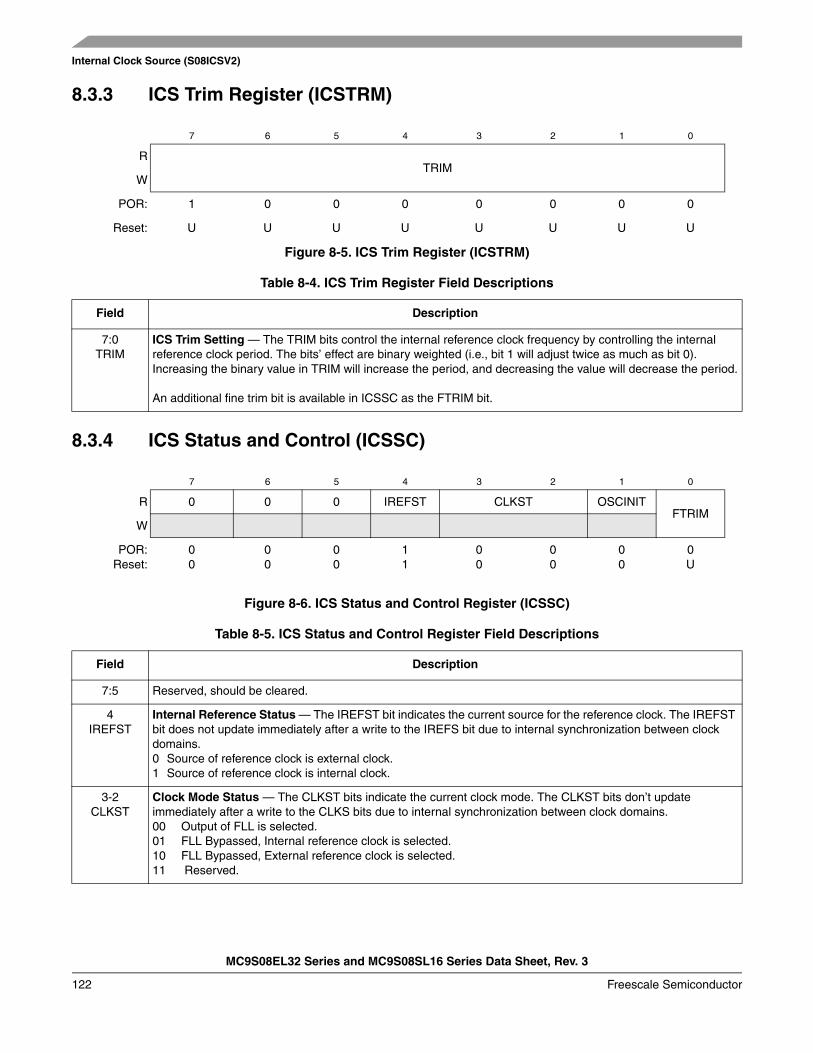
Internal Clock Source (S08ICSV2)
MC9S08EL32 Series and MC9S08SL16 Series Data Sheet, Rev. 3
122 Freescale Semiconductor
8.3.3 ICS Trim Register (ICSTRM)
8.3.4 ICS Status and Control (ICSSC)
7 6 5 4 3 2 1 0
RTRIM
W
POR: 1 0 0 0 0 0 0 0
Reset: U U U U U U U U
Figure 8-5. ICS Trim Register (ICSTRM)
Table 8-4. ICS Trim Register Field Descriptions
Field Description
7:0TRIM
ICS Trim Setting — The TRIM bits control the internal reference clock frequency by controlling the internal reference clock period. The bits’ effect are binary weighted (i.e., bit 1 will adjust twice as much as bit 0). Increasing the binary value in TRIM will increase the period, and decreasing the value will decrease the period.
An additional fine trim bit is available in ICSSC as the FTRIM bit.
7 6 5 4 3 2 1 0
R 0 0 0 IREFST CLKST OSCINITFTRIM
W
POR:Reset:
00
00
00
11
00
00
00
0U
Figure 8-6. ICS Status and Control Register (ICSSC)
Table 8-5. ICS Status and Control Register Field Descriptions
Field Description
7:5 Reserved, should be cleared.
4IREFST
Internal Reference Status — The IREFST bit indicates the current source for the reference clock. The IREFST bit does not update immediately after a write to the IREFS bit due to internal synchronization between clock domains.0 Source of reference clock is external clock.1 Source of reference clock is internal clock.
3-2CLKST
Clock Mode Status — The CLKST bits indicate the current clock mode. The CLKST bits don’t update immediately after a write to the CLKS bits due to internal synchronization between clock domains.00 Output of FLL is selected.01 FLL Bypassed, Internal reference clock is selected.10 FLL Bypassed, External reference clock is selected.11 Reserved.
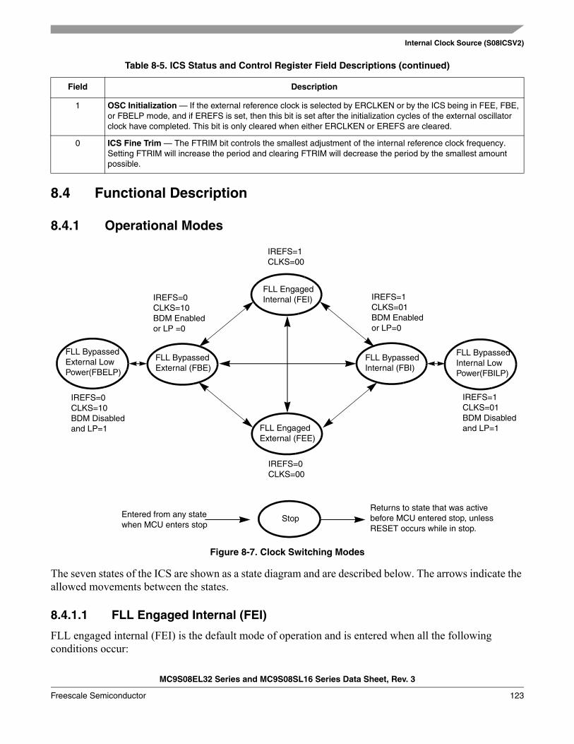
Internal Clock Source (S08ICSV2)
MC9S08EL32 Series and MC9S08SL16 Series Data Sheet, Rev. 3
Freescale Semiconductor 123
8.4 Functional Description
8.4.1 Operational Modes
Figure 8-7. Clock Switching Modes
The seven states of the ICS are shown as a state diagram and are described below. The arrows indicate the allowed movements between the states.
8.4.1.1 FLL Engaged Internal (FEI)
FLL engaged internal (FEI) is the default mode of operation and is entered when all the following conditions occur:
1 OSC Initialization — If the external reference clock is selected by ERCLKEN or by the ICS being in FEE, FBE, or FBELP mode, and if EREFS is set, then this bit is set after the initialization cycles of the external oscillator clock have completed. This bit is only cleared when either ERCLKEN or EREFS are cleared.
0 ICS Fine Trim — The FTRIM bit controls the smallest adjustment of the internal reference clock frequency. Setting FTRIM will increase the period and clearing FTRIM will decrease the period by the smallest amount possible.
Table 8-5. ICS Status and Control Register Field Descriptions (continued)
Field Description
FLL Bypassed Internal Low Power(FBILP)
IREFS=1CLKS=00
Entered from any state when MCU enters stop
FLL Engaged Internal (FEI)
FLL Bypassed Internal (FBI)
FLL Bypassed External (FBE)
FLL Engaged External (FEE)
FLL Bypassed External Low Power(FBELP)
IREFS=0CLKS=00
IREFS=0CLKS=10BDM Enabledor LP =0
Returns to state that was active before MCU entered stop, unless RESET occurs while in stop.
IREFS=0CLKS=10BDM Disabledand LP=1
IREFS=1CLKS=01BDM Enabledor LP=0
IREFS=1CLKS=01BDM Disabledand LP=1
Stop
Internal Clock Source (S08ICSV2)
MC9S08EL32 Series and MC9S08SL16 Series Data Sheet, Rev. 3
124 Freescale Semiconductor
• CLKS bits are written to 00• IREFS bit is written to 1• RDIV bits are written to divide trimmed reference clock to be within the range of 31.25 kHz to
39.0625 kHz.
In FLL engaged internal mode, the ICSOUT clock is derived from the FLL clock, which is controlled by the internal reference clock. The FLL loop will lock the frequency to 1024 times the reference frequency, as selected by the RDIV bits. The ICSLCLK is available for BDC communications, and the internal reference clock is enabled.
8.4.1.2 FLL Engaged External (FEE)
The FLL engaged external (FEE) mode is entered when all the following conditions occur:
• CLKS bits are written to 00• IREFS bit is written to 0• RDIV bits are written to divide reference clock to be within the range of 31.25 kHz to 39.0625 kHz
In FLL engaged external mode, the ICSOUT clock is derived from the FLL clock which is controlled by the external reference clock.The FLL loop will lock the frequency to 1024 times the reference frequency, as selected by the RDIV bits. The ICSLCLK is available for BDC communications, and the external reference clock is enabled.
8.4.1.3 FLL Bypassed Internal (FBI)
The FLL bypassed internal (FBI) mode is entered when all the following conditions occur:• CLKS bits are written to 01• IREFS bit is written to 1.• BDM mode is active or LP bit is written to 0
In FLL bypassed internal mode, the ICSOUT clock is derived from the internal reference clock. The FLL clock is controlled by the internal reference clock, and the FLL loop will lock the FLL frequency to 1024 times the reference frequency, as selected by the RDIV bits. The ICSLCLK will be available for BDC communications, and the internal reference clock is enabled.
8.4.1.4 FLL Bypassed Internal Low Power (FBILP)
The FLL bypassed internal low power (FBILP) mode is entered when all the following conditions occur:• CLKS bits are written to 01• IREFS bit is written to 1.• BDM mode is not active and LP bit is written to 1
In FLL bypassed internal low power mode, the ICSOUT clock is derived from the internal reference clock and the FLL is disabled. The ICSLCLK will be not be available for BDC communications, and the internal reference clock is enabled.
Internal Clock Source (S08ICSV2)
MC9S08EL32 Series and MC9S08SL16 Series Data Sheet, Rev. 3
Freescale Semiconductor 125
8.4.1.5 FLL Bypassed External (FBE)
The FLL bypassed external (FBE) mode is entered when all the following conditions occur:• CLKS bits are written to 10.• IREFS bit is written to 0.• BDM mode is active or LP bit is written to 0.
In FLL bypassed external mode, the ICSOUT clock is derived from the external reference clock. The FLL clock is controlled by the external reference clock, and the FLL loop will lock the FLL frequency to 1024 times the reference frequency, as selected by the RDIV bits, so that the ICSLCLK will be available for BDC communications, and the external reference clock is enabled.
8.4.1.6 FLL Bypassed External Low Power (FBELP)
The FLL bypassed external low power (FBELP) mode is entered when all the following conditions occur:• CLKS bits are written to 10.• IREFS bit is written to 0.• BDM mode is not active and LP bit is written to 1.
In FLL bypassed external low power mode, the ICSOUT clock is derived from the external reference clock and the FLL is disabled. The ICSLCLK will be not be available for BDC communications. The external reference clock is enabled.
8.4.1.7 Stop
Stop mode is entered whenever the MCU enters a STOP state. In this mode, all ICS clock signals are static except in the following cases:
ICSIRCLK will be active in stop mode when all the following conditions occur:• IRCLKEN bit is written to 1• IREFSTEN bit is written to 1
ICSERCLK will be active in stop mode when all the following conditions occur:• ERCLKEN bit is written to 1• EREFSTEN bit is written to 1
8.4.2 Mode Switching
When switching between FLL engaged internal (FEI) and FLL engaged external (FEE) modes the IREFS bit can be changed at anytime, but the RDIV bits must be changed simultaneously so that the resulting frequency stays in the range of 31.25 kHz to 39.0625 kHz. After a change in the IREFS value the FLL will begin locking again after a few full cycles of the resulting divided reference frequency. The completion of the switch is shown by the IREFST bit.
Internal Clock Source (S08ICSV2)
MC9S08EL32 Series and MC9S08SL16 Series Data Sheet, Rev. 3
126 Freescale Semiconductor
The CLKS bits can also be changed at anytime, but the RDIV bits must be changed simultaneously so that the resulting frequency stays in the range of 31.25 kHz to 39.0625 kHz. The actual switch to the newly selected clock will not occur until after a few full cycles of the new clock. If the newly selected clock is not available, the previous clock will remain selected.
8.4.3 Bus Frequency Divider
The BDIV bits can be changed at anytime and the actual switch to the new frequency will occur immediately.
8.4.4 Low Power Bit Usage
The low power bit (LP) is provided to allow the FLL to be disabled and thus conserve power when it is not being used. However, in some applications it may be desirable to enable the FLL and allow it to lock for maximum accuracy before switching to an FLL engaged mode. Do this by writing the LP bit to 0.
8.4.5 Internal Reference Clock
When IRCLKEN is set the internal reference clock signal will be presented as ICSIRCLK, which can be used as an additional clock source. The ICSIRCLK frequency can be re-targeted by trimming the period of the internal reference clock. This can be done by writing a new value to the TRIM bits in the ICSTRM register. Writing a larger value will slow down the ICSIRCLK frequency, and writing a smaller value to the ICSTRM register will speed up the ICSIRCLK frequency. The TRIM bits will effect the ICSOUT frequency if the ICS is in FLL engaged internal (FEI), FLL bypassed internal (FBI), or FLL bypassed internal low power (FBILP) mode. The TRIM and FTRIM value will not be affected by a reset.
Until ICSIRCLK is trimmed, programming low reference divider (RDIV) factors may result in ICSOUT frequencies that exceed the maximum chip-level frequency and violate the chip-level clock timing specifications (see the Device Overview chapter).
If IREFSTEN is set and the IRCLKEN bit is written to 1, the internal reference clock will keep running during stop mode in order to provide a fast recovery upon exiting stop.
All MCU devices are factory programmed with a trim value in a reserved memory location. This value can be copied to the ICSTRM register during reset initialization. The factory trim value does not include the FTRIM bit. For finer precision, the user can trim the internal oscillator in the application and set the FTRIM bit accordingly.
8.4.6 Optional External Reference Clock
The ICS module can support an external reference clock with frequencies between 31.25 kHz to 5 MHz in all modes. When the ERCLKEN is set, the external reference clock signal will be presented as ICSERCLK, which can be used as an additional clock source. When IREFS = 1, the external reference clock will not be used by the FLL and will only be used as ICSERCLK. In these modes, the frequency can be equal to the maximum frequency the chip-level timing specifications will support (see the Device Overview chapter).
Internal Clock Source (S08ICSV2)
MC9S08EL32 Series and MC9S08SL16 Series Data Sheet, Rev. 3
Freescale Semiconductor 127
If EREFSTEN is set and the ERCLKEN bit is written to 1, the external reference clock will keep running during stop mode in order to provide a fast recovery upon exiting stop.
8.4.7 Fixed Frequency Clock
The ICS presents the divided FLL reference clock as ICSFFCLK for use as an additional clock source for peripheral modules. The ICS provides an output signal (ICSFFE) which indicates when the ICS is providing ICSOUT frequencies four times or greater than the divided FLL reference clock (ICSFFCLK). In FLL Engaged mode (FEI and FEE) this is always true and ICSFFE is always high. In ICS Bypass modes, ICSFFE will get asserted for the following combinations of BDIV and RDIV values:
• BDIV=00 (divide by 1), RDIV ≥ 010• BDIV=01 (divide by 2), RDIV ≥ 011• BDIV=10 (divide by 4), RDIV ≥ 100• BDIV=11 (divide by 8), RDIV ≥ 101

Internal Clock Source (S08ICSV2)
MC9S08EL32 Series and MC9S08SL16 Series Data Sheet, Rev. 3
128 Freescale Semiconductor
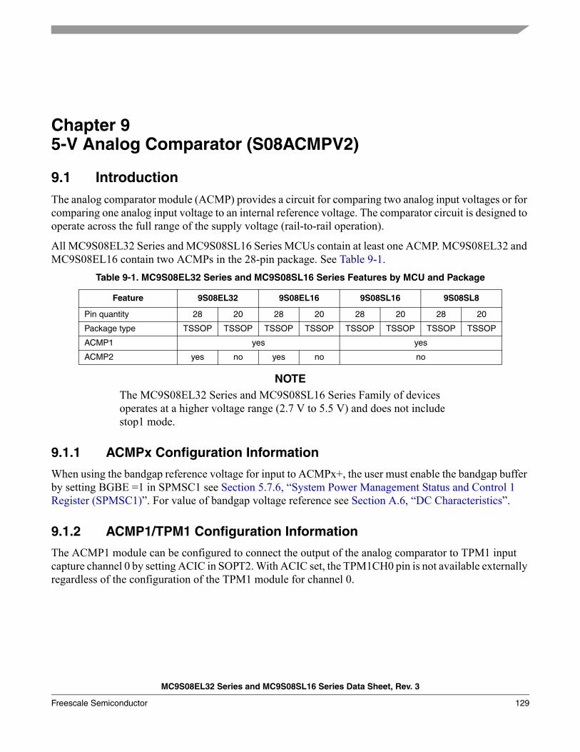
MC9S08EL32 Series and MC9S08SL16 Series Data Sheet, Rev. 3
Freescale Semiconductor 129
Chapter 9 5-V Analog Comparator (S08ACMPV2)
9.1 IntroductionThe analog comparator module (ACMP) provides a circuit for comparing two analog input voltages or for comparing one analog input voltage to an internal reference voltage. The comparator circuit is designed to operate across the full range of the supply voltage (rail-to-rail operation).
All MC9S08EL32 Series and MC9S08SL16 Series MCUs contain at least one ACMP. MC9S08EL32 and MC9S08EL16 contain two ACMPs in the 28-pin package. See Table 9-1.
t
NOTEThe MC9S08EL32 Series and MC9S08SL16 Series Family of devices operates at a higher voltage range (2.7 V to 5.5 V) and does not include stop1 mode.
9.1.1 ACMPx Configuration Information
When using the bandgap reference voltage for input to ACMPx+, the user must enable the bandgap buffer by setting BGBE =1 in SPMSC1 see Section 5.7.6, “System Power Management Status and Control 1 Register (SPMSC1)”. For value of bandgap voltage reference see Section A.6, “DC Characteristics”.
9.1.2 ACMP1/TPM1 Configuration Information
The ACMP1 module can be configured to connect the output of the analog comparator to TPM1 input capture channel 0 by setting ACIC in SOPT2. With ACIC set, the TPM1CH0 pin is not available externally regardless of the configuration of the TPM1 module for channel 0.
Table 9-1. MC9S08EL32 Series and MC9S08SL16 Series Features by MCU and Package
Feature 9S08EL32 9S08EL16 9S08SL16 9S08SL8
Pin quantity 28 20 28 20 28 20 28 20
Package type TSSOP TSSOP TSSOP TSSOP TSSOP TSSOP TSSOP TSSOP
ACMP1 yes yes
ACMP2 yes no yes no no
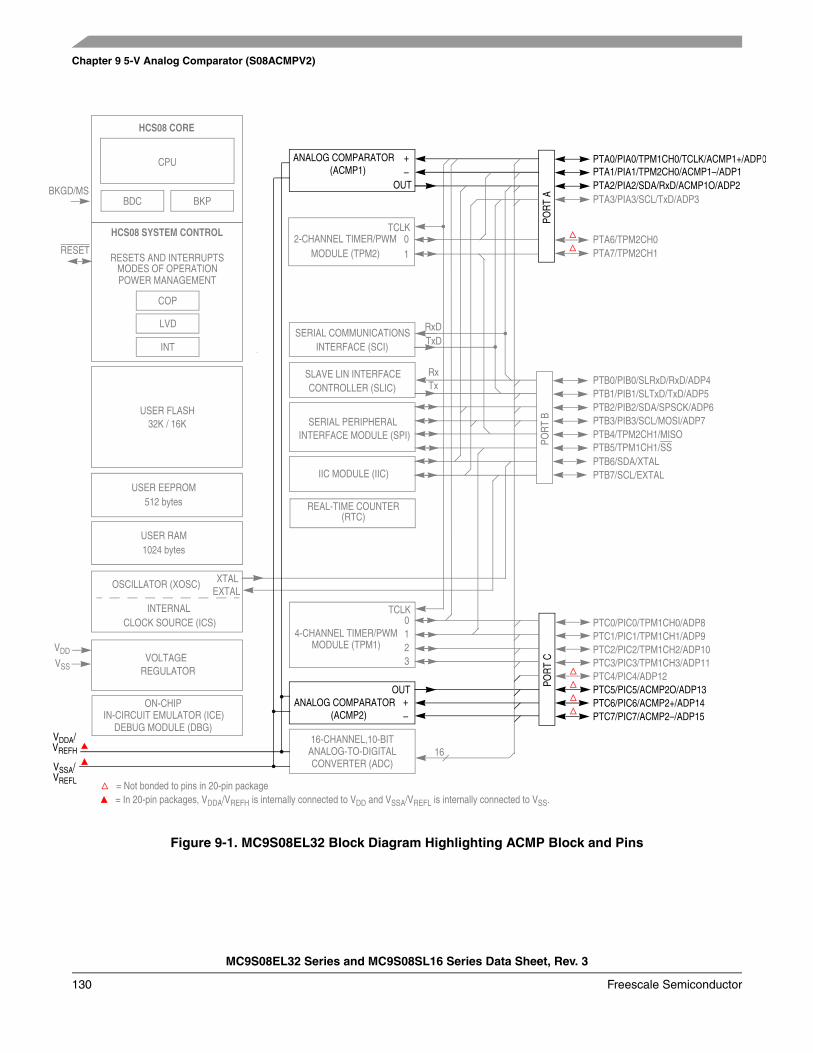
Chapter 9 5-V Analog Comparator (S08ACMPV2)
MC9S08EL32 Series and MC9S08SL16 Series Data Sheet, Rev. 3
130 Freescale Semiconductor
Figure 9-1. MC9S08EL32 Block Diagram Highlighting ACMP Block and Pins
VSS
IIC MODULE (IIC)
SERIAL PERIPHERAL INTERFACE MODULE (SPI)
USER FLASH
USER RAM
32K / 16K
HCS08 CORE
CPU
BDC
2-CHANNEL TIMER/PWMMODULE (TPM2)
HCS08 SYSTEM CONTROL
RESETS AND INTERRUPTSMODES OF OPERATIONPOWER MANAGEMENT
VOLTAGE REGULATOR
COP
LVD
OSCILLATOR (XOSC)
INTERNALCLOCK SOURCE (ICS)
RESET
VREFH
1024 bytes
INTERFACE (SCI)SERIAL COMMUNICATIONS
XTALEXTAL
4-CHANNEL TIMER/PWMMODULE (TPM1)
REAL-TIME COUNTER
IN-CIRCUIT EMULATOR (ICE)
BKGD/MS PTA3/PIA3/SCL/TxD/ADP3
PTA6/TPM2CH0
PTA2/PIA2/SDA/RxD/ACMP1O/ADP2PTA1/PIA1/TPM2CH0/ACMP1–/ADP1PTA0/PIA0/TPM1CH0/TCLK/ACMP1+/ADP0
PTA7/TPM2CH1
PTB3/PIB3/SCL/MOSI/ADP7PTB4/TPM2CH1/MISO
PTB2/PIB2/SDA/SPSCK/ADP6PTB1/PIB1/SLTxD/TxD/ADP5PTB0/PIB0/SLRxD/RxD/ADP4
PTB7/SCL/EXTAL
PTC3/PIC3/TPM1CH3/ADP11PTC4/PIC4/ADP12PTC5/PIC5/ACMP2O/ADP13
PTC2/PIC2/TPM1CH2/ADP10PTC1/PIC1/TPM1CH1/ADP9
POR
T C
PTC6/PIC6/ACMP2+/ADP14
VDD
BKP
INT
ANALOG COMPARATOR(ACMP2)
USER EEPROM512 bytes
CONTROLLER (SLIC)SLAVE LIN INTERFACE
ANALOG-TO-DIGITALCONVERTER (ADC)
16-CHANNEL,10-BIT16
= In 20-pin packages, VDDA/VREFH is internally connected to VDD and VSSA/VREFL is internally connected to VSS.
VDDA/
VREFL
VSSA/
DEBUG MODULE (DBG)
ON-CHIP
(RTC)
PTC0/PIC0/TPM1CH0/ADP8
PTC7/PIC7/ACMP2–/ADP15
PTB6/SDA/XTAL
POR
T B
POR
T A
PTB5/TPM1CH1/SS
ANALOG COMPARATOR(ACMP1)
= Not bonded to pins in 20-pin package
TCLK
TCLK
+–
OUT
+–
OUT
0123
10
RxDTxD
TxRx
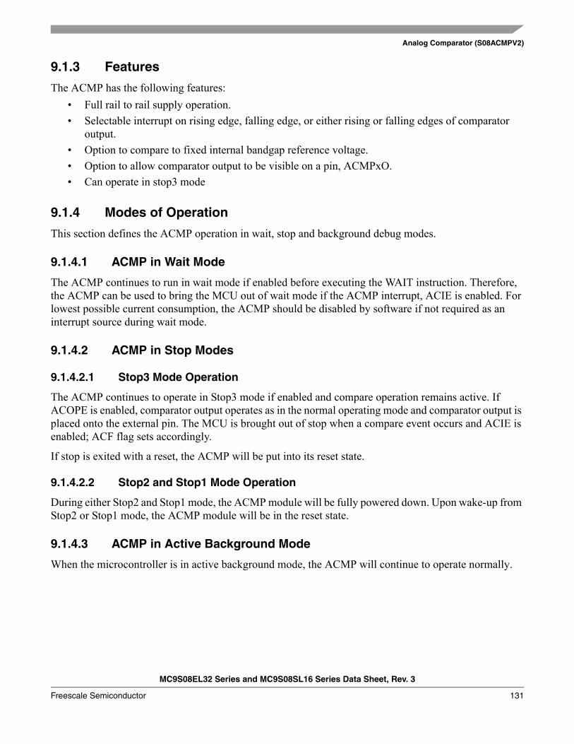
Analog Comparator (S08ACMPV2)
MC9S08EL32 Series and MC9S08SL16 Series Data Sheet, Rev. 3
Freescale Semiconductor 131
9.1.3 Features
The ACMP has the following features:• Full rail to rail supply operation.• Selectable interrupt on rising edge, falling edge, or either rising or falling edges of comparator
output.• Option to compare to fixed internal bandgap reference voltage.• Option to allow comparator output to be visible on a pin, ACMPxO.• Can operate in stop3 mode
9.1.4 Modes of Operation
This section defines the ACMP operation in wait, stop and background debug modes.
9.1.4.1 ACMP in Wait Mode
The ACMP continues to run in wait mode if enabled before executing the WAIT instruction. Therefore, the ACMP can be used to bring the MCU out of wait mode if the ACMP interrupt, ACIE is enabled. For lowest possible current consumption, the ACMP should be disabled by software if not required as an interrupt source during wait mode.
9.1.4.2 ACMP in Stop Modes
9.1.4.2.1 Stop3 Mode Operation
The ACMP continues to operate in Stop3 mode if enabled and compare operation remains active. If ACOPE is enabled, comparator output operates as in the normal operating mode and comparator output is placed onto the external pin. The MCU is brought out of stop when a compare event occurs and ACIE is enabled; ACF flag sets accordingly.
If stop is exited with a reset, the ACMP will be put into its reset state.
9.1.4.2.2 Stop2 and Stop1 Mode Operation
During either Stop2 and Stop1 mode, the ACMP module will be fully powered down. Upon wake-up from Stop2 or Stop1 mode, the ACMP module will be in the reset state.
9.1.4.3 ACMP in Active Background Mode
When the microcontroller is in active background mode, the ACMP will continue to operate normally.
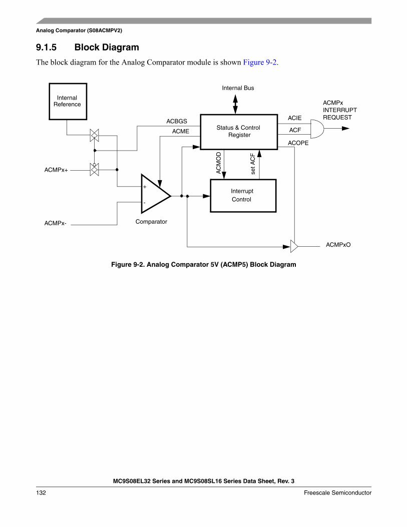
Analog Comparator (S08ACMPV2)
MC9S08EL32 Series and MC9S08SL16 Series Data Sheet, Rev. 3
132 Freescale Semiconductor
9.1.5 Block Diagram
The block diagram for the Analog Comparator module is shown Figure 9-2.
Figure 9-2. Analog Comparator 5V (ACMP5) Block Diagram
+
-
InterruptControl
InternalReference
ACBGS
Internal Bus
Status & Control Register
AC
MO
D
set A
CF
ACME ACF
ACIE
ACOPE
Comparator
ACMPxINTERRUPTREQUEST
ACMPx+
ACMPx-
ACMPxO
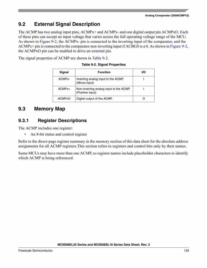
Analog Comparator (S08ACMPV2)
MC9S08EL32 Series and MC9S08SL16 Series Data Sheet, Rev. 3
Freescale Semiconductor 133
9.2 External Signal DescriptionThe ACMP has two analog input pins, ACMPx+ and ACMPx- and one digital output pin ACMPxO. Each of these pins can accept an input voltage that varies across the full operating voltage range of the MCU. As shown in Figure 9-2, the ACMPx- pin is connected to the inverting input of the comparator, and the ACMPx+ pin is connected to the comparator non-inverting input if ACBGS is a 0. As shown in Figure 9-2, the ACMPxO pin can be enabled to drive an external pin.
The signal properties of ACMP are shown in Table 9-2.
9.3 Memory Map
9.3.1 Register Descriptions
The ACMP includes one register:• An 8-bit status and control register
Refer to the direct-page register summary in the memory section of this data sheet for the absolute address assignments for all ACMP registers.This section refers to registers and control bits only by their names .
Some MCUs may have more than one ACMP, so register names include placeholder characters to identify which ACMP is being referenced.
Table 9-2. Signal Properties
Signal Function I/O
ACMPx- Inverting analog input to the ACMP.(Minus input)
I
ACMPx+ Non-inverting analog input to the ACMP.(Positive input)
I
ACMPxO Digital output of the ACMP. O
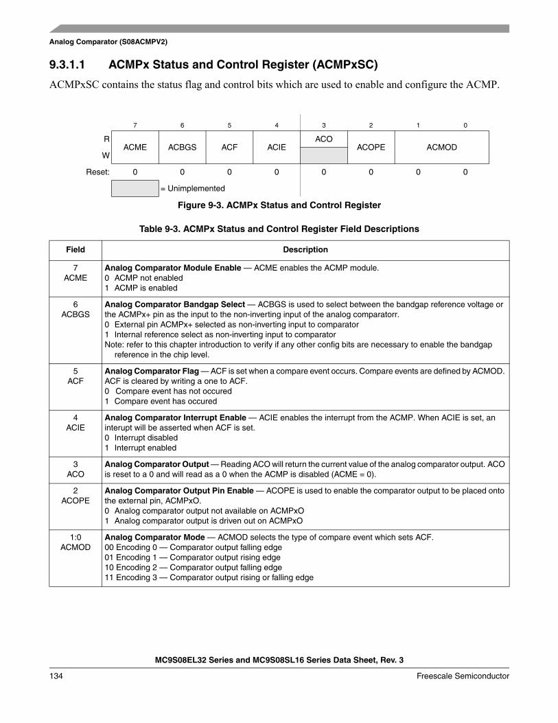
Analog Comparator (S08ACMPV2)
MC9S08EL32 Series and MC9S08SL16 Series Data Sheet, Rev. 3
134 Freescale Semiconductor
9.3.1.1 ACMPx Status and Control Register (ACMPxSC)
ACMPxSC contains the status flag and control bits which are used to enable and configure the ACMP.
7 6 5 4 3 2 1 0
RACME ACBGS ACF ACIE
ACOACOPE ACMOD
W
Reset: 0 0 0 0 0 0 0 0
= Unimplemented
Figure 9-3. ACMPx Status and Control Register
Table 9-3. ACMPx Status and Control Register Field Descriptions
Field Description
7ACME
Analog Comparator Module Enable — ACME enables the ACMP module.0 ACMP not enabled1 ACMP is enabled
6ACBGS
Analog Comparator Bandgap Select — ACBGS is used to select between the bandgap reference voltage or the ACMPx+ pin as the input to the non-inverting input of the analog comparatorr.0 External pin ACMPx+ selected as non-inverting input to comparator1 Internal reference select as non-inverting input to comparatorNote: refer to this chapter introduction to verify if any other config bits are necessary to enable the bandgap
reference in the chip level.
5ACF
Analog Comparator Flag — ACF is set when a compare event occurs. Compare events are defined by ACMOD. ACF is cleared by writing a one to ACF.0 Compare event has not occured1 Compare event has occured
4ACIE
Analog Comparator Interrupt Enable — ACIE enables the interrupt from the ACMP. When ACIE is set, an interupt will be asserted when ACF is set. 0 Interrupt disabled1 Interrupt enabled
3ACO
Analog Comparator Output — Reading ACO will return the current value of the analog comparator output. ACO is reset to a 0 and will read as a 0 when the ACMP is disabled (ACME = 0).
2ACOPE
Analog Comparator Output Pin Enable — ACOPE is used to enable the comparator output to be placed onto the external pin, ACMPxO. 0 Analog comparator output not available on ACMPxO1 Analog comparator output is driven out on ACMPxO
1:0ACMOD
Analog Comparator Mode — ACMOD selects the type of compare event which sets ACF. 00 Encoding 0 — Comparator output falling edge01 Encoding 1 — Comparator output rising edge10 Encoding 2 — Comparator output falling edge11 Encoding 3 — Comparator output rising or falling edge
Analog Comparator (S08ACMPV2)
MC9S08EL32 Series and MC9S08SL16 Series Data Sheet, Rev. 3
Freescale Semiconductor 135
9.4 Functional DescriptionThe analog comparator can be used to compare two analog input voltages applied to ACMPx+ and ACMPx-; or it can be used to compare an analog input voltage applied to ACMPx- with an internal bandgap reference voltage. ACBGS is used to select between the bandgap reference voltage or the ACMPx+ pin as the input to the non-inverting input of the analog comparator. The comparator output is high when the non-inverting input is greater than the inverting input, and is low when the non-inverting input is less than the inverting input. ACMOD is used to select the condition which will cause ACF to be set. ACF can be set on a rising edge of the comparator output, a falling edge of the comparator output, or either a rising or a falling edge (toggle). The comparator output can be read directly through ACO. The comparator output can be driven onto the ACMPxO pin using ACOPE.

Analog Comparator (S08ACMPV2)
MC9S08EL32 Series and MC9S08SL16 Series Data Sheet, Rev. 3
136 Freescale Semiconductor
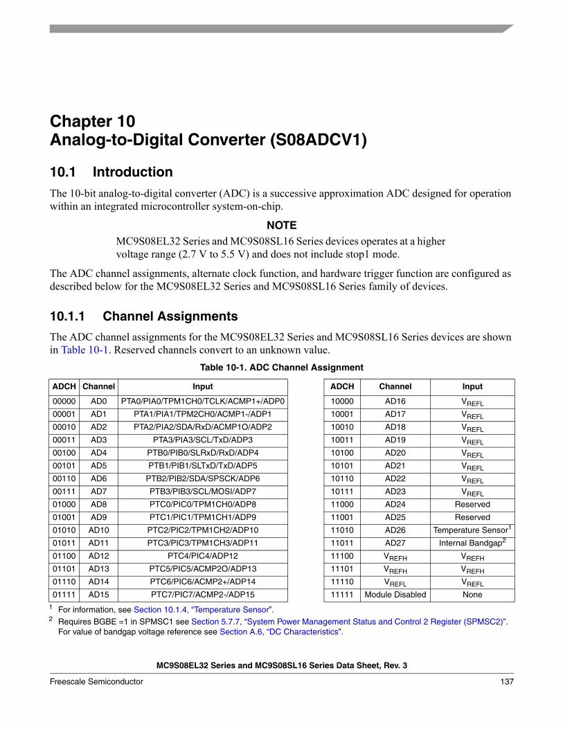
MC9S08EL32 Series and MC9S08SL16 Series Data Sheet, Rev. 3
Freescale Semiconductor 137
Chapter 10 Analog-to-Digital Converter (S08ADCV1)
10.1 IntroductionThe 10-bit analog-to-digital converter (ADC) is a successive approximation ADC designed for operation within an integrated microcontroller system-on-chip.
NOTEMC9S08EL32 Series and MC9S08SL16 Series devices operates at a higher voltage range (2.7 V to 5.5 V) and does not include stop1 mode.
The ADC channel assignments, alternate clock function, and hardware trigger function are configured as described below for the MC9S08EL32 Series and MC9S08SL16 Series family of devices.
10.1.1 Channel Assignments
The ADC channel assignments for the MC9S08EL32 Series and MC9S08SL16 Series devices are shown in Table 10-1. Reserved channels convert to an unknown value.
Table 10-1. ADC Channel Assignment
ADCH Channel Input ADCH Channel Input
00000 AD0 PTA0/PIA0/TPM1CH0/TCLK/ACMP1+/ADP0 10000 AD16 VREFL
00001 AD1 PTA1/PIA1/TPM2CH0/ACMP1-/ADP1 10001 AD17 VREFL
00010 AD2 PTA2/PIA2/SDA/RxD/ACMP1O/ADP2 10010 AD18 VREFL
00011 AD3 PTA3/PIA3/SCL/TxD/ADP3 10011 AD19 VREFL
00100 AD4 PTB0/PIB0/SLRxD/RxD/ADP4 10100 AD20 VREFL
00101 AD5 PTB1/PIB1/SLTxD/TxD/ADP5 10101 AD21 VREFL
00110 AD6 PTB2/PIB2/SDA/SPSCK/ADP6 10110 AD22 VREFL
00111 AD7 PTB3/PIB3/SCL/MOSI/ADP7 10111 AD23 VREFL
01000 AD8 PTC0/PIC0/TPM1CH0/ADP8 11000 AD24 Reserved
01001 AD9 PTC1/PIC1/TPM1CH1/ADP9 11001 AD25 Reserved
01010 AD10 PTC2/PIC2/TPM1CH2/ADP10 11010 AD26 Temperature Sensor1
1 For information, see Section 10.1.4, “Temperature Sensor”.
01011 AD11 PTC3/PIC3/TPM1CH3/ADP11 11011 AD27 Internal Bandgap2
2 Requires BGBE =1 in SPMSC1 see Section 5.7.7, “System Power Management Status and Control 2 Register (SPMSC2)”. For value of bandgap voltage reference see Section A.6, “DC Characteristics”.
01100 AD12 PTC4/PIC4/ADP12 11100 VREFH VREFH
01101 AD13 PTC5/PIC5/ACMP2O/ADP13 11101 VREFH VREFH
01110 AD14 PTC6/PIC6/ACMP2+/ADP14 11110 VREFL VREFL
01111 AD15 PTC7/PIC7/ACMP2-/ADP15 11111 Module Disabled None
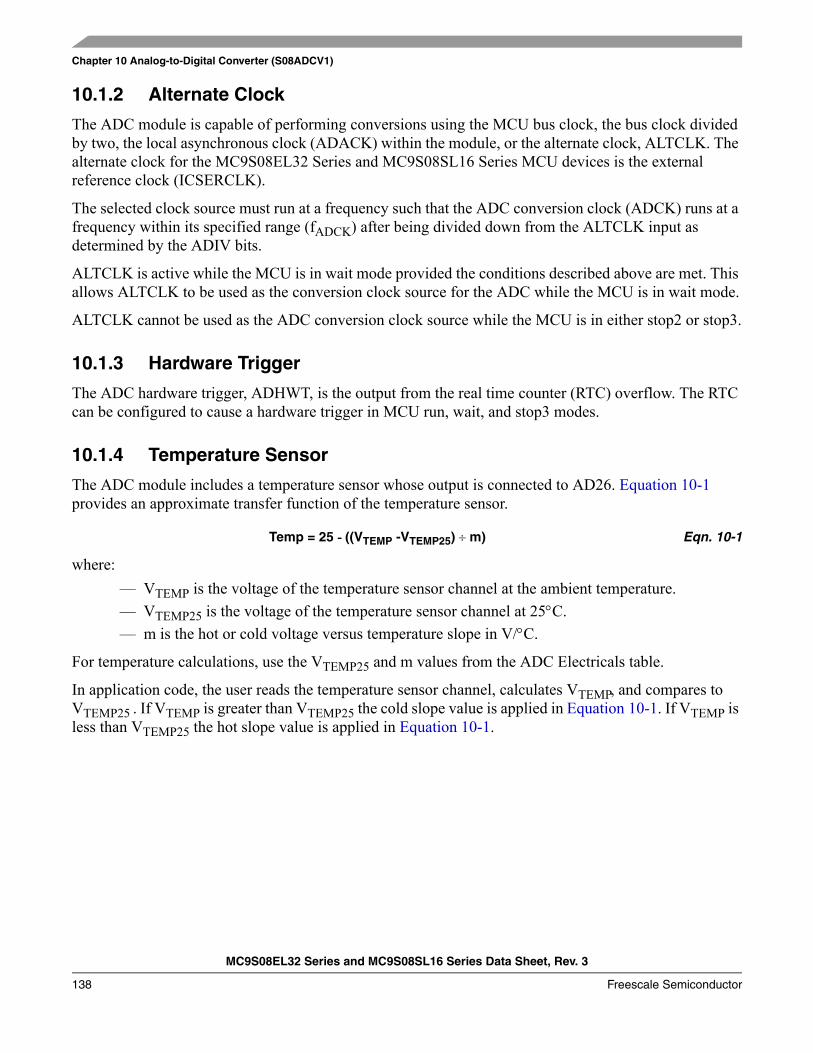
Chapter 10 Analog-to-Digital Converter (S08ADCV1)
MC9S08EL32 Series and MC9S08SL16 Series Data Sheet, Rev. 3
138 Freescale Semiconductor
10.1.2 Alternate Clock
The ADC module is capable of performing conversions using the MCU bus clock, the bus clock divided by two, the local asynchronous clock (ADACK) within the module, or the alternate clock, ALTCLK. The alternate clock for the MC9S08EL32 Series and MC9S08SL16 Series MCU devices is the external reference clock (ICSERCLK).
The selected clock source must run at a frequency such that the ADC conversion clock (ADCK) runs at a frequency within its specified range (fADCK) after being divided down from the ALTCLK input as determined by the ADIV bits.
ALTCLK is active while the MCU is in wait mode provided the conditions described above are met. This allows ALTCLK to be used as the conversion clock source for the ADC while the MCU is in wait mode.
ALTCLK cannot be used as the ADC conversion clock source while the MCU is in either stop2 or stop3.
10.1.3 Hardware Trigger
The ADC hardware trigger, ADHWT, is the output from the real time counter (RTC) overflow. The RTC can be configured to cause a hardware trigger in MCU run, wait, and stop3 modes.
10.1.4 Temperature Sensor
The ADC module includes a temperature sensor whose output is connected to AD26. Equation 10-1 provides an approximate transfer function of the temperature sensor.
Temp = 25 - ((VTEMP -VTEMP25) ÷ m) Eqn. 10-1
where:— VTEMP is the voltage of the temperature sensor channel at the ambient temperature. — VTEMP25 is the voltage of the temperature sensor channel at 25°C. — m is the hot or cold voltage versus temperature slope in V/°C.
For temperature calculations, use the VTEMP25 and m values from the ADC Electricals table.
In application code, the user reads the temperature sensor channel, calculates VTEMP, and compares to VTEMP25 . If VTEMP is greater than VTEMP25 the cold slope value is applied in Equation 10-1. If VTEMP is less than VTEMP25 the hot slope value is applied in Equation 10-1.
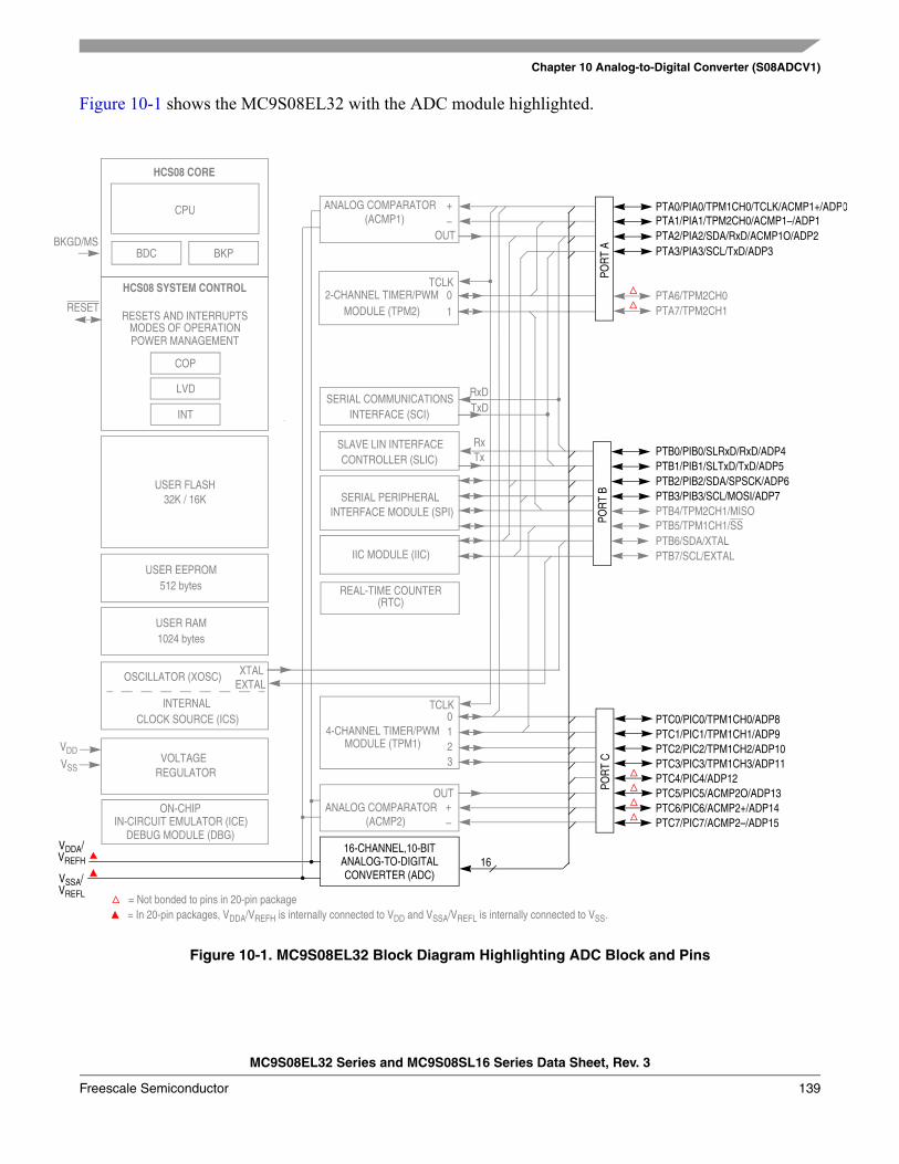
Chapter 10 Analog-to-Digital Converter (S08ADCV1)
MC9S08EL32 Series and MC9S08SL16 Series Data Sheet, Rev. 3
Freescale Semiconductor 139
Figure 10-1 shows the MC9S08EL32 with the ADC module highlighted.
Figure 10-1. MC9S08EL32 Block Diagram Highlighting ADC Block and Pins
VSS
IIC MODULE (IIC)
SERIAL PERIPHERAL INTERFACE MODULE (SPI)
USER FLASH
USER RAM
32K / 16K
HCS08 CORE
CPU
BDC
2-CHANNEL TIMER/PWMMODULE (TPM2)
HCS08 SYSTEM CONTROL
RESETS AND INTERRUPTSMODES OF OPERATIONPOWER MANAGEMENT
VOLTAGE REGULATOR
COP
LVD
OSCILLATOR (XOSC)
INTERNALCLOCK SOURCE (ICS)
RESET
VREFH
1024 bytes
INTERFACE (SCI)SERIAL COMMUNICATIONS
XTALEXTAL
4-CHANNEL TIMER/PWMMODULE (TPM1)
REAL-TIME COUNTER
IN-CIRCUIT EMULATOR (ICE)
BKGD/MS PTA3/PIA3/SCL/TxD/ADP3
PTA6/TPM2CH0
PTA2/PIA2/SDA/RxD/ACMP1O/ADP2PTA1/PIA1/TPM2CH0/ACMP1–/ADP1PTA0/PIA0/TPM1CH0/TCLK/ACMP1+/ADP0
PTA7/TPM2CH1
PTB3/PIB3/SCL/MOSI/ADP7PTB4/TPM2CH1/MISO
PTB2/PIB2/SDA/SPSCK/ADP6PTB1/PIB1/SLTxD/TxD/ADP5PTB0/PIB0/SLRxD/RxD/ADP4
PTB7/SCL/EXTAL
PTC3/PIC3/TPM1CH3/ADP11PTC4/PIC4/ADP12PTC5/PIC5/ACMP2O/ADP13
PTC2/PIC2/TPM1CH2/ADP10PTC1/PIC1/TPM1CH1/ADP9
POR
T C
PTC6/PIC6/ACMP2+/ADP14
VDD
BKP
INT
ANALOG COMPARATOR(ACMP2)
USER EEPROM512 bytes
CONTROLLER (SLIC)SLAVE LIN INTERFACE
ANALOG-TO-DIGITALCONVERTER (ADC)
16-CHANNEL,10-BIT16
= In 20-pin packages, VDDA/VREFH is internally connected to VDD and VSSA/VREFL is internally connected to VSS.
VDDA/
VREFL
VSSA/
DEBUG MODULE (DBG)
ON-CHIP
(RTC)
PTC0/PIC0/TPM1CH0/ADP8
PTC7/PIC7/ACMP2–/ADP15
PTB6/SDA/XTAL
POR
T B
POR
T A
PTB5/TPM1CH1/SS
ANALOG COMPARATOR(ACMP1)
= Not bonded to pins in 20-pin package
TCLK
TCLK
+–
OUT
+–
OUT
0123
10
RxDTxD
TxRx

Chapter 10 Analog-to-Digital Converter (S08ADCV1)
MC9S08EL32 Series and MC9S08SL16 Series Data Sheet, Rev. 3
140 Freescale Semiconductor
Analog-to-Digital Converter (S08ADC10V1)
MC9S08EL32 Series and MC9S08SL16 Series Data Sheet, Rev. 3
Freescale Semiconductor 141
10.1.5 Features
Features of the ADC module include:• Linear successive approximation algorithm with 10 bits resolution.• Up to 28 analog inputs.• Output formatted in 10- or 8-bit right-justified format.• Single or continuous conversion (automatic return to idle after single conversion).• Configurable sample time and conversion speed/power.• Conversion complete flag and interrupt.• Input clock selectable from up to four sources.• Operation in wait or stop3 modes for lower noise operation.• Asynchronous clock source for lower noise operation.• Selectable asynchronous hardware conversion trigger.• Automatic compare with interrupt for less-than, or greater-than or equal-to, programmable value.
10.1.6 Block Diagram
Figure 10-2 provides a block diagram of the ADC module
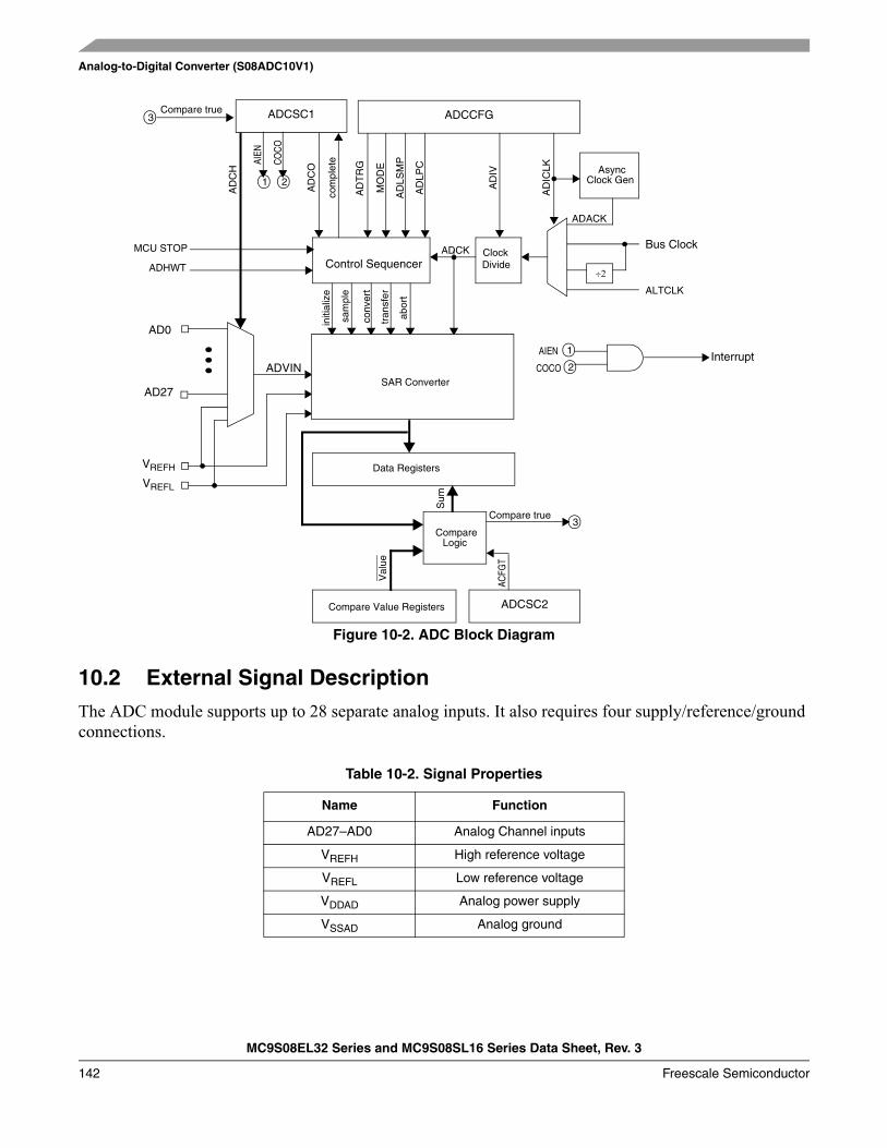
Analog-to-Digital Converter (S08ADC10V1)
MC9S08EL32 Series and MC9S08SL16 Series Data Sheet, Rev. 3
142 Freescale Semiconductor
Figure 10-2. ADC Block Diagram
10.2 External Signal DescriptionThe ADC module supports up to 28 separate analog inputs. It also requires four supply/reference/ground connections.
Table 10-2. Signal Properties
Name Function
AD27–AD0 Analog Channel inputs
VREFH High reference voltage
VREFL Low reference voltage
VDDAD Analog power supply
VSSAD Analog ground
AD0
• • •
AD27
VREFH
VREFL
ADVIN
AD
CH
Control Sequencer
initi
aliz
e
sam
ple
conv
ert
tran
sfer
abor
t
ClockDivide
ADCK
÷2
AsyncClock Gen
Bus Clock
ALTCLK
AD
ICLK
AD
IV
ADACK
AD
CO
AD
LSM
P
AD
LPC
MO
DE
com
plet
e
Data Registers
SAR Converter
Compare Value Registers
Compare
Val
ue
Sum
AIEN
CO
CO
InterruptAIEN
COCOA
DT
RG
1
2
1 2
MCU STOP
ADHWT
Logic
ACFG
T
3Compare true
3Compare true ADCCFGADCSC1
ADCSC2
Analog-to-Digital Converter (S08ADC10V1)
MC9S08EL32 Series and MC9S08SL16 Series Data Sheet, Rev. 3
Freescale Semiconductor 143
10.2.1 Analog Power (VDDAD)
The ADC analog portion uses VDDAD as its power connection. In some packages, VDDAD is connected internally to VDD. If externally available, connect the VDDAD pin to the same voltage potential as VDD. External filtering may be necessary to ensure clean VDDAD for good results.
10.2.2 Analog Ground (VSSAD)
The ADC analog portion uses VSSAD as its ground connection. In some packages, VSSAD is connected internally to VSS. If externally available, connect the VSSAD pin to the same voltage potential as VSS.
10.2.3 Voltage Reference High (VREFH)
VREFH is the high reference voltage for the converter. In some packages, VREFH is connected internally to VDDAD. If externally available, VREFH may be connected to the same potential as VDDAD, or may be driven by an external source that is between the minimum VDDAD spec and the VDDAD potential (VREFH must never exceed VDDAD).
10.2.4 Voltage Reference Low (VREFL)
VREFL is the low reference voltage for the converter. In some packages, VREFL is connected internally to VSSAD. If externally available, connect the VREFL pin to the same voltage potential as VSSAD.
10.2.5 Analog Channel Inputs (ADx)
The ADC module supports up to 28 separate analog inputs. An input is selected for conversion through the ADCH channel select bits.
10.3 Register Definition
These memory mapped registers control and monitor operation of the ADC:
• Status and control register, ADCSC1• Status and control register, ADCSC2• Data result registers, ADCRH and ADCRL• Compare value registers, ADCCVH and ADCCVL• Configuration register, ADCCFG• Pin enable registers, APCTL1, APCTL2, APCTL3
10.3.1 Status and Control Register 1 (ADCSC1)
This section describes the function of the ADC status and control register (ADCSC1). Writing ADCSC1 aborts the current conversion and initiates a new conversion (if the ADCH bits are equal to a value other than all 1s).
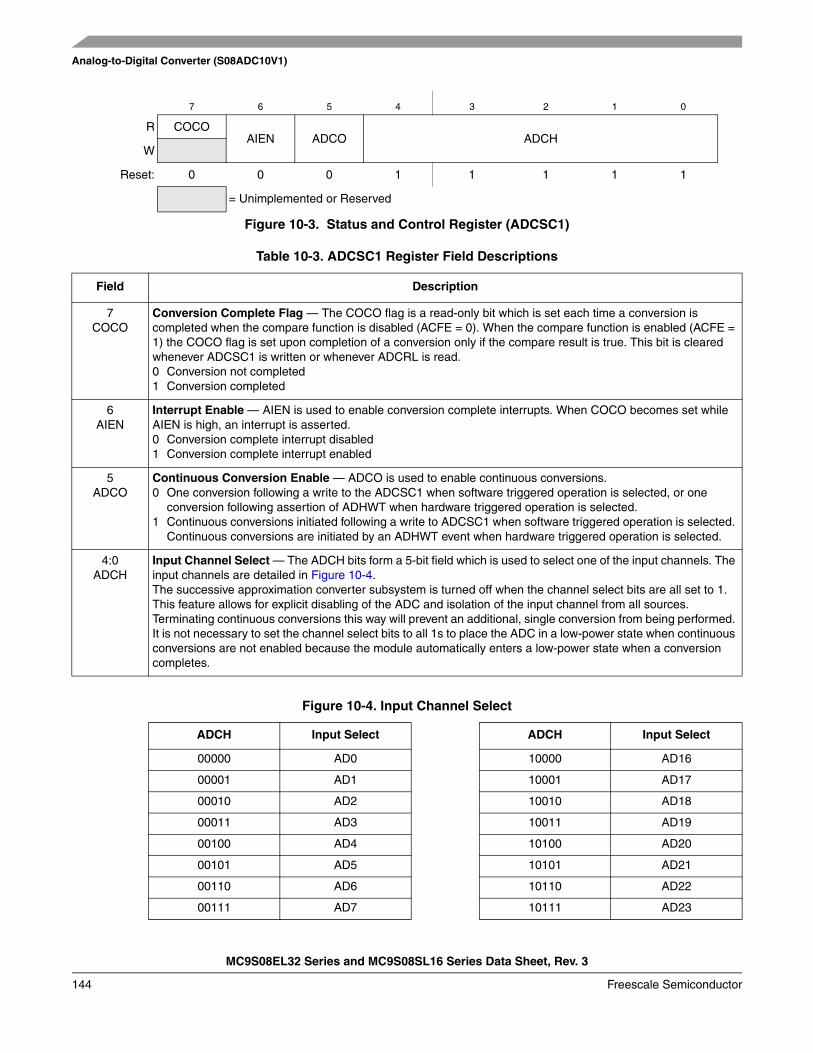
Analog-to-Digital Converter (S08ADC10V1)
MC9S08EL32 Series and MC9S08SL16 Series Data Sheet, Rev. 3
144 Freescale Semiconductor
7 6 5 4 3 2 1 0
R COCOAIEN ADCO ADCH
W
Reset: 0 0 0 1 1 1 1 1
= Unimplemented or Reserved
Figure 10-3. Status and Control Register (ADCSC1)
Table 10-3. ADCSC1 Register Field Descriptions
Field Description
7COCO
Conversion Complete Flag — The COCO flag is a read-only bit which is set each time a conversion is completed when the compare function is disabled (ACFE = 0). When the compare function is enabled (ACFE = 1) the COCO flag is set upon completion of a conversion only if the compare result is true. This bit is cleared whenever ADCSC1 is written or whenever ADCRL is read.0 Conversion not completed1 Conversion completed
6AIEN
Interrupt Enable — AIEN is used to enable conversion complete interrupts. When COCO becomes set while AIEN is high, an interrupt is asserted.0 Conversion complete interrupt disabled1 Conversion complete interrupt enabled
5ADCO
Continuous Conversion Enable — ADCO is used to enable continuous conversions.0 One conversion following a write to the ADCSC1 when software triggered operation is selected, or one
conversion following assertion of ADHWT when hardware triggered operation is selected.1 Continuous conversions initiated following a write to ADCSC1 when software triggered operation is selected.
Continuous conversions are initiated by an ADHWT event when hardware triggered operation is selected.
4:0ADCH
Input Channel Select — The ADCH bits form a 5-bit field which is used to select one of the input channels. The input channels are detailed in Figure 10-4.The successive approximation converter subsystem is turned off when the channel select bits are all set to 1. This feature allows for explicit disabling of the ADC and isolation of the input channel from all sources. Terminating continuous conversions this way will prevent an additional, single conversion from being performed. It is not necessary to set the channel select bits to all 1s to place the ADC in a low-power state when continuous conversions are not enabled because the module automatically enters a low-power state when a conversion completes.
Figure 10-4. Input Channel Select
ADCH Input Select ADCH Input Select
00000 AD0 10000 AD16
00001 AD1 10001 AD17
00010 AD2 10010 AD18
00011 AD3 10011 AD19
00100 AD4 10100 AD20
00101 AD5 10101 AD21
00110 AD6 10110 AD22
00111 AD7 10111 AD23
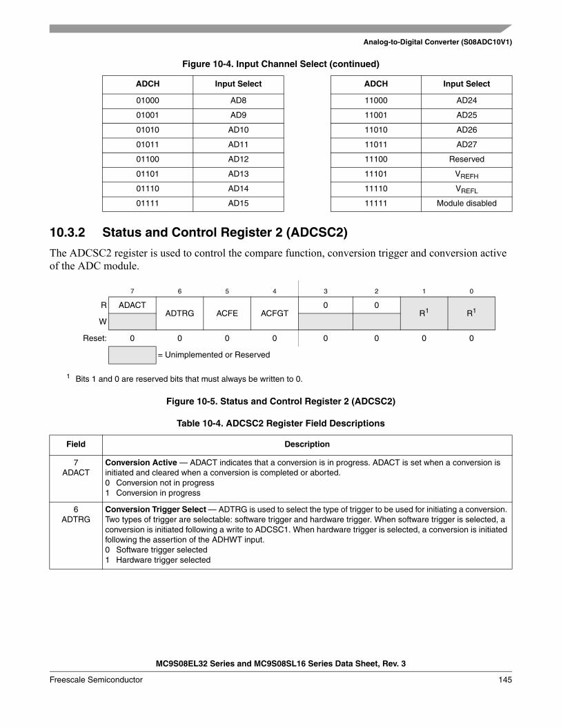
Analog-to-Digital Converter (S08ADC10V1)
MC9S08EL32 Series and MC9S08SL16 Series Data Sheet, Rev. 3
Freescale Semiconductor 145
10.3.2 Status and Control Register 2 (ADCSC2)
The ADCSC2 register is used to control the compare function, conversion trigger and conversion active of the ADC module.
Figure 10-5. Status and Control Register 2 (ADCSC2)
01000 AD8 11000 AD24
01001 AD9 11001 AD25
01010 AD10 11010 AD26
01011 AD11 11011 AD27
01100 AD12 11100 Reserved
01101 AD13 11101 VREFH
01110 AD14 11110 VREFL
01111 AD15 11111 Module disabled
7 6 5 4 3 2 1 0
R ADACTADTRG ACFE ACFGT
0 0R1
1 Bits 1 and 0 are reserved bits that must always be written to 0.
R1
W
Reset: 0 0 0 0 0 0 0 0
= Unimplemented or Reserved
Table 10-4. ADCSC2 Register Field Descriptions
Field Description
7ADACT
Conversion Active — ADACT indicates that a conversion is in progress. ADACT is set when a conversion is initiated and cleared when a conversion is completed or aborted.0 Conversion not in progress1 Conversion in progress
6ADTRG
Conversion Trigger Select — ADTRG is used to select the type of trigger to be used for initiating a conversion. Two types of trigger are selectable: software trigger and hardware trigger. When software trigger is selected, a conversion is initiated following a write to ADCSC1. When hardware trigger is selected, a conversion is initiated following the assertion of the ADHWT input.0 Software trigger selected1 Hardware trigger selected
Figure 10-4. Input Channel Select (continued)
ADCH Input Select ADCH Input Select
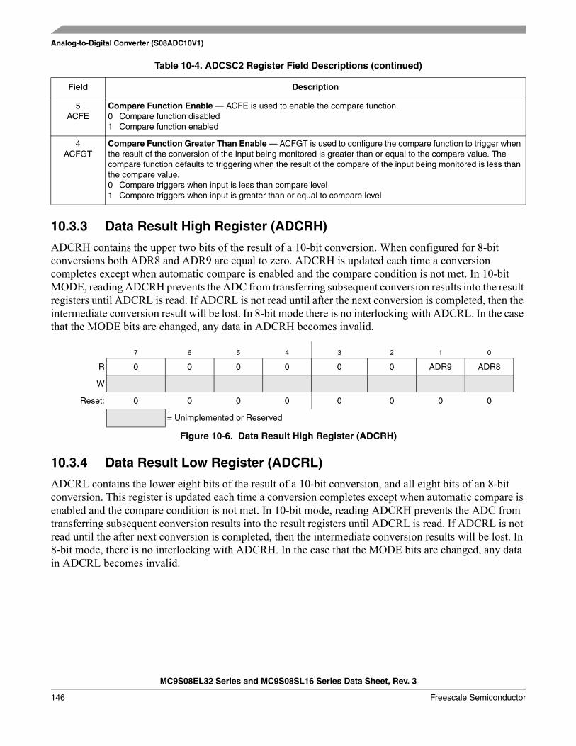
Analog-to-Digital Converter (S08ADC10V1)
MC9S08EL32 Series and MC9S08SL16 Series Data Sheet, Rev. 3
146 Freescale Semiconductor
10.3.3 Data Result High Register (ADCRH)
ADCRH contains the upper two bits of the result of a 10-bit conversion. When configured for 8-bit conversions both ADR8 and ADR9 are equal to zero. ADCRH is updated each time a conversion completes except when automatic compare is enabled and the compare condition is not met. In 10-bit MODE, reading ADCRH prevents the ADC from transferring subsequent conversion results into the result registers until ADCRL is read. If ADCRL is not read until after the next conversion is completed, then the intermediate conversion result will be lost. In 8-bit mode there is no interlocking with ADCRL. In the case that the MODE bits are changed, any data in ADCRH becomes invalid.
10.3.4 Data Result Low Register (ADCRL)
ADCRL contains the lower eight bits of the result of a 10-bit conversion, and all eight bits of an 8-bit conversion. This register is updated each time a conversion completes except when automatic compare is enabled and the compare condition is not met. In 10-bit mode, reading ADCRH prevents the ADC from transferring subsequent conversion results into the result registers until ADCRL is read. If ADCRL is not read until the after next conversion is completed, then the intermediate conversion results will be lost. In 8-bit mode, there is no interlocking with ADCRH. In the case that the MODE bits are changed, any data in ADCRL becomes invalid.
5ACFE
Compare Function Enable — ACFE is used to enable the compare function.0 Compare function disabled1 Compare function enabled
4ACFGT
Compare Function Greater Than Enable — ACFGT is used to configure the compare function to trigger when the result of the conversion of the input being monitored is greater than or equal to the compare value. The compare function defaults to triggering when the result of the compare of the input being monitored is less than the compare value.0 Compare triggers when input is less than compare level1 Compare triggers when input is greater than or equal to compare level
7 6 5 4 3 2 1 0
R 0 0 0 0 0 0 ADR9 ADR8
W
Reset: 0 0 0 0 0 0 0 0
= Unimplemented or Reserved
Figure 10-6. Data Result High Register (ADCRH)
Table 10-4. ADCSC2 Register Field Descriptions (continued)
Field Description
Analog-to-Digital Converter (S08ADC10V1)
MC9S08EL32 Series and MC9S08SL16 Series Data Sheet, Rev. 3
Freescale Semiconductor 147
10.3.5 Compare Value High Register (ADCCVH)
This register holds the upper two bits of the 10-bit compare value. These bits are compared to the upper two bits of the result following a conversion in 10-bit mode when the compare function is enabled.In 8-bit operation, ADCCVH is not used during compare.
10.3.6 Compare Value Low Register (ADCCVL)
This register holds the lower 8 bits of the 10-bit compare value, or all 8 bits of the 8-bit compare value. Bits ADCV7:ADCV0 are compared to the lower 8 bits of the result following a conversion in either 10-bit or 8-bit mode.
10.3.7 Configuration Register (ADCCFG)
ADCCFG is used to select the mode of operation, clock source, clock divide, and configure for low power or long sample time.
7 6 5 4 3 2 1 0
R ADR7 ADR6 ADR5 ADR4 ADR3 ADR2 ADR1 ADR0
W
Reset: 0 0 0 0 0 0 0 0
= Unimplemented or Reserved
Figure 10-7. Data Result Low Register (ADCRL)
7 6 5 4 3 2 1 0
R 0 0 0 0ADCV9 ADCV8
W
Reset: 0 0 0 0 0 0 0 0
= Unimplemented or Reserved
Figure 10-8. Compare Value High Register (ADCCVH)
7 6 5 4 3 2 1 0
RADCV7 ADCV6 ADCV5 ADCV4 ADCV3 ADCV2 ADCV1 ADCV0
W
Reset: 0 0 0 0 0 0 0 0
Figure 10-9. Compare Value Low Register(ADCCVL)
Analog-to-Digital Converter (S08ADC10V1)
MC9S08EL32 Series and MC9S08SL16 Series Data Sheet, Rev. 3
148 Freescale Semiconductor
7 6 5 4 3 2 1 0
RADLPC ADIV ADLSMP MODE ADICLK
W
Reset: 0 0 0 0 0 0 0 0
Figure 10-10. Configuration Register (ADCCFG)
Table 10-5. ADCCFG Register Field Descriptions
Field Description
7ADLPC
Low Power Configuration — ADLPC controls the speed and power configuration of the successive approximation converter. This is used to optimize power consumption when higher sample rates are not required.0 High speed configuration1 Low power configuration: {FC31}The power is reduced at the expense of maximum clock speed.
6:5ADIV
Clock Divide Select — ADIV select the divide ratio used by the ADC to generate the internal clock ADCK. Table 10-6 shows the available clock configurations.
4ADLSMP
Long Sample Time Configuration — ADLSMP selects between long and short sample time. This adjusts the sample period to allow higher impedance inputs to be accurately sampled or to maximize conversion speed for lower impedance inputs. Longer sample times can also be used to lower overall power consumption when continuous conversions are enabled if high conversion rates are not required.0 Short sample time1 Long sample time
3:2MODE
Conversion Mode Selection — MODE bits are used to select between 10- or 8-bit operation. See Table 10-7.
1:0ADICLK
Input Clock Select — ADICLK bits select the input clock source to generate the internal clock ADCK. See Table 10-8.
Table 10-6. Clock Divide Select
ADIV Divide Ratio Clock Rate
00 1 Input clock
01 2 Input clock ÷ 2
10 4 Input clock ÷ 4
11 8 Input clock ÷ 8
Table 10-7. Conversion Modes
MODE Mode Description
00 8-bit conversion (N=8)
01 Reserved
10 10-bit conversion (N=10)
11 Reserved
Analog-to-Digital Converter (S08ADC10V1)
MC9S08EL32 Series and MC9S08SL16 Series Data Sheet, Rev. 3
Freescale Semiconductor 149
10.3.8 Pin Control 1 Register (APCTL1)The pin control registers are used to disable the I/O port control of MCU pins used as analog inputs. APCTL1 is used to control the pins associated with channels 0–7 of the ADC module.
Table 10-8. Input Clock Select
ADICLK Selected Clock Source
00 Bus clock
01 Bus clock divided by 2
10 Alternate clock (ALTCLK)
11 Asynchronous clock (ADACK)
7 6 5 4 3 2 1 0
RADPC7 ADPC6 ADPC5 ADPC4 ADPC3 ADPC2 ADPC1 ADPC0
W
Reset: 0 0 0 0 0 0 0 0
Figure 10-11. Pin Control 1 Register (APCTL1)
Table 10-9. APCTL1 Register Field Descriptions
Field Description
7ADPC7
ADC Pin Control 7 — ADPC7 is used to control the pin associated with channel AD7.0 AD7 pin I/O control enabled1 AD7 pin I/O control disabled
6ADPC6
ADC Pin Control 6 — ADPC6 is used to control the pin associated with channel AD6.0 AD6 pin I/O control enabled1 AD6 pin I/O control disabled
5ADPC5
ADC Pin Control 5 — ADPC5 is used to control the pin associated with channel AD5.0 AD5 pin I/O control enabled1 AD5 pin I/O control disabled
4ADPC4
ADC Pin Control 4 — ADPC4 is used to control the pin associated with channel AD4.0 AD4 pin I/O control enabled1 AD4 pin I/O control disabled
3ADPC3
ADC Pin Control 3 — ADPC3 is used to control the pin associated with channel AD3.0 AD3 pin I/O control enabled1 AD3 pin I/O control disabled
2ADPC2
ADC Pin Control 2 — ADPC2 is used to control the pin associated with channel AD2.0 AD2 pin I/O control enabled1 AD2 pin I/O control disabled
Analog-to-Digital Converter (S08ADC10V1)
MC9S08EL32 Series and MC9S08SL16 Series Data Sheet, Rev. 3
150 Freescale Semiconductor
10.3.9 Pin Control 2 Register (APCTL2)
APCTL2 is used to control channels 8–15 of the ADC module.
1ADPC1
ADC Pin Control 1 — ADPC1 is used to control the pin associated with channel AD1.0 AD1 pin I/O control enabled1 AD1 pin I/O control disabled
0ADPC0
ADC Pin Control 0 — ADPC0 is used to control the pin associated with channel AD0.0 AD0 pin I/O control enabled1 AD0 pin I/O control disabled
7 6 5 4 3 2 1 0
RADPC15 ADPC14 ADPC13 ADPC12 ADPC11 ADPC10 ADPC9 ADPC8
W
Reset: 0 0 0 0 0 0 0 0
Figure 10-12. Pin Control 2 Register (APCTL2)
Table 10-10. APCTL2 Register Field Descriptions
Field Description
7ADPC15
ADC Pin Control 15 — ADPC15 is used to control the pin associated with channel AD15.0 AD15 pin I/O control enabled1 AD15 pin I/O control disabled
6ADPC14
ADC Pin Control 14 — ADPC14 is used to control the pin associated with channel AD14.0 AD14 pin I/O control enabled1 AD14 pin I/O control disabled
5ADPC13
ADC Pin Control 13 — ADPC13 is used to control the pin associated with channel AD13.0 AD13 pin I/O control enabled1 AD13 pin I/O control disabled
4ADPC12
ADC Pin Control 12 — ADPC12 is used to control the pin associated with channel AD12.0 AD12 pin I/O control enabled1 AD12 pin I/O control disabled
3ADPC11
ADC Pin Control 11 — ADPC11 is used to control the pin associated with channel AD11.0 AD11 pin I/O control enabled1 AD11 pin I/O control disabled
2ADPC10
ADC Pin Control 10 — ADPC10 is used to control the pin associated with channel AD10.0 AD10 pin I/O control enabled1 AD10 pin I/O control disabled
Table 10-9. APCTL1 Register Field Descriptions (continued)
Field Description
Analog-to-Digital Converter (S08ADC10V1)
MC9S08EL32 Series and MC9S08SL16 Series Data Sheet, Rev. 3
Freescale Semiconductor 151
10.3.10 Pin Control 3 Register (APCTL3)
APCTL3 is used to control channels 16–23 of the ADC module.
1ADPC9
ADC Pin Control 9 — ADPC9 is used to control the pin associated with channel AD9. 0 AD9 pin I/O control enabled1 AD9 pin I/O control disabled
0ADPC8
ADC Pin Control 8 — ADPC8 is used to control the pin associated with channel AD8. 0 AD8 pin I/O control enabled1 AD8 pin I/O control disabled
7 6 5 4 3 2 1 0
RADPC23 ADPC22 ADPC21 ADPC20 ADPC19 ADPC18 ADPC17 ADPC16
W
Reset: 0 0 0 0 0 0 0 0
Figure 10-13. Pin Control 3 Register (APCTL3)
Table 10-11. APCTL3 Register Field Descriptions
Field Description
7ADPC23
ADC Pin Control 23 — ADPC23 is used to control the pin associated with channel AD23. 0 AD23 pin I/O control enabled1 AD23 pin I/O control disabled
6ADPC22
ADC Pin Control 22 — ADPC22 is used to control the pin associated with channel AD22. 0 AD22 pin I/O control enabled1 AD22 pin I/O control disabled
5ADPC21
ADC Pin Control 21 — ADPC21 is used to control the pin associated with channel AD21. 0 AD21 pin I/O control enabled1 AD21 pin I/O control disabled
4ADPC20
ADC Pin Control 20 — ADPC20 is used to control the pin associated with channel AD20. 0 AD20 pin I/O control enabled1 AD20 pin I/O control disabled
3ADPC19
ADC Pin Control 19 — ADPC19 is used to control the pin associated with channel AD19. 0 AD19 pin I/O control enabled1 AD19 pin I/O control disabled
2ADPC18
ADC Pin Control 18 — ADPC18 is used to control the pin associated with channel AD18. 0 AD18 pin I/O control enabled1 AD18 pin I/O control disabled
Table 10-10. APCTL2 Register Field Descriptions (continued)
Field Description
Analog-to-Digital Converter (S08ADC10V1)
MC9S08EL32 Series and MC9S08SL16 Series Data Sheet, Rev. 3
152 Freescale Semiconductor
10.4 Functional DescriptionThe ADC module is disabled during reset or when the ADCH bits are all high. The module is idle when a conversion has completed and another conversion has not been initiated. When idle, the module is in its lowest power state.
The ADC can perform an analog-to-digital conversion on any of the software selectable channels. The selected channel voltage is converted by a successive approximation algorithm into an 11-bit digital result. In 8-bit mode, the selected channel voltage is converted by a successive approximation algorithm into a 9-bit digital result.
When the conversion is completed, the result is placed in the data registers (ADCRH and ADCRL).In 10-bit mode, the result is rounded to 10 bits and placed in ADCRH and ADCRL. In 8-bit mode, the result is rounded to 8 bits and placed in ADCRL. The conversion complete flag (COCO) is then set and an interrupt is generated if the conversion complete interrupt has been enabled (AIEN = 1).
The ADC module has the capability of automatically comparing the result of a conversion with the contents of its compare registers. The compare function is enabled by setting the ACFE bit and operates in conjunction with any of the conversion modes and configurations.
10.4.1 Clock Select and Divide Control
One of four clock sources can be selected as the clock source for the ADC module. This clock source is then divided by a configurable value to generate the input clock to the converter (ADCK). The clock is selected from one of the following sources by means of the ADICLK bits.
• The bus clock, which is equal to the frequency at which software is executed. This is the default selection following reset.
• The bus clock divided by 2. For higher bus clock rates, this allows a maximum divide by 16 of the bus clock.
• ALTCLK, as defined for this MCU (See module section introduction).• The asynchronous clock (ADACK) – This clock is generated from a clock source within the ADC
module. When selected as the clock source this clock remains active while the MCU is in wait or stop3 mode and allows conversions in these modes for lower noise operation.
Whichever clock is selected, its frequency must fall within the specified frequency range for ADCK. If the available clocks are too slow, the ADC will not perform according to specifications. If the available clocks
1ADPC17
ADC Pin Control 17 — ADPC17 is used to control the pin associated with channel AD17. 0 AD17 pin I/O control enabled1 AD17 pin I/O control disabled
0ADPC16
ADC Pin Control 16 — ADPC16 is used to control the pin associated with channel AD16. 0 AD16 pin I/O control enabled1 AD16 pin I/O control disabled
Table 10-11. APCTL3 Register Field Descriptions (continued)
Field Description
Analog-to-Digital Converter (S08ADC10V1)
MC9S08EL32 Series and MC9S08SL16 Series Data Sheet, Rev. 3
Freescale Semiconductor 153
are too fast, then the clock must be divided to the appropriate frequency. This divider is specified by the ADIV bits and can be divide-by 1, 2, 4, or 8.
10.4.2 Input Select and Pin Control
The pin control registers (APCTL3, APCTL2, and APCTL1) are used to disable the I/O port control of the pins used as analog inputs.When a pin control register bit is set, the following conditions are forced for the associated MCU pin:
• The output buffer is forced to its high impedance state.• The input buffer is disabled. A read of the I/O port returns a zero for any pin with its input buffer
disabled.• The pullup is disabled.
10.4.3 Hardware Trigger
The ADC module has a selectable asynchronous hardware conversion trigger, ADHWT, that is enabled when the ADTRG bit is set. This source is not available on all MCUs. Consult the module introduction for information on the ADHWT source specific to this MCU.
When ADHWT source is available and hardware trigger is enabled (ADTRG=1), a conversion is initiated on the rising edge of ADHWT. If a conversion is in progress when a rising edge occurs, the rising edge is ignored. In continuous convert configuration, only the initial rising edge to launch continuous conversions is observed. The hardware trigger function operates in conjunction with any of the conversion modes and configurations.
10.4.4 Conversion Control
Conversions can be performed in either 10-bit mode or 8-bit mode as determined by the MODE bits. Conversions can be initiated by either a software or hardware trigger. In addition, the ADC module can be configured for low power operation, long sample time, continuous conversion, and automatic compare of the conversion result to a software determined compare value.
10.4.4.1 Initiating Conversions
A conversion is initiated:• Following a write to ADCSC1 (with ADCH bits not all 1s) if software triggered operation is
selected.• Following a hardware trigger (ADHWT) event if hardware triggered operation is selected.• Following the transfer of the result to the data registers when continuous conversion is enabled.
If continuous conversions are enabled a new conversion is automatically initiated after the completion of the current conversion. In software triggered operation, continuous conversions begin after ADCSC1 is written and continue until aborted. In hardware triggered operation, continuous conversions begin after a hardware trigger event and continue until aborted.
Analog-to-Digital Converter (S08ADC10V1)
MC9S08EL32 Series and MC9S08SL16 Series Data Sheet, Rev. 3
154 Freescale Semiconductor
10.4.4.2 Completing Conversions
A conversion is completed when the result of the conversion is transferred into the data result registers, ADCRH and ADCRL. This is indicated by the setting of COCO. An interrupt is generated if AIEN is high at the time that COCO is set.
A blocking mechanism prevents a new result from overwriting previous data in ADCRH and ADCRL if the previous data is in the process of being read while in 10-bit MODE (the ADCRH register has been read but the ADCRL register has not). When blocking is active, the data transfer is blocked, COCO is not set, and the new result is lost. In the case of single conversions with the compare function enabled and the compare condition false, blocking has no effect and ADC operation is terminated. In all other cases of operation, when a data transfer is blocked, another conversion is initiated regardless of the state of ADCO (single or continuous conversions enabled).
If single conversions are enabled, the blocking mechanism could result in several discarded conversions and excess power consumption. To avoid this issue, the data registers must not be read after initiating a single conversion until the conversion completes.
10.4.4.3 Aborting Conversions
Any conversion in progress will be aborted when:
• A write to ADCSC1 occurs (the current conversion will be aborted and a new conversion will be initiated, if ADCH are not all 1s).
• A write to ADCSC2, ADCCFG, ADCCVH, or ADCCVL occurs. This indicates a mode of operation change has occurred and the current conversion is therefore invalid.
• The MCU is reset.
• The MCU enters stop mode with ADACK not enabled.
When a conversion is aborted, the contents of the data registers, ADCRH and ADCRL, are not altered but continue to be the values transferred after the completion of the last successful conversion. In the case that the conversion was aborted by a reset, ADCRH and ADCRL return to their reset states.
10.4.4.4 Power Control
The ADC module remains in its idle state until a conversion is initiated. If ADACK is selected as the conversion clock source, the ADACK clock generator is also enabled.
Power consumption when active can be reduced by setting ADLPC. This results in a lower maximum value for fADCK (see the electrical specifications).
10.4.4.5 Total Conversion Time
The total conversion time depends on the sample time (as determined by ADLSMP), the MCU bus frequency, the conversion mode (8-bit or 10-bit), and the frequency of the conversion clock (fADCK). After the module becomes active, sampling of the input begins. ADLSMP is used to select between short and long sample times.When sampling is complete, the converter is isolated from the input channel and a successive approximation algorithm is performed to determine the digital value of the analog signal. The
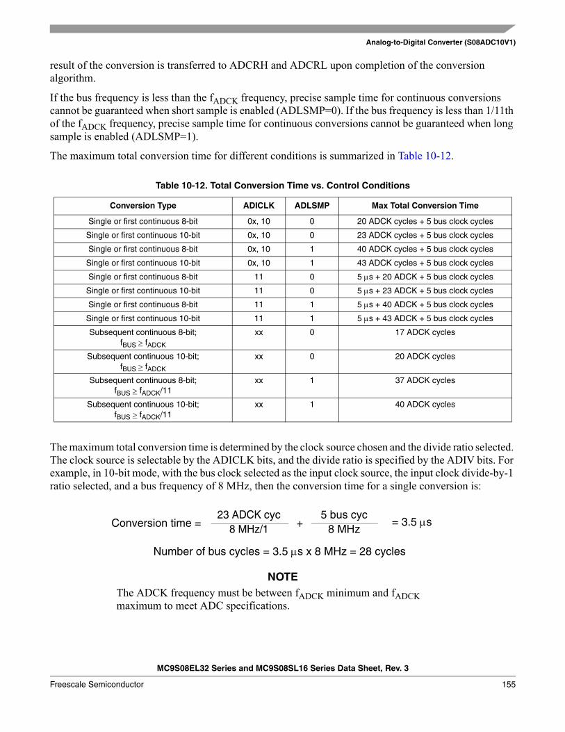
Analog-to-Digital Converter (S08ADC10V1)
MC9S08EL32 Series and MC9S08SL16 Series Data Sheet, Rev. 3
Freescale Semiconductor 155
result of the conversion is transferred to ADCRH and ADCRL upon completion of the conversion algorithm.
If the bus frequency is less than the fADCK frequency, precise sample time for continuous conversions cannot be guaranteed when short sample is enabled (ADLSMP=0). If the bus frequency is less than 1/11th of the fADCK frequency, precise sample time for continuous conversions cannot be guaranteed when long sample is enabled (ADLSMP=1).
The maximum total conversion time for different conditions is summarized in Table 10-12.
The maximum total conversion time is determined by the clock source chosen and the divide ratio selected. The clock source is selectable by the ADICLK bits, and the divide ratio is specified by the ADIV bits. For example, in 10-bit mode, with the bus clock selected as the input clock source, the input clock divide-by-1 ratio selected, and a bus frequency of 8 MHz, then the conversion time for a single conversion is:
NOTEThe ADCK frequency must be between fADCK minimum and fADCK maximum to meet ADC specifications.
Table 10-12. Total Conversion Time vs. Control Conditions
Conversion Type ADICLK ADLSMP Max Total Conversion Time
Single or first continuous 8-bit 0x, 10 0 20 ADCK cycles + 5 bus clock cycles
Single or first continuous 10-bit 0x, 10 0 23 ADCK cycles + 5 bus clock cycles
Single or first continuous 8-bit 0x, 10 1 40 ADCK cycles + 5 bus clock cycles
Single or first continuous 10-bit 0x, 10 1 43 ADCK cycles + 5 bus clock cycles
Single or first continuous 8-bit 11 0 5 μs + 20 ADCK + 5 bus clock cycles
Single or first continuous 10-bit 11 0 5 μs + 23 ADCK + 5 bus clock cycles
Single or first continuous 8-bit 11 1 5 μs + 40 ADCK + 5 bus clock cycles
Single or first continuous 10-bit 11 1 5 μs + 43 ADCK + 5 bus clock cycles
Subsequent continuous 8-bit; fBUS > fADCK
xx 0 17 ADCK cycles
Subsequent continuous 10-bit; fBUS > fADCK
xx 0 20 ADCK cycles
Subsequent continuous 8-bit; fBUS > fADCK/11
xx 1 37 ADCK cycles
Subsequent continuous 10-bit; fBUS > fADCK/11
xx 1 40 ADCK cycles
23 ADCK cycConversion time = 8 MHz/1
Number of bus cycles = 3.5 μs x 8 MHz = 28 cycles
5 bus cyc8 MHz+ = 3.5 μs
Analog-to-Digital Converter (S08ADC10V1)
MC9S08EL32 Series and MC9S08SL16 Series Data Sheet, Rev. 3
156 Freescale Semiconductor
10.4.5 Automatic Compare Function
The compare function can be configured to check for either an upper limit or lower limit. After the input is sampled and converted, the result is added to the two’s complement of the compare value (ADCCVH and ADCCVL). When comparing to an upper limit (ACFGT = 1), if the result is greater-than or equal-to the compare value, COCO is set. When comparing to a lower limit (ACFGT = 0), if the result is less than the compare value, COCO is set. The value generated by the addition of the conversion result and the two’s complement of the compare value is transferred to ADCRH and ADCRL.
Upon completion of a conversion while the compare function is enabled, if the compare condition is not true, COCO is not set and no data is transferred to the result registers. An ADC interrupt is generated upon the setting of COCO if the ADC interrupt is enabled (AIEN = 1).
NOTEThe compare function can be used to monitor the voltage on a channel while the MCU is in either wait or stop3 mode. The ADC interrupt will wake the MCU when the compare condition is met.
10.4.6 MCU Wait Mode Operation
The WAIT instruction puts the MCU in a lower power-consumption standby mode from which recovery is very fast because the clock sources remain active. If a conversion is in progress when the MCU enters wait mode, it continues until completion. Conversions can be initiated while the MCU is in wait mode by means of the hardware trigger or if continuous conversions are enabled.
The bus clock, bus clock divided by two, and ADACK are available as conversion clock sources while in wait mode. The use of ALTCLK as the conversion clock source in wait is dependent on the definition of ALTCLK for this MCU. Consult the module introduction for information on ALTCLK specific to this MCU.
A conversion complete event sets the COCO and generates an ADC interrupt to wake the MCU from wait mode if the ADC interrupt is enabled (AIEN = 1).
10.4.7 MCU Stop3 Mode Operation
The STOP instruction is used to put the MCU in a low power-consumption standby mode during which most or all clock sources on the MCU are disabled.
10.4.7.1 Stop3 Mode With ADACK Disabled
If the asynchronous clock, ADACK, is not selected as the conversion clock, executing a STOP instruction aborts the current conversion and places the ADC in its idle state. The contents of ADCRH and ADCRL are unaffected by stop3 mode.After exiting from stop3 mode, a software or hardware trigger is required to resume conversions.
Analog-to-Digital Converter (S08ADC10V1)
MC9S08EL32 Series and MC9S08SL16 Series Data Sheet, Rev. 3
Freescale Semiconductor 157
10.4.7.2 Stop3 Mode With ADACK Enabled
If ADACK is selected as the conversion clock, the ADC continues operation during stop3 mode. For guaranteed ADC operation, the MCU’s voltage regulator must remain active during stop3 mode. Consult the module introduction for configuration information for this MCU.
If a conversion is in progress when the MCU enters stop3 mode, it continues until completion. Conversions can be initiated while the MCU is in stop3 mode by means of the hardware trigger or if continuous conversions are enabled.
A conversion complete event sets the COCO and generates an ADC interrupt to wake the MCU from stop3 mode if the ADC interrupt is enabled (AIEN = 1).
NOTEIt is possible for the ADC module to wake the system from low power stop and cause the MCU to begin consuming run-level currents without generating a system level interrupt. To prevent this scenario, software should ensure that the data transfer blocking mechanism (discussed in Section 10.4.4.2, “Completing Conversions) is cleared when entering stop3 and continuing ADC conversions.
10.4.8 MCU Stop1 and Stop2 Mode Operation
The ADC module is automatically disabled when the MCU enters either stop1 or stop2 mode. All module registers contain their reset values following exit from stop1 or stop2. Therefore the module must be re-enabled and re-configured following exit from stop1 or stop2.
10.5 Initialization InformationThis section gives an example which provides some basic direction on how a user would initialize and configure the ADC module. The user has the flexibility of choosing between configuring the module for 8-bit or 10-bit resolution, single or continuous conversion, and a polled or interrupt approach, among many other options. Refer to Table 10-6, Table 10-7, and Table 10-8 for information used in this example.
NOTEHexadecimal values designated by a preceding 0x, binary values designated by a preceding %, and decimal values have no preceding character.
10.5.1 ADC Module Initialization Example
10.5.1.1 Initialization Sequence
Before the ADC module can be used to complete conversions, an initialization procedure must be performed. A typical sequence is as follows:
1. Update the configuration register (ADCCFG) to select the input clock source and the divide ratio used to generate the internal clock, ADCK. This register is also used for selecting sample time and low-power configuration.
Analog-to-Digital Converter (S08ADC10V1)
MC9S08EL32 Series and MC9S08SL16 Series Data Sheet, Rev. 3
158 Freescale Semiconductor
2. Update status and control register 2 (ADCSC2) to select the conversion trigger (hardware or software) and compare function options, if enabled.
3. Update status and control register 1 (ADCSC1) to select whether conversions will be continuous or completed only once, and to enable or disable conversion complete interrupts. The input channel on which conversions will be performed is also selected here.
10.5.1.2 Pseudo — Code Example
In this example, the ADC module will be set up with interrupts enabled to perform a single 10-bit conversion at low power with a long sample time on input channel 1, where the internal ADCK clock will be derived from the bus clock divided by 1.
ADCCFG = 0x98 (%10011000) Bit 7 ADLPC 1 Configures for low power (lowers maximum clock speed)Bit 6:5 ADIV 00 Sets the ADCK to the input clock ÷ 1Bit 4 ADLSMP 1 Configures for long sample timeBit 3:2 MODE 10 Sets mode at 10-bit conversionsBit 1:0 ADICLK 00 Selects bus clock as input clock source
ADCSC2 = 0x00 (%00000000)Bit 7 ADACT 0 Flag indicates if a conversion is in progressBit 6 ADTRG 0 Software trigger selectedBit 5 ACFE 0 Compare function disabledBit 4 ACFGT 0 Not used in this exampleBit 3:2 00 Unimplemented or reserved, always reads zeroBit 1:0 00 Reserved for Freescale’s internal use; always write zero
ADCSC1 = 0x41 (%01000001)Bit 7 COCO 0 Read-only flag which is set when a conversion completesBit 6 AIEN 1 Conversion complete interrupt enabledBit 5 ADCO 0 One conversion only (continuous conversions disabled)Bit 4:0 ADCH 00001 Input channel 1 selected as ADC input channel
ADCRH/L = 0xxxHolds results of conversion. Read high byte (ADCRH) before low byte (ADCRL) so that conversion
data cannot be overwritten with data from the next conversion.
ADCCVH/L = 0xxxHolds compare value when compare function enabled
APCTL1=0x02 AD1 pin I/O control disabled. All other AD pins remain general purpose I/O pins
APCTL2=0x00All other AD pins remain general purpose I/O pins
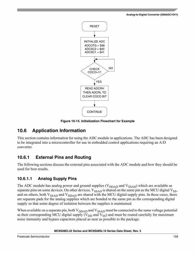
Analog-to-Digital Converter (S08ADC10V1)
MC9S08EL32 Series and MC9S08SL16 Series Data Sheet, Rev. 3
Freescale Semiconductor 159
Figure 10-14. Initialization Flowchart for Example
10.6 Application InformationThis section contains information for using the ADC module in applications. The ADC has been designed to be integrated into a microcontroller for use in embedded control applications requiring an A/D converter.
10.6.1 External Pins and Routing
The following sections discuss the external pins associated with the ADC module and how they should be used for best results.
10.6.1.1 Analog Supply Pins
The ADC module has analog power and ground supplies (VDDAD and VSSAD) which are available as separate pins on some devices. On other devices, VSSAD is shared on the same pin as the MCU digital VSS, and on others, both VSSAD and VDDAD are shared with the MCU digital supply pins. In these cases, there are separate pads for the analog supplies which are bonded to the same pin as the corresponding digital supply so that some degree of isolation between the supplies is maintained.
When available on a separate pin, both VDDAD and VSSAD must be connected to the same voltage potential as their corresponding MCU digital supply (VDD and VSS) and must be routed carefully for maximum noise immunity and bypass capacitors placed as near as possible to the package.
YES
NO
RESET
INITIALIZE ADCADCCFG = $98
ADCSC1 = $41ADCSC2 = $00
CHECKCOCO=1?
READ ADCRHTHEN ADCRL TOCLEAR COCO BIT
CONTINUE
Analog-to-Digital Converter (S08ADC10V1)
MC9S08EL32 Series and MC9S08SL16 Series Data Sheet, Rev. 3
160 Freescale Semiconductor
In cases where separate power supplies are used for analog and digital power, the ground connection between these supplies must be at the VSSAD pin. This should be the only ground connection between these supplies if possible. The VSSAD pin makes a good single point ground location.
10.6.1.2 Analog Reference Pins
In addition to the analog supplies, the ADC module has connections for two reference voltage inputs. The high reference is VREFH, which may be shared on the same pin as VDDAD on some devices. The low reference is VREFL, which may be shared on the same pin as VSSAD on some devices.
When available on a separate pin, VREFH may be connected to the same potential as VDDAD, or may be driven by an external source that is between the minimum VDDAD spec and the VDDAD potential (VREFH must never exceed VDDAD). When available on a separate pin, VREFL must be connected to the same voltage potential as VSSAD. Both VREFH and VREFL must be routed carefully for maximum noise immunity and bypass capacitors placed as near as possible to the package.
AC current in the form of current spikes required to supply charge to the capacitor array at each successive approximation step is drawn through the VREFH and VREFL loop. The best external component to meet this current demand is a 0.1 μF capacitor with good high frequency characteristics. This capacitor is connected between VREFH and VREFL and must be placed as near as possible to the package pins. Resistance in the path is not recommended because the current will cause a voltage drop which could result in conversion errors. Inductance in this path must be minimum (parasitic only).
10.6.1.3 Analog Input Pins
The external analog inputs are typically shared with digital I/O pins on MCU devices. The pin I/O control is disabled by setting the appropriate control bit in one of the pin control registers. Conversions can be performed on inputs without the associated pin control register bit set. It is recommended that the pin control register bit always be set when using a pin as an analog input. This avoids problems with contention because the output buffer will be in its high impedance state and the pullup is disabled. Also, the input buffer draws dc current when its input is not at either VDD or VSS. Setting the pin control register bits for all pins used as analog inputs should be done to achieve lowest operating current.
Empirical data shows that capacitors on the analog inputs improve performance in the presence of noise or when the source impedance is high. Use of 0.01 μF capacitors with good high-frequency characteristics is sufficient. These capacitors are not necessary in all cases, but when used they must be placed as near as possible to the package pins and be referenced to VSSA.
For proper conversion, the input voltage must fall between VREFH and VREFL. If the input is equal to or exceeds VREFH, the converter circuit converts the signal to $3FF (full scale 10-bit representation) or $FF (full scale 8-bit representation). If the input is equal to or less than VREFL, the converter circuit converts it to $000. Input voltages between VREFH and VREFL are straight-line linear conversions. There will be a brief current associated with VREFL when the sampling capacitor is charging. The input is sampled for 3.5 cycles of the ADCK source when ADLSMP is low, or 23.5 cycles when ADLSMP is high.
For minimal loss of accuracy due to current injection, pins adjacent to the analog input pins should not be transitioning during conversions.
Analog-to-Digital Converter (S08ADC10V1)
MC9S08EL32 Series and MC9S08SL16 Series Data Sheet, Rev. 3
Freescale Semiconductor 161
10.6.2 Sources of Error
Several sources of error exist for A/D conversions. These are discussed in the following sections.
10.6.2.1 Sampling Error
For proper conversions, the input must be sampled long enough to achieve the proper accuracy. Given the maximum input resistance of approximately 7kΩ and input capacitance of approximately 5.5 pF, sampling to within 1/4LSB (at 10-bit resolution) can be achieved within the minimum sample window (3.5 cycles @ 8 MHz maximum ADCK frequency) provided the resistance of the external analog source (RAS) is kept below 5 kΩ.
Higher source resistances or higher-accuracy sampling is possible by setting ADLSMP (to increase the sample window to 23.5 cycles) or decreasing ADCK frequency to increase sample time.
10.6.2.2 Pin Leakage Error
Leakage on the I/O pins can cause conversion error if the external analog source resistance (RAS) is high. If this error cannot be tolerated by the application, keep RAS lower than VDDAD / (2N*ILEAK) for less than 1/4LSB leakage error (N = 8 in 8-bit mode or 10 in 10-bit mode).
10.6.2.3 Noise-Induced Errors
System noise which occurs during the sample or conversion process can affect the accuracy of the conversion. The ADC accuracy numbers are guaranteed as specified only if the following conditions are met:
• There is a 0.1 μF low-ESR capacitor from VREFH to VREFL.• There is a 0.1 μF low-ESR capacitor from VDDAD to VSSAD.• If inductive isolation is used from the primary supply, an additional 1 μF capacitor is placed from
VDDAD to VSSAD.• VSSAD (and VREFL, if connected) is connected to VSS at a quiet point in the ground plane.• Operate the MCU in wait or stop3 mode before initiating (hardware triggered conversions) or
immediately after initiating (hardware or software triggered conversions) the ADC conversion. — For software triggered conversions, immediately follow the write to the ADCSC1 with a WAIT
instruction or STOP instruction.— For stop3 mode operation, select ADACK as the clock source. Operation in stop3 reduces VDD
noise but increases effective conversion time due to stop recovery.• There is no I/O switching, input or output, on the MCU during the conversion.
There are some situations where external system activity causes radiated or conducted noise emissions or excessive VDD noise is coupled into the ADC. In these situations, or when the MCU cannot be placed in wait or stop3 or I/O activity cannot be halted, these recommended actions may reduce the effect of noise on the accuracy:
• Place a 0.01 μF capacitor (CAS) on the selected input channel to VREFL or VSSAD (this will improve noise issues but will affect sample rate based on the external analog source resistance).
Analog-to-Digital Converter (S08ADC10V1)
MC9S08EL32 Series and MC9S08SL16 Series Data Sheet, Rev. 3
162 Freescale Semiconductor
• Average the result by converting the analog input many times in succession and dividing the sum of the results. Four samples are required to eliminate the effect of a 1LSB, one-time error.
• Reduce the effect of synchronous noise by operating off the asynchronous clock (ADACK) and averaging. Noise that is synchronous to ADCK cannot be averaged out.
10.6.2.4 Code Width and Quantization Error
The ADC quantizes the ideal straight-line transfer function into 1024 steps (in 10-bit mode). Each step ideally has the same height (1 code) and width. The width is defined as the delta between the transition points to one code and the next. The ideal code width for an N bit converter (in this case N can be 8 or 10), defined as 1LSB, is:
1LSB = (VREFH - VREFL) / 2N Eqn. 10-2
There is an inherent quantization error due to the digitization of the result. For 8-bit or 10-bit conversions the code will transition when the voltage is at the midpoint between the points where the straight line transfer function is exactly represented by the actual transfer function. Therefore, the quantization error will be ± 1/2LSB in 8- or 10-bit mode. As a consequence, however, the code width of the first ($000) conversion is only 1/2LSB and the code width of the last ($FF or $3FF) is 1.5LSB.
10.6.2.5 Linearity Errors
The ADC may also exhibit non-linearity of several forms. Every effort has been made to reduce these errors but the system should be aware of them because they affect overall accuracy. These errors are:
• Zero-scale error (EZS) (sometimes called offset) — This error is defined as the difference between the actual code width of the first conversion and the ideal code width (1/2LSB). Note, if the first conversion is $001, then the difference between the actual $001 code width and its ideal (1LSB) is used.
• Full-scale error (EFS) — This error is defined as the difference between the actual code width of the last conversion and the ideal code width (1.5LSB). Note, if the last conversion is $3FE, then the difference between the actual $3FE code width and its ideal (1LSB) is used.
• Differential non-linearity (DNL) — This error is defined as the worst-case difference between the actual code width and the ideal code width for all conversions.
• Integral non-linearity (INL) — This error is defined as the highest-value the (absolute value of the) running sum of DNL achieves. More simply, this is the worst-case difference of the actual transition voltage to a given code and its corresponding ideal transition voltage, for all codes.
• Total unadjusted error (TUE) — This error is defined as the difference between the actual transfer function and the ideal straight-line transfer function, and therefore includes all forms of error.
10.6.2.6 Code Jitter, Non-Monotonicity and Missing Codes
Analog-to-digital converters are susceptible to three special forms of error. These are code jitter, non-monotonicity, and missing codes.
Code jitter is when, at certain points, a given input voltage converts to one of two values when sampled repeatedly. Ideally, when the input voltage is infinitesimally smaller than the transition voltage, the

Analog-to-Digital Converter (S08ADC10V1)
MC9S08EL32 Series and MC9S08SL16 Series Data Sheet, Rev. 3
Freescale Semiconductor 163
converter yields the lower code (and vice-versa). However, even very small amounts of system noise can cause the converter to be indeterminate (between two codes) for a range of input voltages around the transition voltage. This range is normally around ±1/2 LSB and will increase with noise. This error may be reduced by repeatedly sampling the input and averaging the result. Additionally the techniques discussed in Section 10.6.2.3 will reduce this error.
Non-monotonicity is defined as when, except for code jitter, the converter converts to a lower code for a higher input voltage. Missing codes are those values which are never converted for any input value.
In 8-bit or 10-bit mode, the ADC is guaranteed to be monotonic and to have no missing codes.

Analog-to-Digital Converter (S08ADC10V1)
MC9S08EL32 Series and MC9S08SL16 Series Data Sheet, Rev. 3
164 Freescale Semiconductor
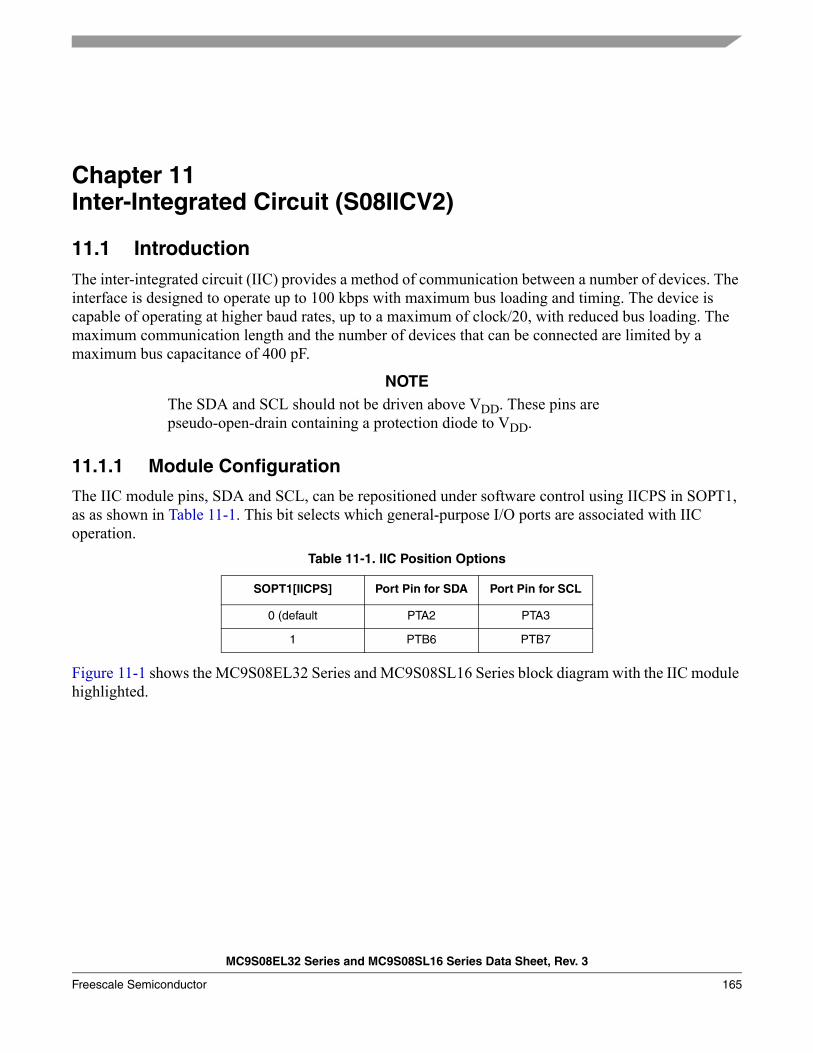
MC9S08EL32 Series and MC9S08SL16 Series Data Sheet, Rev. 3
Freescale Semiconductor 165
Chapter 11 Inter-Integrated Circuit (S08IICV2)
11.1 IntroductionThe inter-integrated circuit (IIC) provides a method of communication between a number of devices. The interface is designed to operate up to 100 kbps with maximum bus loading and timing. The device is capable of operating at higher baud rates, up to a maximum of clock/20, with reduced bus loading. The maximum communication length and the number of devices that can be connected are limited by a maximum bus capacitance of 400 pF.
NOTEThe SDA and SCL should not be driven above VDD. These pins are pseudo-open-drain containing a protection diode to VDD.
11.1.1 Module Configuration
The IIC module pins, SDA and SCL, can be repositioned under software control using IICPS in SOPT1, as as shown in Table 11-1. This bit selects which general-purpose I/O ports are associated with IIC operation.
Figure 11-1 shows the MC9S08EL32 Series and MC9S08SL16 Series block diagram with the IIC module highlighted.
Table 11-1. IIC Position Options
SOPT1[IICPS] Port Pin for SDA Port Pin for SCL
0 (default PTA2 PTA3
1 PTB6 PTB7
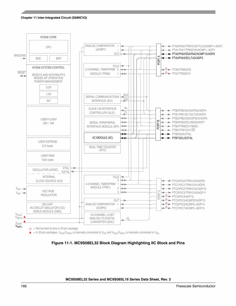
Chapter 11 Inter-Integrated Circuit (S08IICV2)
MC9S08EL32 Series and MC9S08SL16 Series Data Sheet, Rev. 3
166 Freescale Semiconductor
Figure 11-1. MC9S08EL32 Block Diagram Highlighting IIC Block and Pins
VSS
IIC MODULE (IIC)
SERIAL PERIPHERAL INTERFACE MODULE (SPI)
USER FLASH
USER RAM
32K / 16K
HCS08 CORE
CPU
BDC
2-CHANNEL TIMER/PWMMODULE (TPM2)
HCS08 SYSTEM CONTROL
RESETS AND INTERRUPTSMODES OF OPERATIONPOWER MANAGEMENT
VOLTAGE REGULATOR
COP
LVD
OSCILLATOR (XOSC)
INTERNALCLOCK SOURCE (ICS)
RESET
VREFH
1024 bytes
INTERFACE (SCI)SERIAL COMMUNICATIONS
XTALEXTAL
4-CHANNEL TIMER/PWMMODULE (TPM1)
REAL-TIME COUNTER
IN-CIRCUIT EMULATOR (ICE)
BKGD/MS PTA3/PIA3/SCL/TxD/ADP3
PTA6/TPM2CH0
PTA2/PIA2/SDA/RxD/ACMP1O/ADP2PTA1/PIA1/TPM2CH0/ACMP1–/ADP1PTA0/PIA0/TPM1CH0/TCLK/ACMP1+/ADP0
PTA7/TPM2CH1
PTB3/PIB3/SCL/MOSI/ADP7PTB4/TPM2CH1/MISO
PTB2/PIB2/SDA/SPSCK/ADP6PTB1/PIB1/SLTxD/TxD/ADP5PTB0/PIB0/SLRxD/RxD/ADP4
PTB7/SCL/EXTAL
PTC3/PIC3/TPM1CH3/ADP11PTC4/PIC4/ADP12PTC5/PIC5/ACMP2O/ADP13
PTC2/PIC2/TPM1CH2/ADP10PTC1/PIC1/TPM1CH1/ADP9
POR
T C
PTC6/PIC6/ACMP2+/ADP14
VDD
BKP
INT
ANALOG COMPARATOR(ACMP2)
USER EEPROM512 bytes
CONTROLLER (SLIC)SLAVE LIN INTERFACE
ANALOG-TO-DIGITALCONVERTER (ADC)
16-CHANNEL,10-BIT16
= In 20-pin packages, VDDA/VREFH is internally connected to VDD and VSSA/VREFL is internally connected to VSS.
VDDA/
VREFL
VSSA/
DEBUG MODULE (DBG)
ON-CHIP
(RTC)
PTC0/PIC0/TPM1CH0/ADP8
PTC7/PIC7/ACMP2–/ADP15
PTB6/SDA/XTAL
POR
T B
POR
T A
PTB5/TPM1CH1/SS
ANALOG COMPARATOR(ACMP1)
= Not bonded to pins in 20-pin package
TCLK
TCLK
+–
OUT
+–
OUT
0123
10
RxDTxD
TxRx
Inter-Integrated Circuit (S08IICV2)
MC9S08EL32 Series and MC9S08SL16 Series Data Sheet, Rev. 3Freescale Semiconductor 167
11.1.2 Features
The IIC includes these distinctive features:• Compatible with IIC bus standard• Multi-master operation• Software programmable for one of 64 different serial clock frequencies• Software selectable acknowledge bit• Interrupt driven byte-by-byte data transfer• Arbitration lost interrupt with automatic mode switching from master to slave• Calling address identification interrupt• Start and stop signal generation/detection• Repeated start signal generation• Acknowledge bit generation/detection• Bus busy detection• General call recognition• 10-bit address extension
11.1.3 Modes of Operation
A brief description of the IIC in the various MCU modes is given here. • Run mode — This is the basic mode of operation. To conserve power in this mode, disable the
module.• Wait mode — The module continues to operate while the MCU is in wait mode and can provide
a wake-up interrupt.• Stop mode — The IIC is inactive in stop3 mode for reduced power consumption. The stop
instruction does not affect IIC register states. Stop2 resets the register contents.
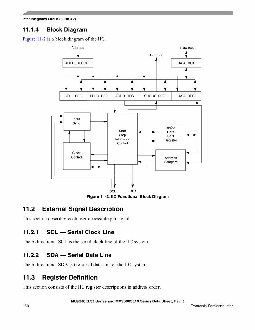
Inter-Integrated Circuit (S08IICV2)
MC9S08EL32 Series and MC9S08SL16 Series Data Sheet, Rev. 3168 Freescale Semiconductor
11.1.4 Block Diagram
Figure 11-2 is a block diagram of the IIC.
Figure 11-2. IIC Functional Block Diagram
11.2 External Signal DescriptionThis section describes each user-accessible pin signal.
11.2.1 SCL — Serial Clock Line
The bidirectional SCL is the serial clock line of the IIC system.
11.2.2 SDA — Serial Data Line
The bidirectional SDA is the serial data line of the IIC system.
11.3 Register DefinitionThis section consists of the IIC register descriptions in address order.
InputSync
In/OutDataShift
Register
AddressCompare
Interrupt
ClockControl
StartStop
ArbitrationControl
CTRL_REG FREQ_REG ADDR_REG STATUS_REG DATA_REG
ADDR_DECODE DATA_MUX
Data Bus
SCL SDA
Address
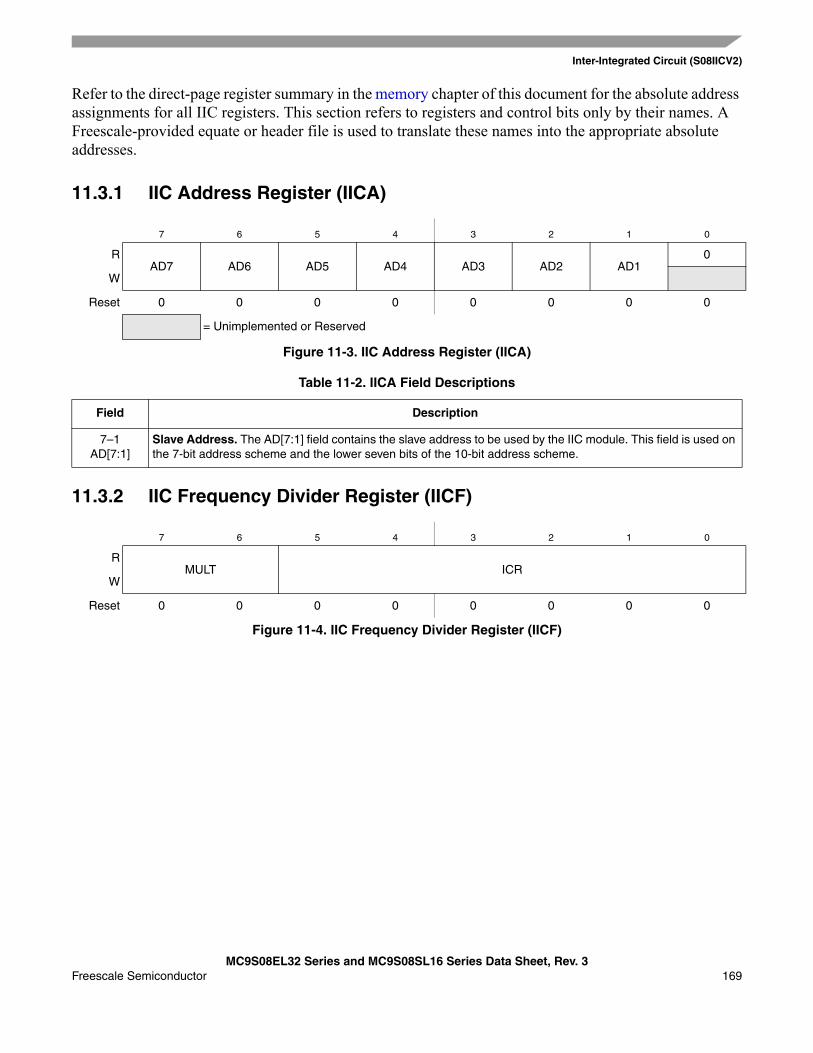
Inter-Integrated Circuit (S08IICV2)
MC9S08EL32 Series and MC9S08SL16 Series Data Sheet, Rev. 3Freescale Semiconductor 169
Refer to the direct-page register summary in the memory chapter of this document for the absolute address assignments for all IIC registers. This section refers to registers and control bits only by their names. A Freescale-provided equate or header file is used to translate these names into the appropriate absolute addresses.
11.3.1 IIC Address Register (IICA)
11.3.2 IIC Frequency Divider Register (IICF)
7 6 5 4 3 2 1 0
RAD7 AD6 AD5 AD4 AD3 AD2 AD1
0
W
Reset 0 0 0 0 0 0 0 0
= Unimplemented or Reserved
Figure 11-3. IIC Address Register (IICA)
Table 11-2. IICA Field Descriptions
Field Description
7–1AD[7:1]
Slave Address. The AD[7:1] field contains the slave address to be used by the IIC module. This field is used on the 7-bit address scheme and the lower seven bits of the 10-bit address scheme.
7 6 5 4 3 2 1 0
RMULT ICR
W
Reset 0 0 0 0 0 0 0 0
Figure 11-4. IIC Frequency Divider Register (IICF)
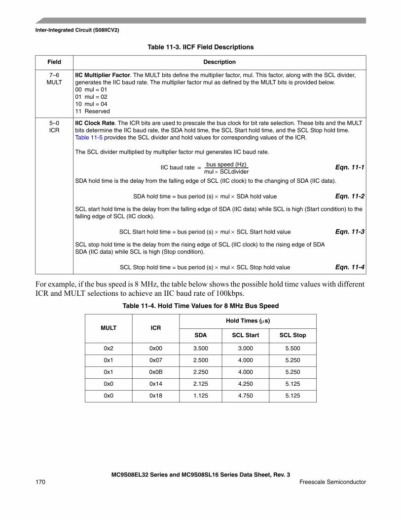
Inter-Integrated Circuit (S08IICV2)
MC9S08EL32 Series and MC9S08SL16 Series Data Sheet, Rev. 3170 Freescale Semiconductor
For example, if the bus speed is 8 MHz, the table below shows the possible hold time values with different ICR and MULT selections to achieve an IIC baud rate of 100kbps.
Table 11-3. IICF Field Descriptions
Field Description
7–6MULT
IIC Multiplier Factor. The MULT bits define the multiplier factor, mul. This factor, along with the SCL divider, generates the IIC baud rate. The multiplier factor mul as defined by the MULT bits is provided below.00 mul = 0101 mul = 0210 mul = 0411 Reserved
5–0ICR
IIC Clock Rate. The ICR bits are used to prescale the bus clock for bit rate selection. These bits and the MULT bits determine the IIC baud rate, the SDA hold time, the SCL Start hold time, and the SCL Stop hold time. Table 11-5 provides the SCL divider and hold values for corresponding values of the ICR.
The SCL divider multiplied by multiplier factor mul generates IIC baud rate.
Eqn. 11-1
SDA hold time is the delay from the falling edge of SCL (IIC clock) to the changing of SDA (IIC data).
SDA hold time = bus period (s) × mul × SDA hold value Eqn. 11-2
SCL start hold time is the delay from the falling edge of SDA (IIC data) while SCL is high (Start condition) to the falling edge of SCL (IIC clock).
SCL Start hold time = bus period (s) × mul × SCL Start hold value Eqn. 11-3
SCL stop hold time is the delay from the rising edge of SCL (IIC clock) to the rising edge of SDASDA (IIC data) while SCL is high (Stop condition).
SCL Stop hold time = bus period (s) × mul × SCL Stop hold value Eqn. 11-4
Table 11-4. Hold Time Values for 8 MHz Bus Speed
MULT ICRHold Times (μs)
SDA SCL Start SCL Stop
0x2 0x00 3.500 3.000 5.500
0x1 0x07 2.500 4.000 5.250
0x1 0x0B 2.250 4.000 5.250
0x0 0x14 2.125 4.250 5.125
0x0 0x18 1.125 4.750 5.125
IIC baud rate bus speed (Hz)mul SCLdivider×---------------------------------------------=
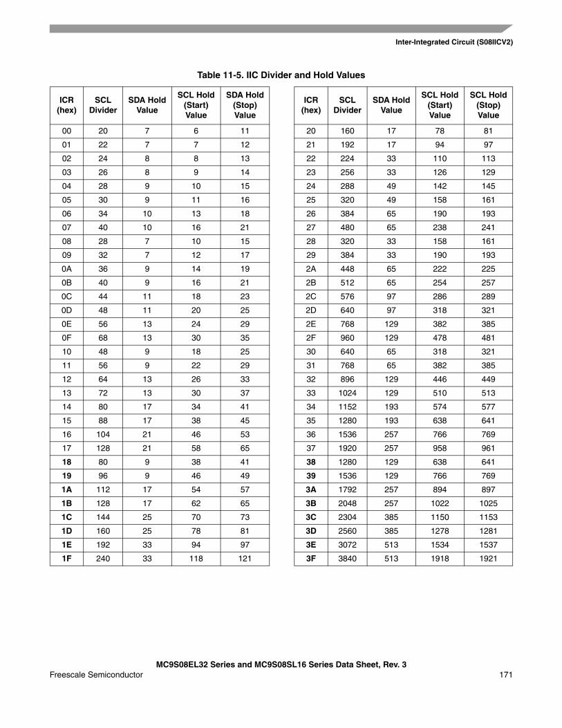
Inter-Integrated Circuit (S08IICV2)
MC9S08EL32 Series and MC9S08SL16 Series Data Sheet, Rev. 3Freescale Semiconductor 171
Table 11-5. IIC Divider and Hold Values
ICR(hex)
SCL Divider
SDA HoldValue
SCL Hold(Start) Value
SDA Hold(Stop) Value
ICR(hex)
SCL Divider
SDA HoldValue
SCL Hold(Start) Value
SCL Hold(Stop) Value
00 20 7 6 11 20 160 17 78 81
01 22 7 7 12 21 192 17 94 97
02 24 8 8 13 22 224 33 110 113
03 26 8 9 14 23 256 33 126 129
04 28 9 10 15 24 288 49 142 145
05 30 9 11 16 25 320 49 158 161
06 34 10 13 18 26 384 65 190 193
07 40 10 16 21 27 480 65 238 241
08 28 7 10 15 28 320 33 158 161
09 32 7 12 17 29 384 33 190 193
0A 36 9 14 19 2A 448 65 222 225
0B 40 9 16 21 2B 512 65 254 257
0C 44 11 18 23 2C 576 97 286 289
0D 48 11 20 25 2D 640 97 318 321
0E 56 13 24 29 2E 768 129 382 385
0F 68 13 30 35 2F 960 129 478 481
10 48 9 18 25 30 640 65 318 321
11 56 9 22 29 31 768 65 382 385
12 64 13 26 33 32 896 129 446 449
13 72 13 30 37 33 1024 129 510 513
14 80 17 34 41 34 1152 193 574 577
15 88 17 38 45 35 1280 193 638 641
16 104 21 46 53 36 1536 257 766 769
17 128 21 58 65 37 1920 257 958 961
18 80 9 38 41 38 1280 129 638 641
19 96 9 46 49 39 1536 129 766 769
1A 112 17 54 57 3A 1792 257 894 897
1B 128 17 62 65 3B 2048 257 1022 1025
1C 144 25 70 73 3C 2304 385 1150 1153
1D 160 25 78 81 3D 2560 385 1278 1281
1E 192 33 94 97 3E 3072 513 1534 1537
1F 240 33 118 121 3F 3840 513 1918 1921
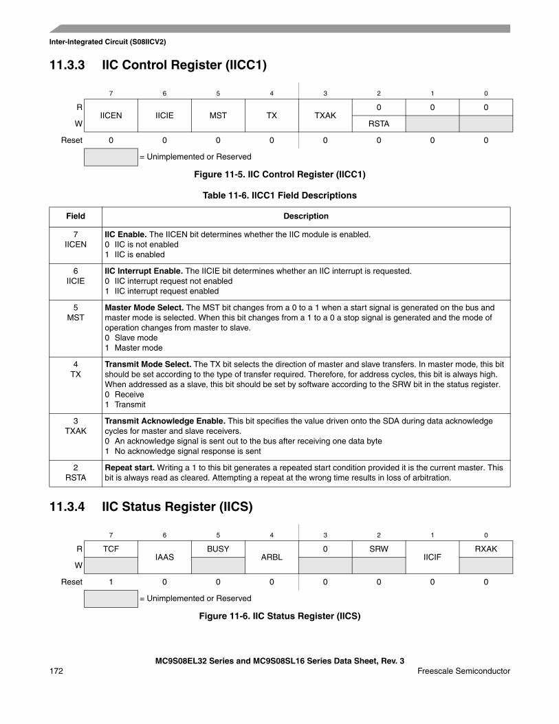
Inter-Integrated Circuit (S08IICV2)
MC9S08EL32 Series and MC9S08SL16 Series Data Sheet, Rev. 3172 Freescale Semiconductor
11.3.3 IIC Control Register (IICC1)
11.3.4 IIC Status Register (IICS)
7 6 5 4 3 2 1 0
RIICEN IICIE MST TX TXAK
0 0 0
W RSTA
Reset 0 0 0 0 0 0 0 0
= Unimplemented or Reserved
Figure 11-5. IIC Control Register (IICC1)
Table 11-6. IICC1 Field Descriptions
Field Description
7IICEN
IIC Enable. The IICEN bit determines whether the IIC module is enabled.0 IIC is not enabled1 IIC is enabled
6IICIE
IIC Interrupt Enable. The IICIE bit determines whether an IIC interrupt is requested.0 IIC interrupt request not enabled1 IIC interrupt request enabled
5MST
Master Mode Select. The MST bit changes from a 0 to a 1 when a start signal is generated on the bus and master mode is selected. When this bit changes from a 1 to a 0 a stop signal is generated and the mode of operation changes from master to slave.0 Slave mode1 Master mode
4TX
Transmit Mode Select. The TX bit selects the direction of master and slave transfers. In master mode, this bit should be set according to the type of transfer required. Therefore, for address cycles, this bit is always high. When addressed as a slave, this bit should be set by software according to the SRW bit in the status register.0 Receive1 Transmit
3TXAK
Transmit Acknowledge Enable. This bit specifies the value driven onto the SDA during data acknowledge cycles for master and slave receivers.0 An acknowledge signal is sent out to the bus after receiving one data byte1 No acknowledge signal response is sent
2RSTA
Repeat start. Writing a 1 to this bit generates a repeated start condition provided it is the current master. This bit is always read as cleared. Attempting a repeat at the wrong time results in loss of arbitration.
7 6 5 4 3 2 1 0
R TCFIAAS
BUSYARBL
0 SRWIICIF
RXAK
W
Reset 1 0 0 0 0 0 0 0
= Unimplemented or Reserved
Figure 11-6. IIC Status Register (IICS)
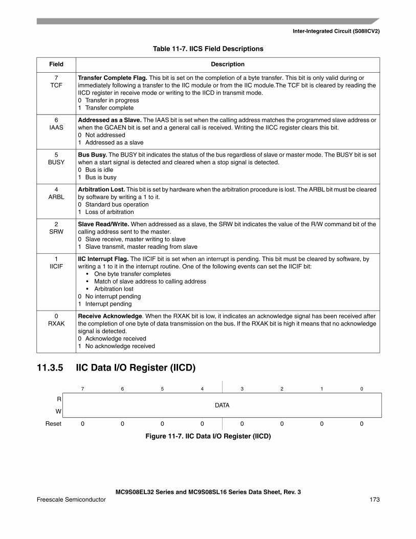
Inter-Integrated Circuit (S08IICV2)
MC9S08EL32 Series and MC9S08SL16 Series Data Sheet, Rev. 3Freescale Semiconductor 173
11.3.5 IIC Data I/O Register (IICD)
Table 11-7. IICS Field Descriptions
Field Description
7TCF
Transfer Complete Flag. This bit is set on the completion of a byte transfer. This bit is only valid during or immediately following a transfer to the IIC module or from the IIC module.The TCF bit is cleared by reading the IICD register in receive mode or writing to the IICD in transmit mode.0 Transfer in progress1 Transfer complete
6IAAS
Addressed as a Slave. The IAAS bit is set when the calling address matches the programmed slave address or when the GCAEN bit is set and a general call is received. Writing the IICC register clears this bit.0 Not addressed1 Addressed as a slave
5BUSY
Bus Busy. The BUSY bit indicates the status of the bus regardless of slave or master mode. The BUSY bit is set when a start signal is detected and cleared when a stop signal is detected.0 Bus is idle1 Bus is busy
4ARBL
Arbitration Lost. This bit is set by hardware when the arbitration procedure is lost. The ARBL bit must be cleared by software by writing a 1 to it. 0 Standard bus operation1 Loss of arbitration
2SRW
Slave Read/Write. When addressed as a slave, the SRW bit indicates the value of the R/W command bit of the calling address sent to the master. 0 Slave receive, master writing to slave1 Slave transmit, master reading from slave
1IICIF
IIC Interrupt Flag. The IICIF bit is set when an interrupt is pending. This bit must be cleared by software, by writing a 1 to it in the interrupt routine. One of the following events can set the IICIF bit:
• One byte transfer completes• Match of slave address to calling address• Arbitration lost
0 No interrupt pending1 Interrupt pending
0RXAK
Receive Acknowledge. When the RXAK bit is low, it indicates an acknowledge signal has been received after the completion of one byte of data transmission on the bus. If the RXAK bit is high it means that no acknowledge signal is detected.0 Acknowledge received1 No acknowledge received
7 6 5 4 3 2 1 0
RDATA
W
Reset 0 0 0 0 0 0 0 0
Figure 11-7. IIC Data I/O Register (IICD)
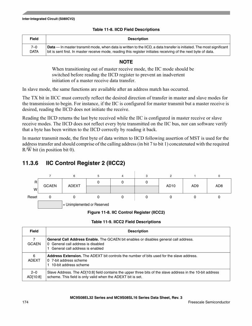
Inter-Integrated Circuit (S08IICV2)
MC9S08EL32 Series and MC9S08SL16 Series Data Sheet, Rev. 3174 Freescale Semiconductor
NOTEWhen transitioning out of master receive mode, the IIC mode should be switched before reading the IICD register to prevent an inadvertent initiation of a master receive data transfer.
In slave mode, the same functions are available after an address match has occurred.
The TX bit in IICC must correctly reflect the desired direction of transfer in master and slave modes for the transmission to begin. For instance, if the IIC is configured for master transmit but a master receive is desired, reading the IICD does not initiate the receive.
Reading the IICD returns the last byte received while the IIC is configured in master receive or slave receive modes. The IICD does not reflect every byte transmitted on the IIC bus, nor can software verify that a byte has been written to the IICD correctly by reading it back.
In master transmit mode, the first byte of data written to IICD following assertion of MST is used for the address transfer and should comprise of the calling address (in bit 7 to bit 1) concatenated with the required R/W bit (in position bit 0).
11.3.6 IIC Control Register 2 (IICC2)
Table 11-8. IICD Field Descriptions
Field Description
7–0DATA
Data — In master transmit mode, when data is written to the IICD, a data transfer is initiated. The most significant bit is sent first. In master receive mode, reading this register initiates receiving of the next byte of data.
7 6 5 4 3 2 1 0
RGCAEN ADEXT
0 0 0AD10 AD9 AD8
W
Reset 0 0 0 0 0 0 0 0
= Unimplemented or Reserved
Figure 11-8. IIC Control Register (IICC2)
Table 11-9. IICC2 Field Descriptions
Field Description
7GCAEN
General Call Address Enable. The GCAEN bit enables or disables general call address.0 General call address is disabled1 General call address is enabled
6ADEXT
Address Extension. The ADEXT bit controls the number of bits used for the slave address.0 7-bit address scheme1 10-bit address scheme
2–0AD[10:8]
Slave Address. The AD[10:8] field contains the upper three bits of the slave address in the 10-bit address scheme. This field is only valid when the ADEXT bit is set.
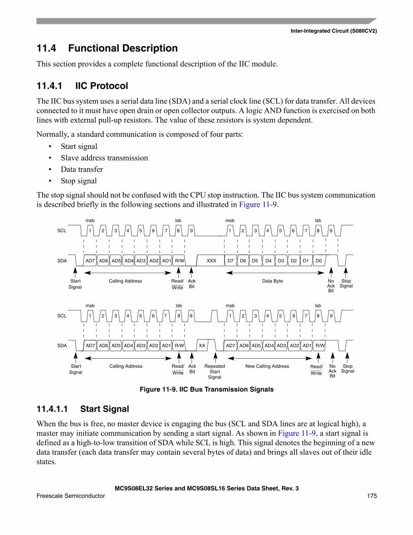
Inter-Integrated Circuit (S08IICV2)
MC9S08EL32 Series and MC9S08SL16 Series Data Sheet, Rev. 3Freescale Semiconductor 175
11.4 Functional DescriptionThis section provides a complete functional description of the IIC module.
11.4.1 IIC Protocol
The IIC bus system uses a serial data line (SDA) and a serial clock line (SCL) for data transfer. All devices connected to it must have open drain or open collector outputs. A logic AND function is exercised on both lines with external pull-up resistors. The value of these resistors is system dependent.
Normally, a standard communication is composed of four parts: • Start signal• Slave address transmission• Data transfer• Stop signal
The stop signal should not be confused with the CPU stop instruction. The IIC bus system communication is described briefly in the following sections and illustrated in Figure 11-9.
Figure 11-9. IIC Bus Transmission Signals
11.4.1.1 Start Signal
When the bus is free, no master device is engaging the bus (SCL and SDA lines are at logical high), a master may initiate communication by sending a start signal. As shown in Figure 11-9, a start signal is defined as a high-to-low transition of SDA while SCL is high. This signal denotes the beginning of a new data transfer (each data transfer may contain several bytes of data) and brings all slaves out of their idle states.
SCL
SDA
StartSignal
AckBit
1 2 3 4 5 6 7 8
msb lsb
1 2 3 4 5 6 7 8
msb lsb
StopSignal
No
SCL
SDA
1 2 3 4 5 6 7 8
msb lsb
1 2 5 6 7 8
msb lsb
Repeated
3 4
9 9
AD7 AD6 AD5 AD4 AD3 AD2 AD1 R/W XXX D7 D6 D5 D4 D3 D2 D1 D0
Calling Address Read/ Data Byte
AD7 AD6 AD5 AD4 AD3 AD2 AD1 R/W AD7 AD6 AD5 AD4 AD3 AD2 AD1 R/W
New Calling Address
9 9
XX
AckBit
Write
StartSignal
StartSignal
AckBit
Calling Address Read/Write
StopSignal
NoAckBit
Read/Write
Inter-Integrated Circuit (S08IICV2)
MC9S08EL32 Series and MC9S08SL16 Series Data Sheet, Rev. 3176 Freescale Semiconductor
11.4.1.2 Slave Address Transmission
The first byte of data transferred immediately after the start signal is the slave address transmitted by the master. This is a seven-bit calling address followed by a R/W bit. The R/W bit tells the slave the desired direction of data transfer.
1 = Read transfer, the slave transmits data to the master.0 = Write transfer, the master transmits data to the slave.
Only the slave with a calling address that matches the one transmitted by the master responds by sending back an acknowledge bit. This is done by pulling the SDA low at the ninth clock (see Figure 11-9).
No two slaves in the system may have the same address. If the IIC module is the master, it must not transmit an address equal to its own slave address. The IIC cannot be master and slave at the same time. However, if arbitration is lost during an address cycle, the IIC reverts to slave mode and operates correctly even if it is being addressed by another master.
11.4.1.3 Data Transfer
Before successful slave addressing is achieved, the data transfer can proceed byte-by-byte in a direction specified by the R/W bit sent by the calling master.
All transfers that come after an address cycle are referred to as data transfers, even if they carry sub-address information for the slave device
Each data byte is 8 bits long. Data may be changed only while SCL is low and must be held stable while SCL is high as shown in Figure 11-9. There is one clock pulse on SCL for each data bit, the msb being transferred first. Each data byte is followed by a 9th (acknowledge) bit, which is signalled from the receiving device. An acknowledge is signalled by pulling the SDA low at the ninth clock. In summary, one complete data transfer needs nine clock pulses.
If the slave receiver does not acknowledge the master in the ninth bit time, the SDA line must be left high by the slave. The master interprets the failed acknowledge as an unsuccessful data transfer.
If the master receiver does not acknowledge the slave transmitter after a data byte transmission, the slave interprets this as an end of data transfer and releases the SDA line.
In either case, the data transfer is aborted and the master does one of two things:• Relinquishes the bus by generating a stop signal.• Commences a new calling by generating a repeated start signal.
11.4.1.4 Stop Signal
The master can terminate the communication by generating a stop signal to free the bus. However, the master may generate a start signal followed by a calling command without generating a stop signal first. This is called repeated start. A stop signal is defined as a low-to-high transition of SDA while SCL at logical 1 (see Figure 11-9).
The master can generate a stop even if the slave has generated an acknowledge at which point the slave must release the bus.
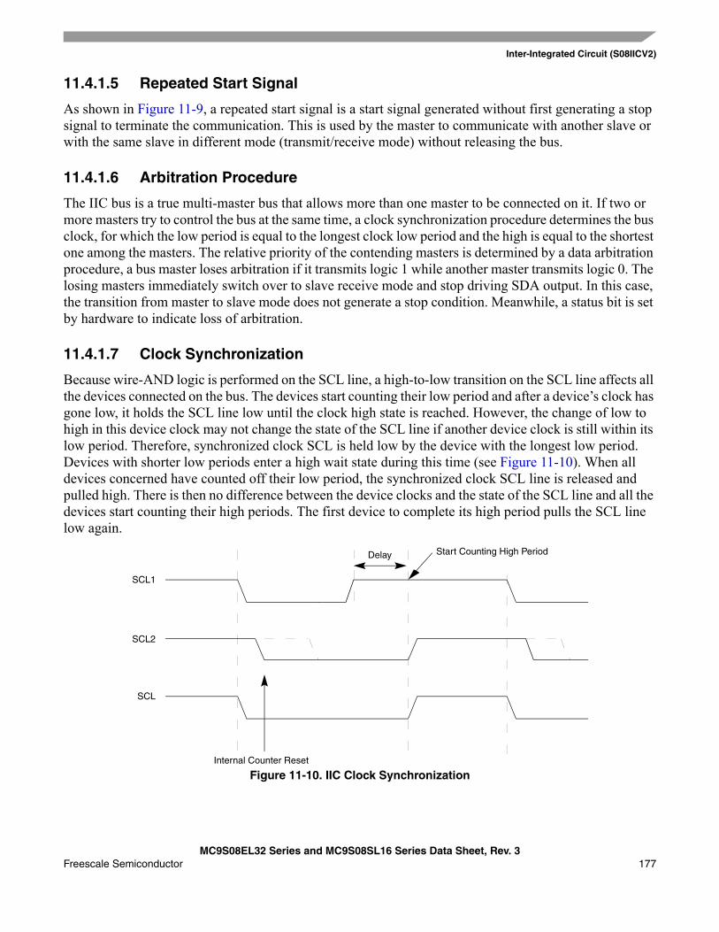
Inter-Integrated Circuit (S08IICV2)
MC9S08EL32 Series and MC9S08SL16 Series Data Sheet, Rev. 3Freescale Semiconductor 177
11.4.1.5 Repeated Start Signal
As shown in Figure 11-9, a repeated start signal is a start signal generated without first generating a stop signal to terminate the communication. This is used by the master to communicate with another slave or with the same slave in different mode (transmit/receive mode) without releasing the bus.
11.4.1.6 Arbitration Procedure
The IIC bus is a true multi-master bus that allows more than one master to be connected on it. If two or more masters try to control the bus at the same time, a clock synchronization procedure determines the bus clock, for which the low period is equal to the longest clock low period and the high is equal to the shortest one among the masters. The relative priority of the contending masters is determined by a data arbitration procedure, a bus master loses arbitration if it transmits logic 1 while another master transmits logic 0. The losing masters immediately switch over to slave receive mode and stop driving SDA output. In this case, the transition from master to slave mode does not generate a stop condition. Meanwhile, a status bit is set by hardware to indicate loss of arbitration.
11.4.1.7 Clock Synchronization
Because wire-AND logic is performed on the SCL line, a high-to-low transition on the SCL line affects all the devices connected on the bus. The devices start counting their low period and after a device’s clock has gone low, it holds the SCL line low until the clock high state is reached. However, the change of low to high in this device clock may not change the state of the SCL line if another device clock is still within its low period. Therefore, synchronized clock SCL is held low by the device with the longest low period. Devices with shorter low periods enter a high wait state during this time (see Figure 11-10). When all devices concerned have counted off their low period, the synchronized clock SCL line is released and pulled high. There is then no difference between the device clocks and the state of the SCL line and all the devices start counting their high periods. The first device to complete its high period pulls the SCL line low again.
Figure 11-10. IIC Clock Synchronization
SCL1
SCL2
SCL
Internal Counter Reset
Delay Start Counting High Period
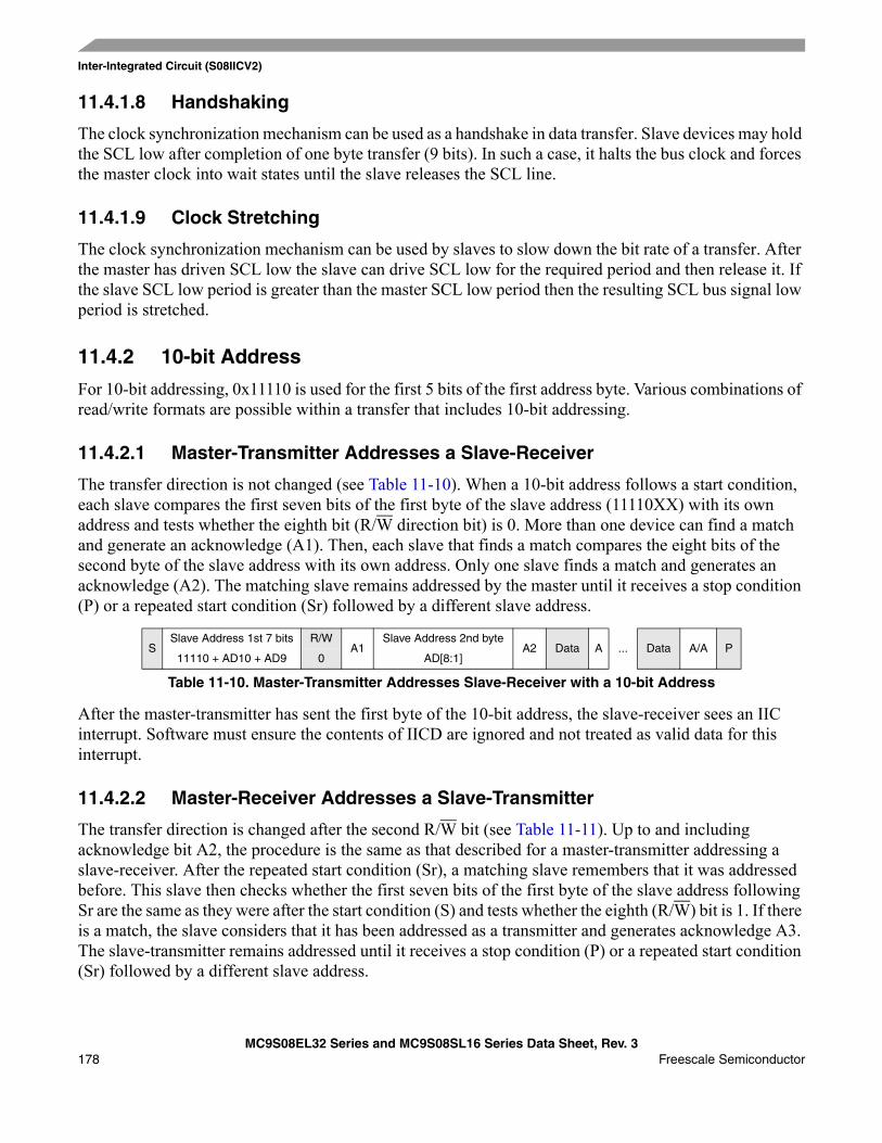
Inter-Integrated Circuit (S08IICV2)
MC9S08EL32 Series and MC9S08SL16 Series Data Sheet, Rev. 3178 Freescale Semiconductor
11.4.1.8 Handshaking
The clock synchronization mechanism can be used as a handshake in data transfer. Slave devices may hold the SCL low after completion of one byte transfer (9 bits). In such a case, it halts the bus clock and forces the master clock into wait states until the slave releases the SCL line.
11.4.1.9 Clock Stretching
The clock synchronization mechanism can be used by slaves to slow down the bit rate of a transfer. After the master has driven SCL low the slave can drive SCL low for the required period and then release it. If the slave SCL low period is greater than the master SCL low period then the resulting SCL bus signal low period is stretched.
11.4.2 10-bit Address
For 10-bit addressing, 0x11110 is used for the first 5 bits of the first address byte. Various combinations of read/write formats are possible within a transfer that includes 10-bit addressing.
11.4.2.1 Master-Transmitter Addresses a Slave-Receiver
The transfer direction is not changed (see Table 11-10). When a 10-bit address follows a start condition, each slave compares the first seven bits of the first byte of the slave address (11110XX) with its own address and tests whether the eighth bit (R/W direction bit) is 0. More than one device can find a match and generate an acknowledge (A1). Then, each slave that finds a match compares the eight bits of the second byte of the slave address with its own address. Only one slave finds a match and generates an acknowledge (A2). The matching slave remains addressed by the master until it receives a stop condition (P) or a repeated start condition (Sr) followed by a different slave address.
After the master-transmitter has sent the first byte of the 10-bit address, the slave-receiver sees an IIC interrupt. Software must ensure the contents of IICD are ignored and not treated as valid data for this interrupt.
11.4.2.2 Master-Receiver Addresses a Slave-Transmitter
The transfer direction is changed after the second R/W bit (see Table 11-11). Up to and including acknowledge bit A2, the procedure is the same as that described for a master-transmitter addressing a slave-receiver. After the repeated start condition (Sr), a matching slave remembers that it was addressed before. This slave then checks whether the first seven bits of the first byte of the slave address following Sr are the same as they were after the start condition (S) and tests whether the eighth (R/W) bit is 1. If there is a match, the slave considers that it has been addressed as a transmitter and generates acknowledge A3. The slave-transmitter remains addressed until it receives a stop condition (P) or a repeated start condition (Sr) followed by a different slave address.
SSlave Address 1st 7 bits R/W
A1Slave Address 2nd byte
A2 Data A ... Data A/A P11110 + AD10 + AD9 0 AD[8:1]
Table 11-10. Master-Transmitter Addresses Slave-Receiver with a 10-bit Address
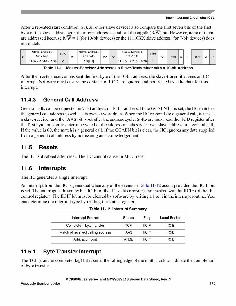
Inter-Integrated Circuit (S08IICV2)
MC9S08EL32 Series and MC9S08SL16 Series Data Sheet, Rev. 3Freescale Semiconductor 179
After a repeated start condition (Sr), all other slave devices also compare the first seven bits of the first byte of the slave address with their own addresses and test the eighth (R/W) bit. However, none of them are addressed because R/W = 1 (for 10-bit devices) or the 11110XX slave address (for 7-bit devices) does not match.
After the master-receiver has sent the first byte of the 10-bit address, the slave-transmitter sees an IIC interrupt. Software must ensure the contents of IICD are ignored and not treated as valid data for this interrupt.
11.4.3 General Call Address
General calls can be requested in 7-bit address or 10-bit address. If the GCAEN bit is set, the IIC matches the general call address as well as its own slave address. When the IIC responds to a general call, it acts as a slave-receiver and the IAAS bit is set after the address cycle. Software must read the IICD register after the first byte transfer to determine whether the address matches is its own slave address or a general call. If the value is 00, the match is a general call. If the GCAEN bit is clear, the IIC ignores any data supplied from a general call address by not issuing an acknowledgement.
11.5 ResetsThe IIC is disabled after reset. The IIC cannot cause an MCU reset.
11.6 InterruptsThe IIC generates a single interrupt.
An interrupt from the IIC is generated when any of the events in Table 11-12 occur, provided the IICIE bit is set. The interrupt is driven by bit IICIF (of the IIC status register) and masked with bit IICIE (of the IIC control register). The IICIF bit must be cleared by software by writing a 1 to it in the interrupt routine. You can determine the interrupt type by reading the status register.
11.6.1 Byte Transfer Interrupt
The TCF (transfer complete flag) bit is set at the falling edge of the ninth clock to indicate the completion of byte transfer.
S
Slave Address1st 7 bits
R/WA1
Slave Address2nd byte A2 Sr
Slave Address1st 7 bits
R/WA3 Data A ... Data A P
11110 + AD10 + AD9 0 AD[8:1] 11110 + AD10 + AD9 1
Table 11-11. Master-Receiver Addresses a Slave-Transmitter with a 10-bit Address
Table 11-12. Interrupt Summary
Interrupt Source Status Flag Local Enable
Complete 1-byte transfer TCF IICIF IICIE
Match of received calling address IAAS IICIF IICIE
Arbitration Lost ARBL IICIF IICIE
Inter-Integrated Circuit (S08IICV2)
MC9S08EL32 Series and MC9S08SL16 Series Data Sheet, Rev. 3180 Freescale Semiconductor
11.6.2 Address Detect Interrupt
When the calling address matches the programmed slave address (IIC address register) or when the GCAEN bit is set and a general call is received, the IAAS bit in the status register is set. The CPU is interrupted, provided the IICIE is set. The CPU must check the SRW bit and set its Tx mode accordingly.
11.6.3 Arbitration Lost Interrupt
The IIC is a true multi-master bus that allows more than one master to be connected on it. If two or more masters try to control the bus at the same time, the relative priority of the contending masters is determined by a data arbitration procedure. The IIC module asserts this interrupt when it loses the data arbitration process and the ARBL bit in the status register is set.
Arbitration is lost in the following circumstances:• SDA sampled as a low when the master drives a high during an address or data transmit cycle.• SDA sampled as a low when the master drives a high during the acknowledge bit of a data receive
cycle.• A start cycle is attempted when the bus is busy.• A repeated start cycle is requested in slave mode.• A stop condition is detected when the master did not request it.
This bit must be cleared by software writing a 1 to it.
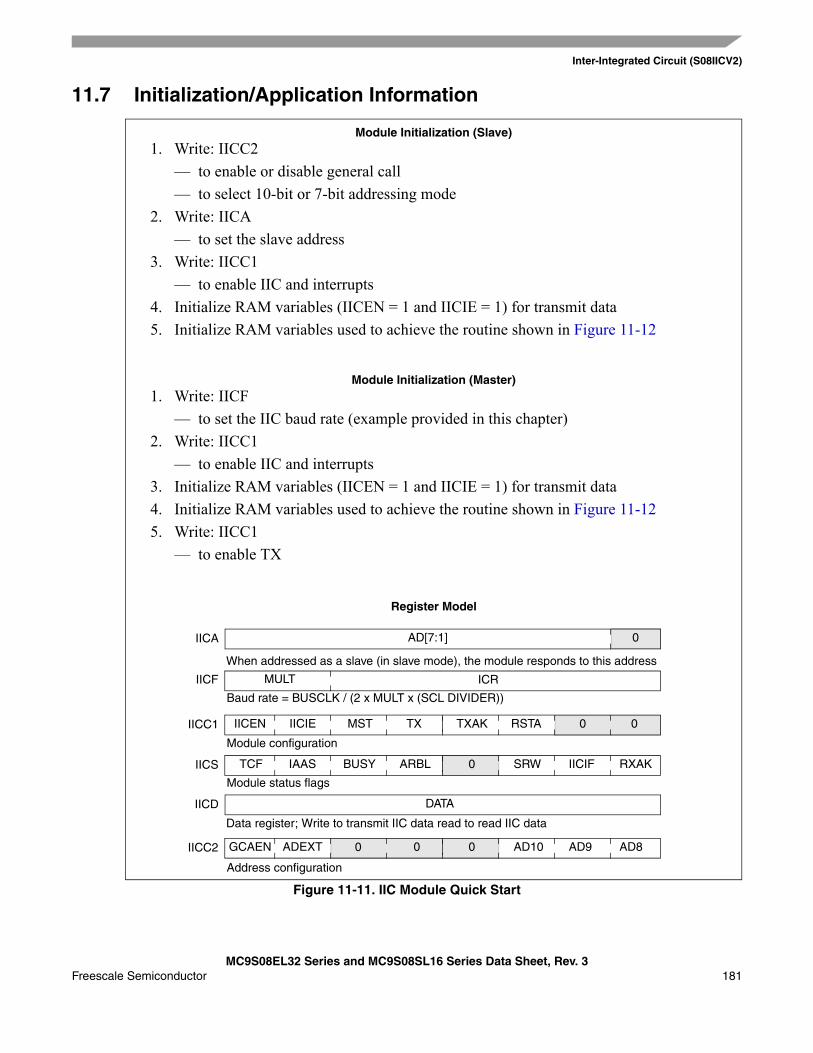
Inter-Integrated Circuit (S08IICV2)
MC9S08EL32 Series and MC9S08SL16 Series Data Sheet, Rev. 3Freescale Semiconductor 181
11.7 Initialization/Application Information
Figure 11-11. IIC Module Quick Start
Module Initialization (Slave)1. Write: IICC2
— to enable or disable general call— to select 10-bit or 7-bit addressing mode
2. Write: IICA— to set the slave address
3. Write: IICC1— to enable IIC and interrupts
4. Initialize RAM variables (IICEN = 1 and IICIE = 1) for transmit data5. Initialize RAM variables used to achieve the routine shown in Figure 11-12
Module Initialization (Master)1. Write: IICF
— to set the IIC baud rate (example provided in this chapter)2. Write: IICC1
— to enable IIC and interrupts3. Initialize RAM variables (IICEN = 1 and IICIE = 1) for transmit data4. Initialize RAM variables used to achieve the routine shown in Figure 11-125. Write: IICC1
— to enable TX
0
IICF
IICA
Baud rate = BUSCLK / (2 x MULT x (SCL DIVIDER))
TX TXAK RSTA 0 0IICC1 IICEN IICIE MST
Module configuration
ARBL 0 SRW IICIF RXAKIICS TCF IAAS BUSY
Module status flags
Register Model
AD[7:1]
When addressed as a slave (in slave mode), the module responds to this address
MULT ICR
IICD DATA
Data register; Write to transmit IIC data read to read IIC data
0 AD10 AD9 AD8IICC2 GCAEN ADEXT
Address configuration
00
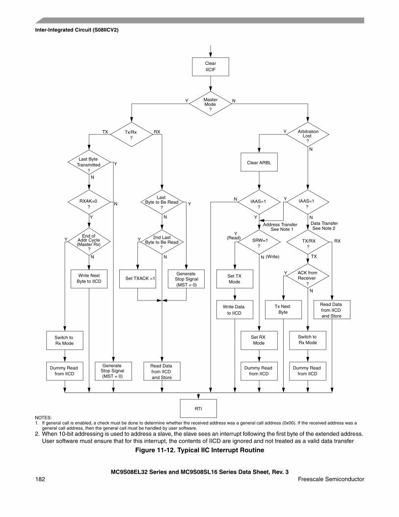
Inter-Integrated Circuit (S08IICV2)
MC9S08EL32 Series and MC9S08SL16 Series Data Sheet, Rev. 3182 Freescale Semiconductor
Figure 11-12. Typical IIC Interrupt Routine
Clear
Master Mode
?
Tx/Rx ?
Last Byte Transmitted
?
RXAK=0 ?
End of Addr Cycle (Master Rx)
?
Write NextByte to IICD
Switch to Rx Mode
Dummy Read from IICD
Generate Stop Signal
Read Data from IICD and Store
Set TXACK =1Generate
Stop Signal
2nd Last Byte to Be Read
?
Last Byte to Be Read
?
Arbitration Lost
?
Clear ARBL
IAAS=1 ?
IAAS=1 ?
SRW=1 ?
TX/RX ?
Set TX Mode
Write Data to IICD
Set RX Mode
Dummy Read from IICD
ACK fromReceiver
?
Tx Next Byte
Read Data from IICD and Store
Switch to Rx Mode
Dummy Read from IICD
RTI
Y N
Y
Y Y
Y
Y
Y
Y
Y
Y
N
N
N
NN
N
N
N
N
Y
TX RX
RX
TX(Write)
(Read)
N
IICIF
Address Transfer Data Transfer
(MST = 0)
(MST = 0)
See Note 1
NOTES:1. If general call is enabled, a check must be done to determine whether the received address was a general call address (0x00). If the received address was a
general call address, then the general call must be handled by user software.2. When 10-bit addressing is used to address a slave, the slave sees an interrupt following the first byte of the extended address.
User software must ensure that for this interrupt, the contents of IICD are ignored and not treated as a valid data transfer
See Note 2
MC9S08EL32 Series and MC9S08SL16 Series Data Sheet, Rev. 3
Freescale Semiconductor 185
Chapter 12 Slave LIN Interface Controller (S08SLICV1)
12.1 IntroductionThe slave LIN interface controller (SLIC) is designed to provide slave node connectivity on a local interconnect network (LIN) sub-bus. LIN is an open-standard serial protocol developed for the automotive industry to connect sensors, motors, and actuators.
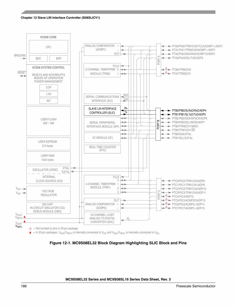
Chapter 12 Slave LIN Interface Controller (S08SLICV1)
MC9S08EL32 Series and MC9S08SL16 Series Data Sheet, Rev. 3
186 Freescale Semiconductor
Figure 12-1. MC9S08EL32 Block Diagram Highlighting SLIC Block and Pins
VSS
IIC MODULE (IIC)
SERIAL PERIPHERAL INTERFACE MODULE (SPI)
USER FLASH
USER RAM
32K / 16K
HCS08 CORE
CPU
BDC
2-CHANNEL TIMER/PWMMODULE (TPM2)
HCS08 SYSTEM CONTROL
RESETS AND INTERRUPTSMODES OF OPERATIONPOWER MANAGEMENT
VOLTAGE REGULATOR
COP
LVD
OSCILLATOR (XOSC)
INTERNALCLOCK SOURCE (ICS)
RESET
VREFH
1024 bytes
INTERFACE (SCI)SERIAL COMMUNICATIONS
XTALEXTAL
4-CHANNEL TIMER/PWMMODULE (TPM1)
REAL-TIME COUNTER
IN-CIRCUIT EMULATOR (ICE)
BKGD/MS PTA3/PIA3/SCL/TxD/ADP3
PTA6/TPM2CH0
PTA2/PIA2/SDA/RxD/ACMP1O/ADP2PTA1/PIA1/TPM2CH0/ACMP1–/ADP1PTA0/PIA0/TPM1CH0/TCLK/ACMP1+/ADP0
PTA7/TPM2CH1
PTB3/PIB3/SCL/MOSI/ADP7PTB4/TPM2CH1/MISO
PTB2/PIB2/SDA/SPSCK/ADP6PTB1/PIB1/SLTxD/TxD/ADP5PTB0/PIB0/SLRxD/RxD/ADP4
PTB7/SCL/EXTAL
PTC3/PIC3/TPM1CH3/ADP11PTC4/PIC4/ADP12PTC5/PIC5/ACMP2O/ADP13
PTC2/PIC2/TPM1CH2/ADP10PTC1/PIC1/TPM1CH1/ADP9
POR
T C
PTC6/PIC6/ACMP2+/ADP14
VDD
BKP
INT
ANALOG COMPARATOR(ACMP2)
USER EEPROM512 bytes
CONTROLLER (SLIC)SLAVE LIN INTERFACE
ANALOG-TO-DIGITALCONVERTER (ADC)
16-CHANNEL,10-BIT16
= In 20-pin packages, VDDA/VREFH is internally connected to VDD and VSSA/VREFL is internally connected to VSS.
VDDA/
VREFL
VSSA/
DEBUG MODULE (DBG)
ON-CHIP
(RTC)
PTC0/PIC0/TPM1CH0/ADP8
PTC7/PIC7/ACMP2–/ADP15
PTB6/SDA/XTAL
POR
T B
POR
T A
PTB5/TPM1CH1/SS
ANALOG COMPARATOR(ACMP1)
= Not bonded to pins in 20-pin package
TCLK
TCLK
+–
OUT
+–
OUT
0123
10
RxDTxD
TxRx
MC9S08EL32 Series and MC9S08SL16 Series Data Sheet, Rev. 3
Freescale Semiconductor 187
12.1.1 Features
The SLIC includes these distinctive features:• Full LIN message buffering of identifier and 8 data bytes• Automatic bit rate and LIN message frame synchronization:
— No prior programming of bit rate required, 1–20 kbps LIN bus speed operation— All LIN messages will be received (no message loss due to synchronization process)— Input clock tolerance as high as ±50%, allowing internal oscillator to remain untrimmed— Incoming break symbols always allowed to be 10 or more bit times without message loss— Supports automatic software trimming of internal oscillator using LIN synchronization data
• Automatic processing and verification of LIN SYNCH BREAK and SYNCH BYTE• Automatic checksum calculation and verification with error reporting • Maximum of two interrupts per standard LIN message frame with no errors • Full LIN error checking and reporting• High-speed LIN capability up to 83.33 kbps to 120.00 kbps1
• Configurable digital receive filter • Streamlined interrupt servicing through use of a state vector register • Switchable UART-like byte transfer mode for processing bytes one at a time without LIN message
framing constraints• Enhanced checksum (includes ID) generation and verification
1. Maximum bit rate of SLIC module dependent upon frequency of SLIC input clock.
MC9S08EL32 Series and MC9S08SL16 Series Data Sheet, Rev. 3
188 Freescale Semiconductor
12.1.2 Modes of Operation
Figure 12-2 shows the modes in which the SLIC will operate.
Figure 12-2. SLIC Operating Modes
12.1.2.1 Power Off
This mode is entered from the reset mode whenever the SLIC module supply voltage VDD drops below its minimum specified value for the SLIC module to guarantee operation. The SLIC module will be placed in the reset mode by a system low-voltage reset (LVR) before being powered down. In this mode, the pin input and output specifications are not guaranteed.
12.1.2.2 Reset
This mode is entered from the power off mode whenever the SLIC module supply voltage VDD rises above its minimum specified value (VDD(MIN)) and some MCU reset source is asserted. To prevent the SLIC from entering an unknown state, the internal MCU reset is asserted while powering up the SLIC module. SLIC reset mode is also entered from any other mode as soon as one of the MCU's possible reset sources (e.g., LVR, POR, COP, RST pin, etc.) is asserted. SLIC reset mode may also be entered by the user software by asserting the INITREQ bit. INITACK indicates whether the SLIC module is in the reset mode as a result of writing INITREQ in SLCC1. While in the reset state the SLIC module clocks are stopped. Clearing the INITREQ allows the SLIC to proceed and enter SLIC run mode (if SLCE is set). The module
VDD > VDD (MIN) AND ANY
SLIC RESET
SLIC DISABLED
SLIC RUN
SLIC INITREQUESTED
SLIC STOP SLIC WAIT
MCU RESET SOURCE ASSERTED
POWER OFF
NO MCU RESET SOURCE ASSERTED
SLCE SET IN SLCC2 REGISTER
NETWORK ACTIVITY OR OTHERMCU WAKEUP
(WAIT INSTRUCTIONAND SLCWCM = 0)STOP INSTRUCTION
(WAIT INSTRUCTION AND SLCWCM = 1)
SLCIE=1 and NETWORK ACTIVITYOR OTHER MCU
WAKEUP
SLCE CLEARED IN SLCC2 REGISTER
(INITACK = 1)
(FROM ANY MODE)INITREQ SET TO 1 IN
SLCC1 REGISTER
(FROM ANY MODE)ANY MCU RESET SOURCE
ASSERTED
VDD <= VDD (MIN)
INITREQ = 0; (INITACK = 0)
MC9S08EL32 Series and MC9S08SL16 Series Data Sheet, Rev. 3
Freescale Semiconductor 189
will clear INITACK after the module has left reset mode and the SLIC will seek the next LIN header. It is the responsibility of the user to verify that this operation is compatible with the application before implementing this feature.
In this mode, the internal SLIC module voltage references are operative, VDD is supplied to the internal circuits, which are held in their reset state and the internal SLIC module system clock is running. Registers will assume their reset condition. Outputs are held in their programmed reset state, inputs and network activity are ignored.
12.1.2.3 SLIC Disabled
This mode is entered from the reset mode after all MCU reset sources are no longer asserted or INITREQ is cleared by the user and the SLIC module clears INITACK. It is entered from the run mode whenever SLCE in SLCC2 is cleared. In this mode the SLIC clock is stopped to conserve power and allow the SLIC module to be configured for proper operation on the LIN bus.
12.1.2.4 SLIC Run
This mode is entered from the SLIC disabled mode when SLCE in SLCC2 is set. It is entered from the SLIC wait mode whenever activity is sensed on the LIN bus or some other MCU source wakes the CPU out of wait mode.
It is entered from the SLIC stop mode whenever network activity is sensed or some other MCU source wakes the CPU out of stop mode. Messages will not be received properly until the clocks have stabilized and the CPU is also in the run mode.
12.1.2.5 SLIC Wait
This power conserving mode is automatically entered from the run mode whenever the CPU executes a WAIT instruction and SLCWCM in SLCC1 is previously cleared. In this mode, the SLIC module internal clocks continue to run. Any activity on the LIN network will cause the SLIC module to exit SLIC wait mode and return to SLIC run. No activity for an a time on the LIN bus will also cause the No Bus Activity Interrupt source to occur. This will also cause an exit from SLIC wait mode.
12.1.2.6 Wakeup from SLIC Wait with CPU in WAIT
If the CPU executes the WAIT instruction and the SLIC module enters the wait mode (SLCWCM = 0), the clocks to the SLIC module as well as the clocks in the MCU continue to run. Therefore, the message that wakes up the SLIC module from WAIT and the CPU from wait mode will also be received correctly by the SLIC module. This is because all of the required clocks continue to run in the SLIC module in wait mode.
12.1.2.7 SLIC Stop
This power conserving mode is automatically entered from the run mode whenever the CPU executes a STOP instruction, or if the CPU executes a WAIT instruction and SLCWCM in SLCC1 is previously set. In this mode, the SLIC internal clocks are stopped. If SLIC interrupts are enabled (SLCIE = 1) prior to
MC9S08EL32 Series and MC9S08SL16 Series Data Sheet, Rev. 3
190 Freescale Semiconductor
entering SLIC stop mode, any activity on the network will cause the SLIC module to exit SLIC stop mode and generate an unmaskable interrupt of the CPU. This wakeup interrupt state is reflected in the SLCSV, encoded as the highest priority interrupt. This interrupt can be cleared by the CPU with a read of the SLCSV and clearing of the SLCF interrupt flag. Depending upon which low-power mode instruction the CPU executes to cause the SLIC module to enter SLIC stop, the message which wakes up the SLIC module (and the CPU) may or may not be received.
There are two different possibilities: 1. Wakeup from SLIC Stop with CPU in STOP
When the CPU executes the STOP instruction, all clocks in the MCU, including clocks to the SLIC module, are turned off. Therefore, the message which wakes up the SLIC module and the CPU from stop mode will not be received. This is due primarily to the amount of time required for the MCU's oscillator to stabilize before the clocks can be applied internally to the other MCU modules, including the SLIC module.
2. Wakeup from SLIC Stop with CPU in WAIT. If the CPU executes the WAIT instruction and the SLIC module enters the stop mode (SLCWCM = 1), the clocks to the SLIC module are turned off, but the clocks in the MCU continue to run. Therefore, the message which wakes up the SLIC module from stop and the CPU from wait mode will be received correctly by the SLIC module. This is because very little time is required for the CPU to turn the clocks to the SLIC module back on after the wakeup interrupt occurs.
NOTEWhile the SLIC module will correctly receive a message which arrives when the SLIC module is in stop or wait mode and the MCU is in wait mode, if the user enters this mode while a message is being received, the data in the message will become corrupted. This is due to the steps required for the SLIC module to resume operation upon exiting stop or wait mode, and its subsequent resynchronization with the LIN bus.
12.1.2.8 Normal and Emulation Mode Operation
The SLIC module operates in the same manner in all normal and emulation modes. All SLIC module registers can be read and written except those that are reserved, unimplemented, or write once. The user must be careful not to unintentionally change reserved bits to avoid unexpected SLIC module behavior.
12.1.2.9 Special Mode Operation
Some aspects of SLIC module operation can be modified in special test mode. This mode is reserved for internal use only.
12.1.2.10 Low-Power Options
The SLIC module can save power in disabled, wait, and stop modes.
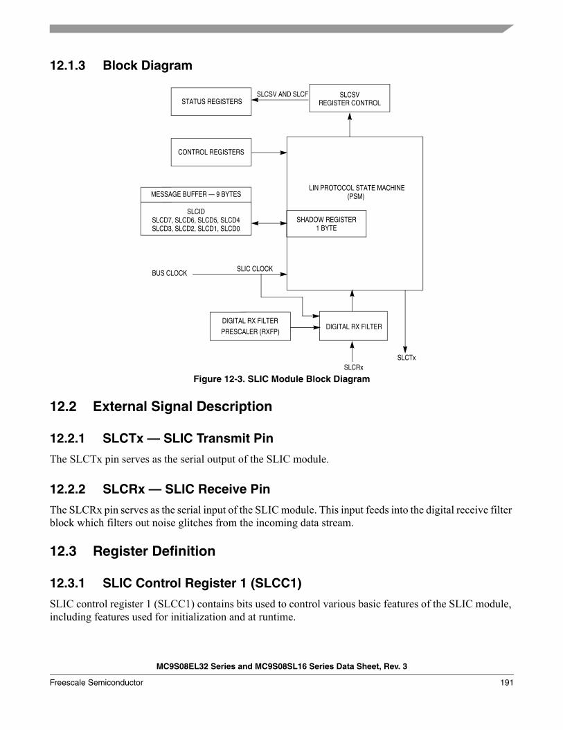
MC9S08EL32 Series and MC9S08SL16 Series Data Sheet, Rev. 3
Freescale Semiconductor 191
12.1.3 Block Diagram
Figure 12-3. SLIC Module Block Diagram
12.2 External Signal Description
12.2.1 SLCTx — SLIC Transmit Pin
The SLCTx pin serves as the serial output of the SLIC module.
12.2.2 SLCRx — SLIC Receive Pin
The SLCRx pin serves as the serial input of the SLIC module. This input feeds into the digital receive filter block which filters out noise glitches from the incoming data stream.
12.3 Register Definition
12.3.1 SLIC Control Register 1 (SLCC1)
SLIC control register 1 (SLCC1) contains bits used to control various basic features of the SLIC module, including features used for initialization and at runtime.
STATUS REGISTERS
CONTROL REGISTERS
BUS CLOCK
MESSAGE BUFFER — 9 BYTES
SLCIDSLCD7, SLCD6, SLCD5, SLCD4 SHADOW REGISTER
1 BYTE
LIN PROTOCOL STATE MACHINE(PSM)
DIGITAL RX FILTER
SLCRxSLCTx
SLCSVSLCSV AND SLCF
DIGITAL RX FILTER
PRESCALER (RXFP)
SLIC CLOCK
SLCD3, SLCD2, SLCD1, SLCD0
REGISTER CONTROL
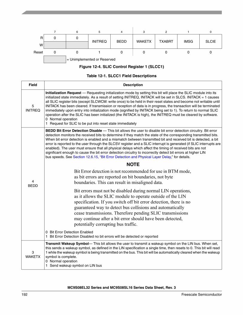
MC9S08EL32 Series and MC9S08SL16 Series Data Sheet, Rev. 3
192 Freescale Semiconductor
7 6 5 4 3 2 1 0
R 0 0INITREQ BEDD WAKETX TXABRT IMSG SLCIE
W
Reset 0 0 1 0 0 0 0 0
= Unimplemented or Reserved
Figure 12-4. SLIC Control Register 1 (SLCC1)
Table 12-1. SLCC1 Field Descriptions
Field Description
5INITREQ
Initialization Request — Requesting initialization mode by setting this bit will place the SLIC module into its initialized state immediately. As a result of setting INITREQ, INITACK will be set in SLCS. INITACK = 1 causes all SLIC register bits (except SLCWCM: write once) to be held in their reset states and become not writable until INITACK has been cleared. If transmission or reception of data is in progress, the transaction will be terminated immediately upon entry into initialization mode (signified by INITACK being set to 1). To return to normal SLIC operation after the SLIC has been initialized (the INITACK is high), the INITREQ must be cleared by software.0 Normal operation1 Request for SLIC to be put into reset state immediately
4BEDD
BEDD Bit Error Detection Disable — This bit allows the user to disable bit error detection circuitry. Bit error detection monitors the received bits to determine if they match the state of the corresponding transmitted bits. When bit error detection is enabled and a mismatch between transmitted bit and received bit is detected, a bit error is reported to the user through the SLCSV register and a SLIC interrupt is generated (if SLIC interrupts areenabled). The user must ensure that all physical delays which affect the timing of received bits are notsignificant enough to cause the bit error detection circuitry to incorrectly detect bit errors at higher LINbus speeds. See Section 12.6.15, “Bit Error Detection and Physical Layer Delay,” for details.
NOTEBit Error detection is not recommended for use in BTM mode, as bit errors are reported on bit boundaries, not byte boundaries. This can result in misaligned data.
Bit errors must not be disabled during normal LIN operations, as it allows the SLIC module to operate outside of the LIN specification. If you switch off bit error detection, there is no guaranteed way to detect bus collisions and automatically cease transmissions. Therefore pending SLIC transmissions may continue after a bit error should have been detected, potentially corrupting bus traffic.
0 Bit Error Detection Enabled1 Bit Error Detection Disabled no bit errors will be detected or reported
3WAKETX
Transmit Wakeup Symbol— This bit allows the user to transmit a wakeup symbol on the LIN bus. When set, this sends a wakeup symbol, as defined in the LIN specification a single time, then resets to 0. This bit will read 1 while the wakeup symbol is being transmitted on the bus. This bit will be automatically cleared when the wakeup symbol is complete.0 Normal operation1 Send wakeup symbol on LIN bus
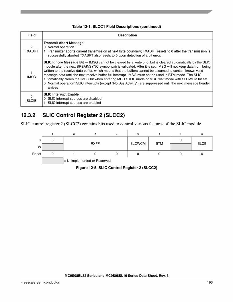
MC9S08EL32 Series and MC9S08SL16 Series Data Sheet, Rev. 3
Freescale Semiconductor 193
12.3.2 SLIC Control Register 2 (SLCC2)
SLIC control register 2 (SLCC2) contains bits used to control various features of the SLIC module.
2TXABRT
Transmit Abort Message0 Normal operation1 Transmitter aborts current transmission at next byte boundary; TXABRT resets to 0 after the transmission is
successfully aborted TXABRT also resets to 0 upon detection of a bit error.
1IMSG
SLIC Ignore Message Bit — IMSG cannot be cleared by a write of 0, but is cleared automatically by the SLIC module after the next BREAK/SYNC symbol pair is validated. After it is set, IMSG will not keep data from being written to the receive data buffer, which means that the buffers cannot be assumed to contain known valid message data until the next receive buffer full interrupt. IMSG must not be used in BTM mode. The SLIC automatically clears the IMSG bit when entering MCU STOP mode or MCU wait mode with SLCWCM bit set.0 Normal operation1SLIC interrupts (except "No Bus Activity") are suppressed until the next message header
arrives
0SLCIE
SLIC Interrupt Enable0 SLIC interrupt sources are disabled 1 SLIC interrupt sources are enabled
7 6 5 4 3 2 1 0
R 0RXFP SLCWCM BTM
0SLCE
W
Reset 0 1 0 0 0 0 0 0
= Unimplemented or Reserved
Figure 12-5. SLIC Control Register 2 (SLCC2)
Table 12-1. SLCC1 Field Descriptions (continued)
Field Description
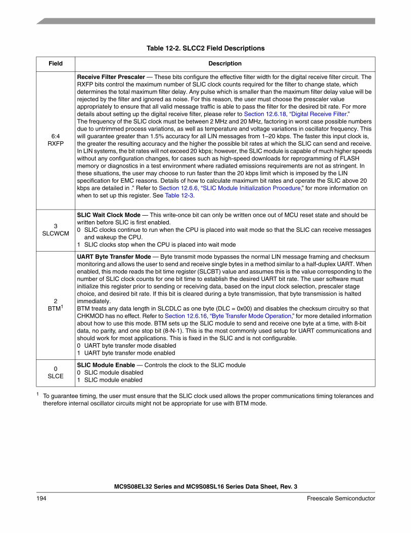
MC9S08EL32 Series and MC9S08SL16 Series Data Sheet, Rev. 3
194 Freescale Semiconductor
Table 12-2. SLCC2 Field Descriptions
Field Description
6:4RXFP
Receive Filter Prescaler — These bits configure the effective filter width for the digital receive filter circuit. The RXFP bits control the maximum number of SLIC clock counts required for the filter to change state, which determines the total maximum filter delay. Any pulse which is smaller than the maximum filter delay value will be rejected by the filter and ignored as noise. For this reason, the user must choose the prescaler value appropriately to ensure that all valid message traffic is able to pass the filter for the desired bit rate. For more details about setting up the digital receive filter, please refer to Section 12.6.18, “Digital Receive Filter.”The frequency of the SLIC clock must be between 2 MHz and 20 MHz, factoring in worst case possible numbers due to untrimmed process variations, as well as temperature and voltage variations in oscillator frequency. This will guarantee greater than 1.5% accuracy for all LIN messages from 1–20 kbps. The faster this input clock is, the greater the resulting accuracy and the higher the possible bit rates at which the SLIC can send and receive. In LIN systems, the bit rates will not exceed 20 kbps; however, the SLIC module is capable of much higher speeds without any configuration changes, for cases such as high-speed downloads for reprogramming of FLASH memory or diagnostics in a test environment where radiated emissions requirements are not as stringent. In these situations, the user may choose to run faster than the 20 kbps limit which is imposed by the LIN specification for EMC reasons. Details of how to calculate maximum bit rates and operate the SLIC above 20 kbps are detailed in .” Refer to Section 12.6.6, “SLIC Module Initialization Procedure,” for more information on when to set up this register. See Table 12-3.
3SLCWCM
SLIC Wait Clock Mode — This write-once bit can only be written once out of MCU reset state and should be written before SLIC is first enabled.0 SLIC clocks continue to run when the CPU is placed into wait mode so that the SLIC can receive messages
and wakeup the CPU.1 SLIC clocks stop when the CPU is placed into wait mode
2BTM1
1 To guarantee timing, the user must ensure that the SLIC clock used allows the proper communications timing tolerances and therefore internal oscillator circuits might not be appropriate for use with BTM mode.
UART Byte Transfer Mode — Byte transmit mode bypasses the normal LIN message framing and checksum monitoring and allows the user to send and receive single bytes in a method similar to a half-duplex UART. When enabled, this mode reads the bit time register (SLCBT) value and assumes this is the value corresponding to the number of SLIC clock counts for one bit time to establish the desired UART bit rate. The user software must initialize this register prior to sending or receiving data, based on the input clock selection, prescaler stage choice, and desired bit rate. If this bit is cleared during a byte transmission, that byte transmission is halted immediately.BTM treats any data length in SLCDLC as one byte (DLC = 0x00) and disables the checksum circuitry so that CHKMOD has no effect. Refer to Section 12.6.16, “Byte Transfer Mode Operation,” for more detailed information about how to use this mode. BTM sets up the SLIC module to send and receive one byte at a time, with 8-bit data, no parity, and one stop bit (8-N-1). This is the most commonly used setup for UART communications and should work for most applications. This is fixed in the SLIC and is not configurable. 0 UART byte transfer mode disabled1 UART byte transfer mode enabled
0SLCE
SLIC Module Enable — Controls the clock to the SLIC module0 SLIC module disabled1 SLIC module enabled
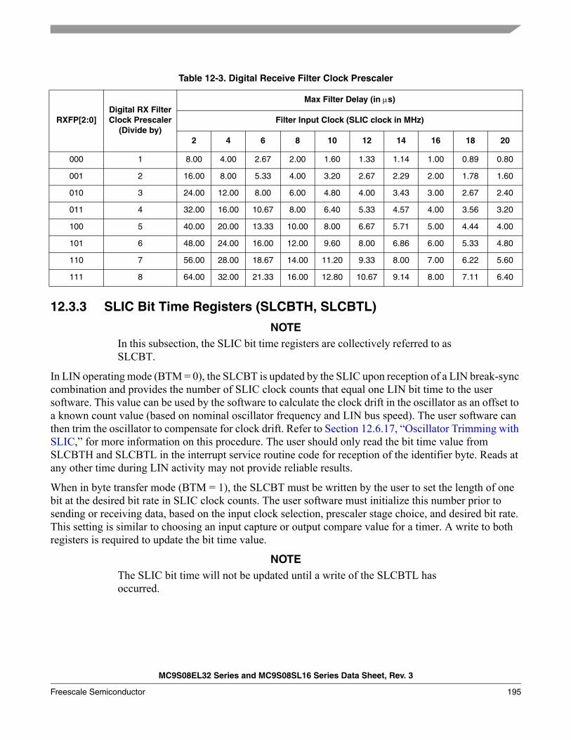
MC9S08EL32 Series and MC9S08SL16 Series Data Sheet, Rev. 3
Freescale Semiconductor 195
12.3.3 SLIC Bit Time Registers (SLCBTH, SLCBTL)
NOTEIn this subsection, the SLIC bit time registers are collectively referred to as SLCBT.
In LIN operating mode (BTM = 0), the SLCBT is updated by the SLIC upon reception of a LIN break-sync combination and provides the number of SLIC clock counts that equal one LIN bit time to the user software. This value can be used by the software to calculate the clock drift in the oscillator as an offset to a known count value (based on nominal oscillator frequency and LIN bus speed). The user software can then trim the oscillator to compensate for clock drift. Refer to Section 12.6.17, “Oscillator Trimming with SLIC,” for more information on this procedure. The user should only read the bit time value from SLCBTH and SLCBTL in the interrupt service routine code for reception of the identifier byte. Reads at any other time during LIN activity may not provide reliable results.
When in byte transfer mode (BTM = 1), the SLCBT must be written by the user to set the length of one bit at the desired bit rate in SLIC clock counts. The user software must initialize this number prior to sending or receiving data, based on the input clock selection, prescaler stage choice, and desired bit rate. This setting is similar to choosing an input capture or output compare value for a timer. A write to both registers is required to update the bit time value.
NOTEThe SLIC bit time will not be updated until a write of the SLCBTL has occurred.
Table 12-3. Digital Receive Filter Clock Prescaler
RXFP[2:0]Digital RX Filter Clock Prescaler
(Divide by)
Max Filter Delay (in μs)
Filter Input Clock (SLIC clock in MHz)
2 4 6 8 10 12 14 16 18 20
000 1 8.00 4.00 2.67 2.00 1.60 1.33 1.14 1.00 0.89 0.80
001 2 16.00 8.00 5.33 4.00 3.20 2.67 2.29 2.00 1.78 1.60
010 3 24.00 12.00 8.00 6.00 4.80 4.00 3.43 3.00 2.67 2.40
011 4 32.00 16.00 10.67 8.00 6.40 5.33 4.57 4.00 3.56 3.20
100 5 40.00 20.00 13.33 10.00 8.00 6.67 5.71 5.00 4.44 4.00
101 6 48.00 24.00 16.00 12.00 9.60 8.00 6.86 6.00 5.33 4.80
110 7 56.00 28.00 18.67 14.00 11.20 9.33 8.00 7.00 6.22 5.60
111 8 64.00 32.00 21.33 16.00 12.80 10.67 9.14 8.00 7.11 6.40
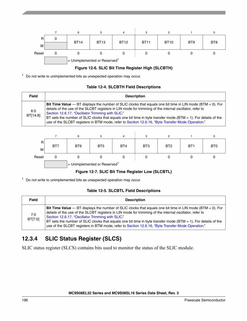
MC9S08EL32 Series and MC9S08SL16 Series Data Sheet, Rev. 3
196 Freescale Semiconductor
12.3.4 SLIC Status Register (SLCS)
SLIC status register (SLCS) contains bits used to monitor the status of the SLIC module.
7 6 5 4 3 2 1 0
R 0BT14 BT13 BT12 BT11 BT10 BT9 BT8
W
Reset 0 0 0 0 0 0 0 0
= Unimplemented or Reserved1
1 Do not write to unimplemented bits as unexpected operation may occur.
Figure 12-6. SLIC Bit Time Register High (SLCBTH)
Table 12-4. SLCBTH Field Descriptions
Field Description
6:0BT[14:8]
Bit Time Value — BT displays the number of SLIC clocks that equals one bit time in LIN mode (BTM = 0). For details of the use of the SLCBT registers in LIN mode for trimming of the internal oscillator, refer to Section 12.6.17, “Oscillator Trimming with SLIC.”BT sets the number of SLIC clocks that equals one bit time in byte transfer mode (BTM = 1). For details of the use of the SLCBT registers in BTM mode, refer to Section 12.6.16, “Byte Transfer Mode Operation.”
7 6 5 4 3 2 1 0
RBT7 BT6 BT5 BT4 BT3 BT2 BT1 BT0
W
Reset 0 0 0 0 0 0 0 0
= Unimplemented or Reserved1
1 Do not write to unimplemented bits as unexpected operation may occur.
Figure 12-7. SLIC Bit Time Register Low (SLCBTL)
Table 12-5. SLCBTL Field Descriptions
Field Description
7:0BT[7:0]
Bit Time Value — BT displays the number of SLIC clocks that equals one bit time in LIN mode (BTM = 0). For details of the use of the SLCBT registers in LIN mode for trimming of the internal oscillator, refer to Section 12.6.17, “Oscillator Trimming with SLIC.”BT sets the number of SLIC clocks that equals one bit time in byte transfer mode (BTM = 1). For details of the use of the SLCBT registers in BTM mode, refer to Section 12.6.16, “Byte Transfer Mode Operation.”
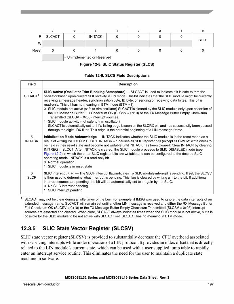
MC9S08EL32 Series and MC9S08SL16 Series Data Sheet, Rev. 3
Freescale Semiconductor 197
12.3.5 SLIC State Vector Register (SLCSV)
SLIC state vector register (SLCSV) is provided to substantially decrease the CPU overhead associated with servicing interrupts while under operation of a LIN protocol. It provides an index offset that is directly related to the LIN module’s current state, which can be used with a user supplied jump table to rapidly enter an interrupt service routine. This eliminates the need for the user to maintain a duplicate state machine in software.
7 6 5 4 3 2 1 0
R SLCACT 0 INITACK 0 0 0 0SLCF
W
Reset 0 0 1 0 0 0 0 0
= Unimplemented or Reserved
Figure 12-8. SLIC Status Register (SLCS)
Table 12-6. SLCS Field Descriptions
Field Description
7SLCACT1
1 SLCACT may not be clear during all idle times of the bus. For example, if IMSG was used to ignore the data interrupts of an extended message frame, SLCACT will remain set until another LIN message is received and either the RX Message Buffer Full Checksum OK (SLCSV = 0x10) or the TX Message Buffer Empty Checksum Transmitted (SLCSV = 0x08) interrupt sources are asserted and cleared. When clear, SLCACT always indicates times when the SLIC module is not active, but it is possible for the SLIC module to be not active with SLCACT set. SLCACT has no meaning in BTM mode.
SLIC Active (Oscillator Trim Blocking Semaphore) — SLCACT is used to indicate if it is safe to trim the oscillator based upon current SLIC activity in LIN mode. This bit indicates that the SLIC module might be currently receiving a message header, synchronization byte, ID byte, or sending or receiving data bytes. This bit is read-only. This bit has no meaning in BTM mode (BTM =1).0 SLIC module not active (safe to trim oscillator) SLCACT is cleared by the SLIC module only upon assertion of
the RX Message Buffer Full Checksum OK (SLCSV = 0x10) or the TX Message Buffer Empty Checksum Transmitted (SLCSV = 0x08) interrupt sources.
1 SLIC module activity (not safe to trim oscillator)SLCACT is automatically set to 1 if a falling edge is seen on the SLCRX pin and has successfully been passed through the digital RX filter. This edge is the potential beginning of a LIN message frame.
5INITACK
Initialization Mode Acknowledge — INITACK indicates whether the SLIC module is in the reset mode as a result of writing INITREQ in SLCC1. INITACK = 1 causes all SLIC register bits (except SLCWCM: write once) to be held in their reset state and become not writable until INITACK has been cleared. Clear INITACK by clearing INITREQ in SLCC1. After INITACK is cleared, the SLIC module proceeds to SLIC DISABLED mode (see Figure 12-2) in which the other SLIC register bits are writable and can be configured to the desired SLIC operating mode. INITACK is a read-only bit.0 Normal operation1 SLIC module is in reset state
0SLCF
SLIC Interrupt Flag — The SLCF interrupt flag indicates if a SLIC module interrupt is pending. If set, the SLCSV is then used to determine what interrupt is pending. This flag is cleared by writing a 1 to the bit. If additional interrupt sources are pending, the bit will be automatically set to 1 again by the SLIC.0 No SLIC interrupt pending1 SLIC interrupt pending
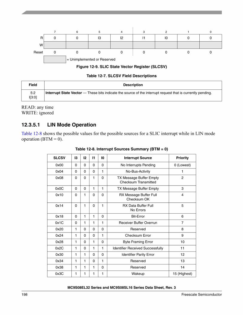
MC9S08EL32 Series and MC9S08SL16 Series Data Sheet, Rev. 3
198 Freescale Semiconductor
READ: any timeWRITE: ignored
12.3.5.1 LIN Mode Operation
Table 12-8 shows the possible values for the possible sources for a SLIC interrupt while in LIN mode operation (BTM = 0).
7 6 5 4 3 2 1 0
R 0 0 I3 I2 I1 I0 0 0
W
Reset 0 0 0 0 0 0 0 0
= Unimplemented or Reserved
Figure 12-9. SLIC State Vector Register (SLCSV)
Table 12-7. SLCSV Field Descriptions
Field Description
5:2I[3:0]
Interrupt State Vector — These bits indicate the source of the interrupt request that is currently pending.
Table 12-8. Interrupt Sources Summary (BTM = 0)
SLCSV I3 I2 I1 I0 Interrupt Source Priority
0x00 0 0 0 0 No Interrupts Pending 0 (Lowest)
0x04 0 0 0 1 No-Bus-Activity 1
0x08 0 0 1 0 TX Message Buffer EmptyChecksum Transmitted
2
0x0C 0 0 1 1 TX Message Buffer Empty 3
0x10 0 1 0 0 RX Message Buffer FullChecksum OK
4
0x14 0 1 0 1 RX Data Buffer FullNo Errors
5
0x18 0 1 1 0 Bit-Error 6
0x1C 0 1 1 1 Receiver Buffer Overrun 7
0x20 1 0 0 0 Reserved 8
0x24 1 0 0 1 Checksum Error 9
0x28 1 0 1 0 Byte Framing Error 10
0x2C 1 0 1 1 Identifier Received Successfully 11
0x30 1 1 0 0 Identifier Parity Error 12
0x34 1 1 0 1 Reserved 13
0x38 1 1 1 0 Reserved 14
0x3C 1 1 1 1 Wakeup 15 (Highest)
MC9S08EL32 Series and MC9S08SL16 Series Data Sheet, Rev. 3
Freescale Semiconductor 199
• No Interrupts PendingThis value indicates that all pending interrupt sources have been serviced. In polling mode, the SLCSV is read and interrupts serviced until this value reads back 0. This source will not generate an interrupt of the CPU, regardless of state of SLCIE.
• No Bus Activity (LIN specified error)The No-Bus-Activity condition occurs if no valid SYNCH BREAK FIELD or BYTE FIELD was received for more than 223 SLIC clock counts since the reception of the last valid message. For example, with 10 MHz SLIC clock frequency, a No-Bus-Activity interrupt will occur approximately 0.839 seconds after the bus begins to idle.
• TX Message Buffer Empty — Checksum TransmittedWhen the entire LIN message frame has been transmitted successfully, complete with the appropriately selected checksum byte, this interrupt source is asserted. This source is used for all standard LIN message frames and the final set of bytes with extended LIN message frames.
• TX Message Buffer EmptyThis interrupt source indicates that all 8 bytes in the LIN message buffer have been transmitted with no checksum appended. This source is used for intermediate sets of 8 bytes in extended LIN message frames.
• RX Message Buffer Full — Checksum OKWhen the entire LIN message frame has been received successfully, complete with the appropriately selected checksum byte, and the checksum calculates correctly, this interrupt source is asserted. This source is used for all standard LIN message frames and the final set of bytes with extended LIN message frames. To clear this source, SLCD0 must be read first.
• RX Data Buffer Full — No Errors This interrupt source indicates that 8 bytes have been received with no checksum byte and are waiting in the LIN message buffer. This source is used for intermediate sets of 8 bytes in extended LIN message frames. To clear this source, SLCD0 must be read first.
• Bit ErrorA unit that is sending a bit on the bus also monitors the bus. A BIT_ERROR must be detected at that bit time, when the bit value that is monitored is different from the bit value that is sent. The SLIC will terminate the data transmission upon detection of a bit error, according to the LIN specification. Bit errors are not checked when the LIN bus is running at high speed due to the effects of physical layer round trip delay. Bit errors are checked only when BEDD = 0.
• Receiver Buffer Overrun ErrorThis error is an indication that the receive buffer has not been emptied and additional bytes have been received, resulting in lost data. Because this interrupt is higher priority than the receive buffer full interrupts, it will appear first when an overflow condition occurs. There will, however, be a pending receive interrupt which must also be cleared after the buffer overrun flag is cleared. Buffer overrun errors can be avoided if on reception of data complete with checksum correct (SLCSV=$10) SLCD0 is read, the software sets IMSG after reception of a valid ID, the software enters BTM mode, or received data causes a framing or checksum error to occur.
• Checksum Error (LIN specified error)The checksum error occurs when the calculated checksum value does not match the expected value. If this error is encountered, it is important to verify that the correct checksum calculation
MC9S08EL32 Series and MC9S08SL16 Series Data Sheet, Rev. 3
200 Freescale Semiconductor
method was employed for this message frame. Refer to the LIN specification for more details on the calculations.
• Byte Framing ErrorThis error comes from the standard UART definition for byte encoding and occurs when the STOP bit is sampled and reads back as a 090. STOP should always read as 1.
NOTEA byte framing error can also be an indication that the number of data bytes received in a LIN message frame does not match the value written to the SLCDLC register. See Section 12.6.7, “Handling LIN Message Headers,” for more details.
• Identifier Received SuccessfullyThis interrupt source indicates that a LIN identifier byte has been received with correct parity and is waiting in the LIN identifier buffer (SLCID). Upon reading this interrupt source from SLCSV, the user can then decode the identifier in software to determine the nature of the LIN message frame. To clear this source, SLCID must be read.
• Identifier-Parity-Error A parity error in the identifier (i.e., corrupted identifier) will be flagged. Typical LIN slave applications do not distinguish between an unknown but valid identifier, and a corrupted identifier. However, it is mandatory for all slave nodes to evaluate in case of a known identifier all eight bits of the ID-Field and distinguish between a known and a corrupted identifier. The received identifier value is reported in SLCID so that the user software can choose to acknowledge or ignore the parity error message. Once the ID parity error has been detected, the SLIC will begin looking for another LIN header and will not receive message data, even if it appears on the bus.
• WakeupThe wakeup interrupt source indicates that the SLIC module has entered SLIC run mode from SLIC stop mode.
12.3.5.2 Byte Transfer Mode Operation
When byte transfer mode is enabled (BTM = 1), many of the interrupt sources for the SLCSV no longer apply, as they are specific to LIN operations. Table 12-9 shows those interrupt sources which are applicable to BTM operations. The value of the SLCSV for each interrupt source remains the same, as well as the priority of the interrupt source.
I
Table 12-9. Interrupt Sources Summary (BTM = 1)
SLCSV I3 I2 I1 I0 Interrupt Source Priority
0x00 0 0 0 0 No Interrupts Pending 0 (Lowest)
0x0C 0 0 1 1 TX Message Buffer Empty 3
0x14 0 1 0 1 RX Data Buffer FullNo Errors
5
0x18 0 1 1 0 Bit-Error 6
0x1C 0 1 1 1 Receiver Buffer Overrun 7
MC9S08EL32 Series and MC9S08SL16 Series Data Sheet, Rev. 3
Freescale Semiconductor 201
• No Interrupts PendingThis value indicates that all pending interrupt sources have been serviced. In polling mode, the SLCSV is read and interrupts serviced until this value reads back 0. This source will not generate an interrupt of the CPU, regardless of state of SLCIE.
• TX Message Buffer EmptyIn byte transfer mode, this interrupt source indicates that the byte in the SLCID has been transmitted.
• RX Data Buffer Full — No ErrorsThis interrupt source indicates that a byte has been received and is waiting in SLCID. To clear this source, SLCID must be read first.
• Bit ErrorA unit that is sending a bit on the bus also monitors the bus. A BIT_ERROR must be detected at that bit time, when the bit value that is monitored is different from the bit value that is sent. The SLIC will terminate the data transmission upon detection of a bit error, according to the LIN specification. Bit errors are not checked when the LIN bus is running at high speed due to the effects of physical layer round trip delay. Bit errors are checked only when BEDD = 0.
• Receiver Buffer Overrun ErrorThis error is an indication that the receive buffer has not been emptied and additional byte(s) have been received, resulting in lost data. Because this interrupt is higher priority than the receive buffer full interrupts, it will appear first when an overflow condition occurs. There will, however, be a pending receive interrupt which must also be cleared after the buffer overrun flag is cleared. Buffer overrun errors can be avoided if on reception of data (SLCSV=$14) SLCD0 is read or received data causes a framing error to occur.
• Byte Framing ErrorThis error comes from the standard UART definition for byte encoding and occurs when STOP is sampled and reads back as a 0. STOP should always read as 1. A byte framing error could be encountered if the bit timing value programmed in BTH:L does not match the bit rate of the incoming data.
•• Wakeup
The wakeup interrupt source indicates that the SLIC module has entered SLIC run mode from SLIC wait mode.
0x28 1 0 1 0 Byte Framing Error 10
0x38 1 1 1 0 Reserved 14
0x3C 1 1 1 1 Wakeup 15 (Highest)
Table 12-9. Interrupt Sources Summary (BTM = 1)
SLCSV I3 I2 I1 I0 Interrupt Source Priority
MC9S08EL32 Series and MC9S08SL16 Series Data Sheet, Rev. 3
202 Freescale Semiconductor
12.3.6 SLIC Data Length Code Register (SLCDLC)
The SLIC data length code register (SLCDLC) is the primary functional control register for the SLIC module during normal LIN operations. It contains the data length code of the message buffer, indicating how many bytes of data are to be sent or received, as well as the checksum mode control and transmit enabling bit.
7 6 5 4 3 2 1 0
RTXGO CHKMOD DLC5 DLC4 DLC3 DLC2 DLC1 DLC0
W
Reset 0 0 0 0 0 0 0 0
Figure 12-10. SLIC Data Length Code Register (SLCDLC)
Table 12-10. SLCDLC Field Descriptions
Field Description
7TXGO
SLIC Transmit Go — This bit controls whether the SLIC module is sending or receiving data bytes. This bit is automatically reset to 0 after a transmit operation is complete or an error is encountered and transmission has been aborted.0 SLIC receive data 1 Initiate SLIC transmit— The SLIC assumes the user has loaded the proper data into the message buffer and
will begin transmitting the number of bytes indicated in the SLCDLC bits. If the number of bytes is greater than 8, the first 8 bytes will be transmitted and an interrupt will be triggered (if unmasked) for the user to enter the next bytes of the message. If the number of bytes is 8 or fewer, the SLIC will transmit the appropriate number of bytes and automatically append the checksum to the transmission. If IMSG or TXABRT are set or the SLCF flag is set, writes to TXGO will have no effect.
6CHKMOD
LIN Checksum Mode — CHKMOD is used to decide what checksum method to use for this message frame. Resets after error code or message frame complete. CHKMOD must be written (124 desired) only after the reception of an identifier and before the reception or transmission of data bytes. Writing this bit to a one clears the current checksum calculation. 0 Checksum calculated 119 the identifier byte included
(SAE J2602/LIN 2.0)1 Checksum calculated without the identifier byte (LIN spec <= 1.3)
5:0DLC
Data Length Control Bits — The value of the bits indicate the number of data bytes in message. Values 0x00–0x07 are for “normal” LIN messaging. Values 0x08–0x3F are for “extended” LIN messaging. See Table 12-11.
Table 12-11. Data Length Control
DLC[5:0] Message Data Length (Number of Bytes)
0x00 1
0x01 2
0x02 3
... ...
0x3D 62
0x3E 63
0x3F 64
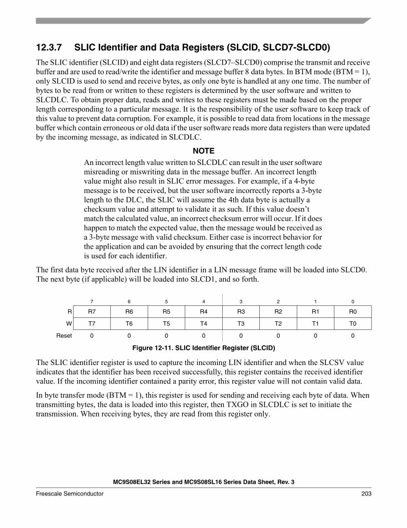
MC9S08EL32 Series and MC9S08SL16 Series Data Sheet, Rev. 3
Freescale Semiconductor 203
12.3.7 SLIC Identifier and Data Registers (SLCID, SLCD7-SLCD0)
The SLIC identifier (SLCID) and eight data registers (SLCD7–SLCD0) comprise the transmit and receive buffer and are used to read/write the identifier and message buffer 8 data bytes. In BTM mode (BTM = 1), only SLCID is used to send and receive bytes, as only one byte is handled at any one time. The number of bytes to be read from or written to these registers is determined by the user software and written to SLCDLC. To obtain proper data, reads and writes to these registers must be made based on the proper length corresponding to a particular message. It is the responsibility of the user software to keep track of this value to prevent data corruption. For example, it is possible to read data from locations in the message buffer which contain erroneous or old data if the user software reads more data registers than were updated by the incoming message, as indicated in SLCDLC.
NOTEAn incorrect length value written to SLCDLC can result in the user software misreading or miswriting data in the message buffer. An incorrect length value might also result in SLIC error messages. For example, if a 4-byte message is to be received, but the user software incorrectly reports a 3-byte length to the DLC, the SLIC will assume the 4th data byte is actually a checksum value and attempt to validate it as such. If this value doesn’t match the calculated value, an incorrect checksum error will occur. If it does happen to match the expected value, then the message would be received as a 3-byte message with valid checksum. Either case is incorrect behavior for the application and can be avoided by ensuring that the correct length code is used for each identifier.
The first data byte received after the LIN identifier in a LIN message frame will be loaded into SLCD0. The next byte (if applicable) will be loaded into SLCD1, and so forth.
The SLIC identifier register is used to capture the incoming LIN identifier and when the SLCSV value indicates that the identifier has been received successfully, this register contains the received identifier value. If the incoming identifier contained a parity error, this register value will not contain valid data.
In byte transfer mode (BTM = 1), this register is used for sending and receiving each byte of data. When transmitting bytes, the data is loaded into this register, then TXGO in SLCDLC is set to initiate the transmission. When receiving bytes, they are read from this register only.
7 6 5 4 3 2 1 0
R R7 R6 R5 R4 R3 R2 R1 R0
W T7 T6 T5 T4 T3 T2 T1 T0
Reset 0 0 0 0 0 0 0 0
Figure 12-11. SLIC Identifier Register (SLCID)
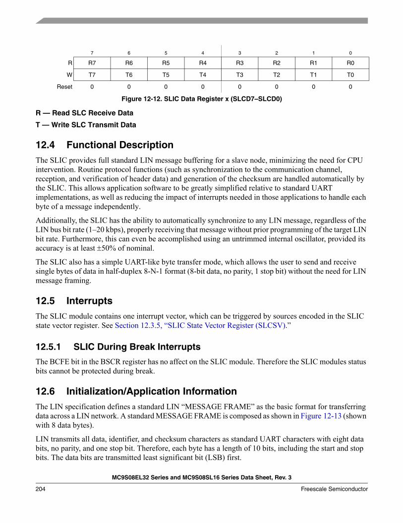
MC9S08EL32 Series and MC9S08SL16 Series Data Sheet, Rev. 3
204 Freescale Semiconductor
R — Read SLC Receive Data
T — Write SLC Transmit Data
12.4 Functional DescriptionThe SLIC provides full standard LIN message buffering for a slave node, minimizing the need for CPU intervention. Routine protocol functions (such as synchronization to the communication channel, reception, and verification of header data) and generation of the checksum are handled automatically by the SLIC. This allows application software to be greatly simplified relative to standard UART implementations, as well as reducing the impact of interrupts needed in those applications to handle each byte of a message independently.
Additionally, the SLIC has the ability to automatically synchronize to any LIN message, regardless of the LIN bus bit rate (1–20 kbps), properly receiving that message without prior programming of the target LIN bit rate. Furthermore, this can even be accomplished using an untrimmed internal oscillator, provided its accuracy is at least ±50% of nominal.
The SLIC also has a simple UART-like byte transfer mode, which allows the user to send and receive single bytes of data in half-duplex 8-N-1 format (8-bit data, no parity, 1 stop bit) without the need for LIN message framing.
12.5 Interrupts The SLIC module contains one interrupt vector, which can be triggered by sources encoded in the SLIC state vector register. See Section 12.3.5, “SLIC State Vector Register (SLCSV).”
12.5.1 SLIC During Break Interrupts
The BCFE bit in the BSCR register has no affect on the SLIC module. Therefore the SLIC modules status bits cannot be protected during break.
12.6 Initialization/Application InformationThe LIN specification defines a standard LIN “MESSAGE FRAME” as the basic format for transferring data across a LIN network. A standard MESSAGE FRAME is composed as shown in Figure 12-13 (shown with 8 data bytes).
LIN transmits all data, identifier, and checksum characters as standard UART characters with eight data bits, no parity, and one stop bit. Therefore, each byte has a length of 10 bits, including the start and stop bits. The data bits are transmitted least significant bit (LSB) first.
7 6 5 4 3 2 1 0
R R7 R6 R5 R4 R3 R2 R1 R0
W T7 T6 T5 T4 T3 T2 T1 T0
Reset 0 0 0 0 0 0 0 0
Figure 12-12. SLIC Data Register x (SLCD7–SLCD0)
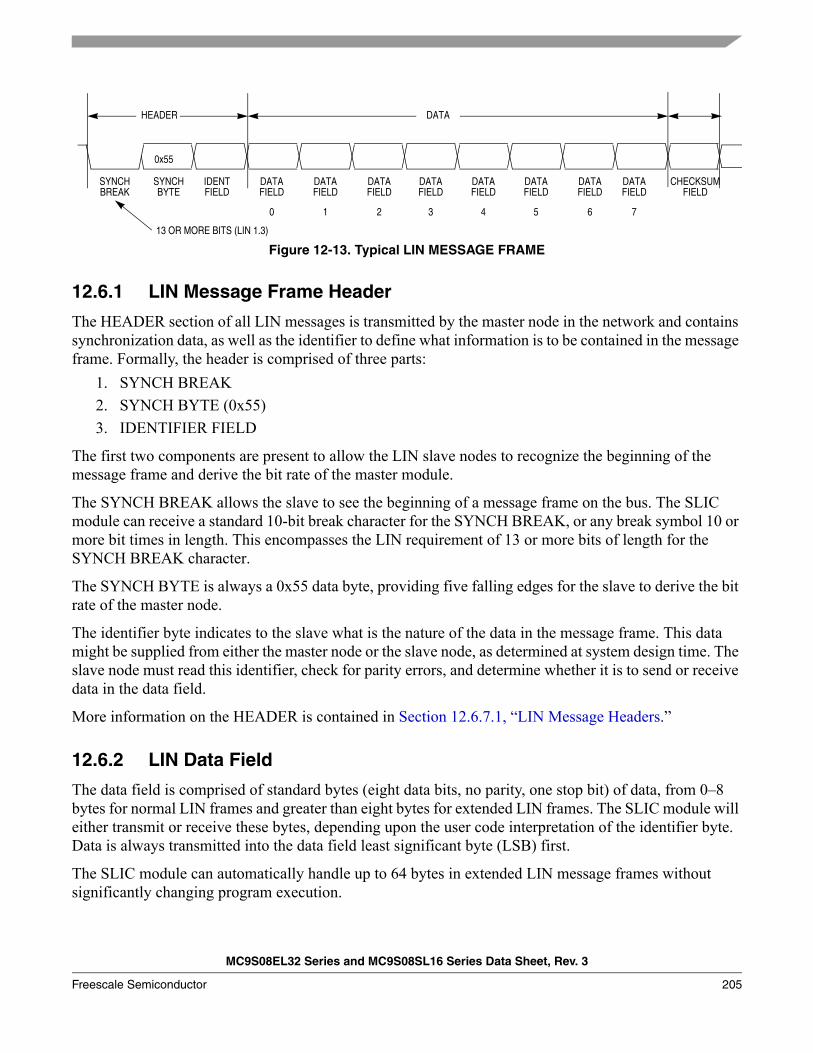
MC9S08EL32 Series and MC9S08SL16 Series Data Sheet, Rev. 3
Freescale Semiconductor 205
Figure 12-13. Typical LIN MESSAGE FRAME
12.6.1 LIN Message Frame Header
The HEADER section of all LIN messages is transmitted by the master node in the network and contains synchronization data, as well as the identifier to define what information is to be contained in the message frame. Formally, the header is comprised of three parts:
1. SYNCH BREAK2. SYNCH BYTE (0x55)3. IDENTIFIER FIELD
The first two components are present to allow the LIN slave nodes to recognize the beginning of the message frame and derive the bit rate of the master module.
The SYNCH BREAK allows the slave to see the beginning of a message frame on the bus. The SLIC module can receive a standard 10-bit break character for the SYNCH BREAK, or any break symbol 10 or more bit times in length. This encompasses the LIN requirement of 13 or more bits of length for the SYNCH BREAK character.
The SYNCH BYTE is always a 0x55 data byte, providing five falling edges for the slave to derive the bit rate of the master node.
The identifier byte indicates to the slave what is the nature of the data in the message frame. This data might be supplied from either the master node or the slave node, as determined at system design time. The slave node must read this identifier, check for parity errors, and determine whether it is to send or receive data in the data field.
More information on the HEADER is contained in Section 12.6.7.1, “LIN Message Headers.”
12.6.2 LIN Data Field
The data field is comprised of standard bytes (eight data bits, no parity, one stop bit) of data, from 0–8 bytes for normal LIN frames and greater than eight bytes for extended LIN frames. The SLIC module will either transmit or receive these bytes, depending upon the user code interpretation of the identifier byte. Data is always transmitted into the data field least significant byte (LSB) first.
The SLIC module can automatically handle up to 64 bytes in extended LIN message frames without significantly changing program execution.
SYNCHBREAK
SYNCHBYTE
IDENTFIELD
DATAFIELD
DATAFIELD
DATAFIELD
DATAFIELD
DATAFIELD
DATAFIELD
DATAFIELD
CHECKSUMFIELD
DATAFIELD
0 1 2 3 4 5 6 7
0x55
13 OR MORE BITS (LIN 1.3)
HEADER DATA
MC9S08EL32 Series and MC9S08SL16 Series Data Sheet, Rev. 3
206 Freescale Semiconductor
12.6.3 LIN Checksum Field
The checksum field is a data integrity measure for LIN message frames, used to signal errors in data consistency. The LIN 1.3 checksum calculation only covers the data field, but the SLIC module also supports an enhanced checksum calculation which also includes the identifier field. For more information on the checksum calculation, refer to Section 12.6.13, “LIN Data Integrity Checking Methods.”
12.6.4 SLIC Module Constraints
In designing a practical module, certain reasonable constraints must be placed on the LIN message traffic which are not necessarily explicitly specified in the LIN specification. The SLIC module presumes that:
• Timeout for no-bus-activity = 1 second.
12.6.5 SLCSV Interrupt Handling
Each change of state of the SLIC module is encoded in the SLIC state vector register (SLCSV). This is an efficient method of handling state changes, indicating to the user not only the current status of the SLIC module, but each state change will also generate an interrupt (if SLIC interrupts are enabled). For more detailed information on the SLCSV, please refer to Section 12.3.5, “SLIC State Vector Register (SLCSV).”
In the software diagrams in the following subsections, when an interrupt is shown, the first step must always be reading SLCSV to determine what is the current status of the SLIC module. Likewise, when the diagrams indicate to “EXIT ISR”, the final step to exiting the interrupt service routine is to clear the SLCF interrupt flag. This can only be done if the SLCSV has first been read, and in the case that data has been received (such as an ID byte or command message data) the SLCD has been read at least one time.
After SLCSV is read, it will switch to the next pending state, so the user must be sure it is copied only once into a software variable at the beginning of the interrupt service routine to avoid inadvertently clearing a pending interrupt source. Additional decisions based on this value must be made from the software variable, rather than from the SLCSV itself.
After exiting the ISR, normal application code may resume. If the diagram indicates to “RETURN TO IDLE,” it indicates that all processing for the current message frame has been completed. If an error was detected and the corresponding error code loaded into the SLCSV, any pending data in the data buffer will be flushed out and the SLIC returned to its idle state, seeking out the next message frame header.
12.6.6 SLIC Module Initialization Procedure
12.6.6.1 LIN Mode Initialization
The SLIC module does not require very much initialization, due to its self-synchronizing design. Because no prior knowledge of the bit rate is required to synchronize to the LIN bus, no programming of bit rate is required.
At initialization time, the user must configure:• SLIC prescale register (SLIC digital receive filter adjustment).• Wait clock mode operation.
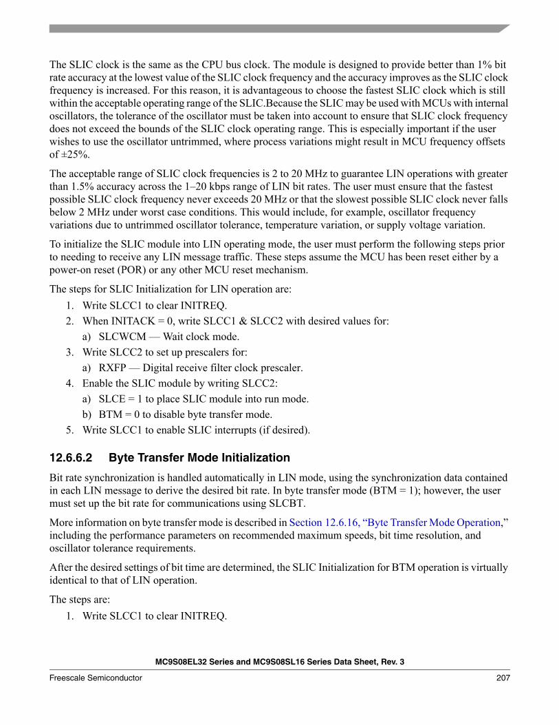
MC9S08EL32 Series and MC9S08SL16 Series Data Sheet, Rev. 3
Freescale Semiconductor 207
The SLIC clock is the same as the CPU bus clock. The module is designed to provide better than 1% bit rate accuracy at the lowest value of the SLIC clock frequency and the accuracy improves as the SLIC clock frequency is increased. For this reason, it is advantageous to choose the fastest SLIC clock which is still within the acceptable operating range of the SLIC.Because the SLIC may be used with MCUs with internal oscillators, the tolerance of the oscillator must be taken into account to ensure that SLIC clock frequency does not exceed the bounds of the SLIC clock operating range. This is especially important if the user wishes to use the oscillator untrimmed, where process variations might result in MCU frequency offsets of ±25%.
The acceptable range of SLIC clock frequencies is 2 to 20 MHz to guarantee LIN operations with greater than 1.5% accuracy across the 1–20 kbps range of LIN bit rates. The user must ensure that the fastest possible SLIC clock frequency never exceeds 20 MHz or that the slowest possible SLIC clock never falls below 2 MHz under worst case conditions. This would include, for example, oscillator frequency variations due to untrimmed oscillator tolerance, temperature variation, or supply voltage variation.
To initialize the SLIC module into LIN operating mode, the user must perform the following steps prior to needing to receive any LIN message traffic. These steps assume the MCU has been reset either by a power-on reset (POR) or any other MCU reset mechanism.
The steps for SLIC Initialization for LIN operation are:1. Write SLCC1 to clear INITREQ.2. When INITACK = 0, write SLCC1 & SLCC2 with desired values for:
a) SLCWCM — Wait clock mode.3. Write SLCC2 to set up prescalers for:
a) RXFP — Digital receive filter clock prescaler.4. Enable the SLIC module by writing SLCC2:
a) SLCE = 1 to place SLIC module into run mode.b) BTM = 0 to disable byte transfer mode.
5. Write SLCC1 to enable SLIC interrupts (if desired).
12.6.6.2 Byte Transfer Mode Initialization
Bit rate synchronization is handled automatically in LIN mode, using the synchronization data contained in each LIN message to derive the desired bit rate. In byte transfer mode (BTM = 1); however, the user must set up the bit rate for communications using SLCBT.
More information on byte transfer mode is described in Section 12.6.16, “Byte Transfer Mode Operation,” including the performance parameters on recommended maximum speeds, bit time resolution, and oscillator tolerance requirements.
After the desired settings of bit time are determined, the SLIC Initialization for BTM operation is virtually identical to that of LIN operation.
The steps are:1. Write SLCC1 to clear INITREQ.
MC9S08EL32 Series and MC9S08SL16 Series Data Sheet, Rev. 3
208 Freescale Semiconductor
2. When INITACK = 0, write SLCC2 with desired values for:a) SLCWCM — Wait clock mode.
3. Write SLCC2 to set up:a) RXFP — Digital receive filter clock prescaler.
4. Enable the SLIC module by writing SLCC2:a) SLCE = 1 to place SLIC module into run mode.b) BTM = 1 to enable byte transfer mode.
5. Write SLCBT value.6. Write SLCC1 to enable SLIC interrupts (if desired).
NOTEThe SLIC module is designed primarily for use in LIN systems and assumes the connection of a LIN transceiver, which provides a resistive path between the transmit and receive pins. BTM mode will not operate properly without a resistive feedback path between SLCTx and SLCRx.
12.6.7 Handling LIN Message Headers
Figure 12-14 shows how the SLIC module deals with incoming LIN message headers.
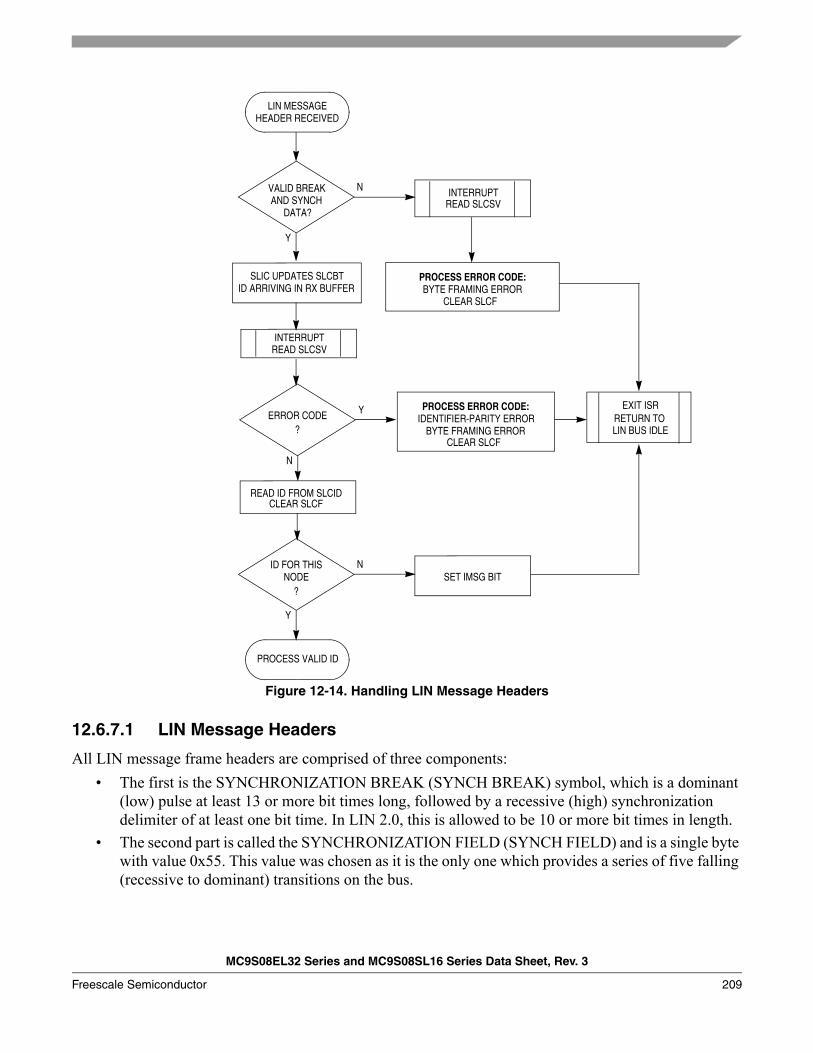
MC9S08EL32 Series and MC9S08SL16 Series Data Sheet, Rev. 3
Freescale Semiconductor 209
Figure 12-14. Handling LIN Message Headers
12.6.7.1 LIN Message Headers
All LIN message frame headers are comprised of three components:• The first is the SYNCHRONIZATION BREAK (SYNCH BREAK) symbol, which is a dominant
(low) pulse at least 13 or more bit times long, followed by a recessive (high) synchronization delimiter of at least one bit time. In LIN 2.0, this is allowed to be 10 or more bit times in length.
• The second part is called the SYNCHRONIZATION FIELD (SYNCH FIELD) and is a single byte with value 0x55. This value was chosen as it is the only one which provides a series of five falling (recessive to dominant) transitions on the bus.
PROCESS ERROR CODE:
LIN MESSAGEHEADER RECEIVED
SLIC UPDATES SLCBTID ARRIVING IN RX BUFFER
N
Y
ERROR CODE?
Y
N
ID FOR THIS
?
N
Y
NODE
INTERRUPT
PROCESS VALID ID
BYTE FRAMING ERROR
PROCESS ERROR CODE:IDENTIFIER-PARITY ERROR
SET IMSG BIT
BYTE FRAMING ERROR
EXIT ISRRETURN TO
READ ID FROM SLCID
READ SLCSV
LIN BUS IDLE
VALID BREAKAND SYNCH
DATA?
INTERRUPTREAD SLCSV
CLEAR SLCF
CLEAR SLCF
CLEAR SLCF
MC9S08EL32 Series and MC9S08SL16 Series Data Sheet, Rev. 3
210 Freescale Semiconductor
• The third section of the message frame header is the IDENTIFIER FIELD (ID). The identifier is covered more in Section 12.6.8, “Handling Command Message Frames,” and Section 12.6.9, “Handling Request LIN Message Frames.”
The SLIC automatically reads the incoming pattern of the SYNCHRONIZATION BREAK and FIELD and determines the bit rate of the LIN data frame, as well as checking for errors in form and discerning between a genuine BREAK/FIELD combination and a similar byte pattern somewhere in the data stream. After the header has been verified to be valid and has been processed, the SLIC module updates the SLIC bit time register (SLCBT) with the value obtained from the SYNCH FIELD and begins to receive the ID.
After the ID for the message frame has been received, an interrupt is generated by the SLIC and will trigger an MCU interrupt request if unmasked. At this point, it might be possible that the ID was received with errors such as a parity error (based on the LIN specification) or a byte framing error. If the ID did not have any errors, it will be copied into the SLCD for the software to read. The SLCSV will indicate the type error or that the ID was received correctly.
In a LIN system, the meaning and function of all messages, and therefore all message identifiers, is pre-defined by the system designer. This information can be collected and stored in a standardized format file, called a Configuration Language Description (CLD) file. In using the SLIC module, it is the responsibility of the user software to determine the nature of the incoming message, and therefore how to further handle that message.
The simplest case is when the SLIC receives a message which the user software determines is of no interest to the application. In other words, the slave node does not need to receive or transmit any data for this message frame. This might also apply to messages with zero data bytes (which is allowed by the LIN specification). At this point, the user can set the IMSG control bit, and exit the interrupt service routine by clearing the SLCIF flag. Because there is no data to be sent or received, the SLIC will not generate another interrupt until the next message frame header or bus goes idle long enough to trigger a “No-Bus-Activity” error according to the LIN specification.
NOTEIMSG will prevent another interrupt from occurring for the current message frame; however, if data bytes are appearing on the bus they may be received and copied into the message buffer. This will delete any previous data which might have been present in the buffer, even though no interrupt is triggered to indicate the arrival of this data.
At the time the ID is read, the user might also choose to read SLCBT and copy this value out to an application variable. This data can then be used at a time appropriate to both the application software and the LIN communications to adjust the trim of the internal oscillator. This operation must be handled very carefully to avoid adjusting the base timing of the MCU at the wrong time, adversely affecting the operation of the SLIC module or of the application itself. More information about this is contained in Section 12.6.17, “Oscillator Trimming with SLIC.”
If the user software determines that the ID read out of the SLCD corresponds to a command or request message for which this node needs to receive or transmit data (respectively), it will then move on to procedures described in Section 12.6.8, “Handling Command Message Frames,” and Section 12.6.9, “Handling Request LIN Message Frames.”
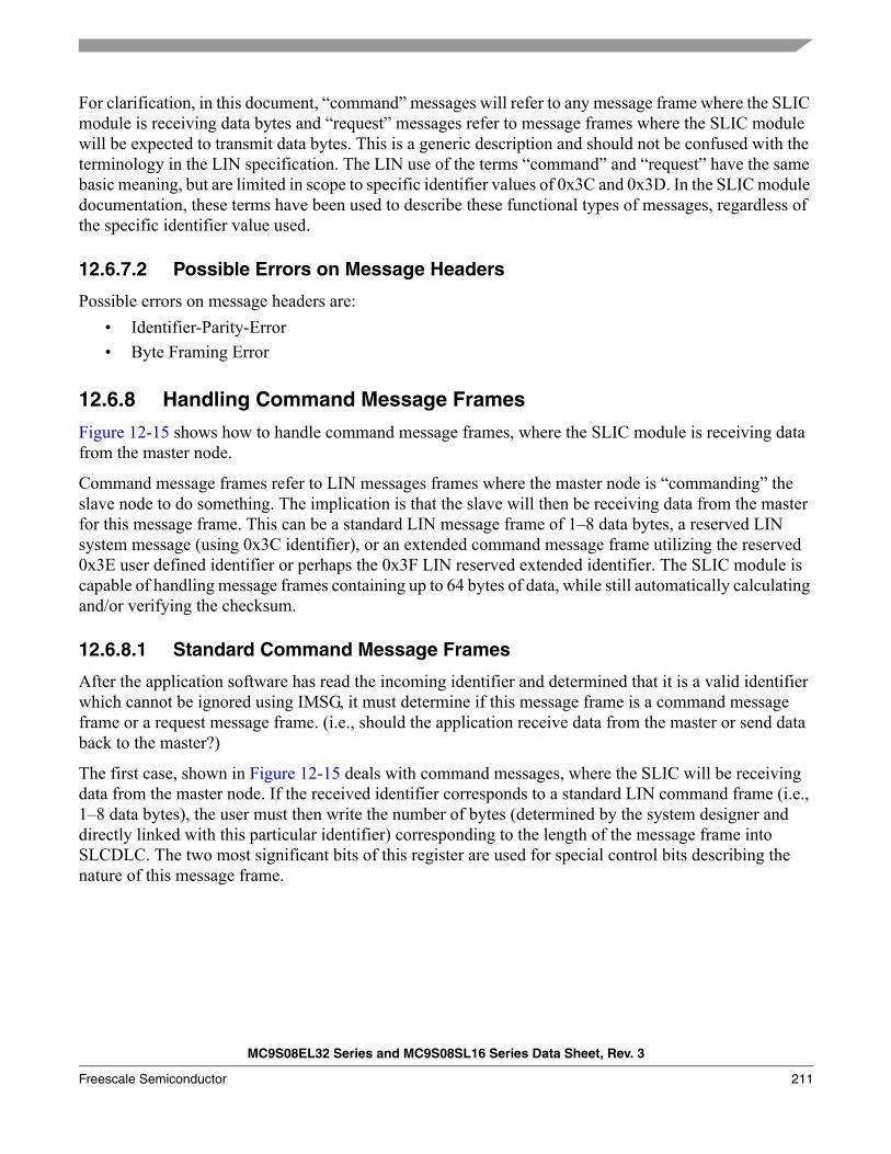
MC9S08EL32 Series and MC9S08SL16 Series Data Sheet, Rev. 3
Freescale Semiconductor 211
For clarification, in this document, “command” messages will refer to any message frame where the SLIC module is receiving data bytes and “request” messages refer to message frames where the SLIC module will be expected to transmit data bytes. This is a generic description and should not be confused with the terminology in the LIN specification. The LIN use of the terms “command” and “request” have the same basic meaning, but are limited in scope to specific identifier values of 0x3C and 0x3D. In the SLIC module documentation, these terms have been used to describe these functional types of messages, regardless of the specific identifier value used.
12.6.7.2 Possible Errors on Message Headers
Possible errors on message headers are:• Identifier-Parity-Error• Byte Framing Error
12.6.8 Handling Command Message Frames
Figure 12-15 shows how to handle command message frames, where the SLIC module is receiving data from the master node.
Command message frames refer to LIN messages frames where the master node is “commanding” the slave node to do something. The implication is that the slave will then be receiving data from the master for this message frame. This can be a standard LIN message frame of 1–8 data bytes, a reserved LIN system message (using 0x3C identifier), or an extended command message frame utilizing the reserved 0x3E user defined identifier or perhaps the 0x3F LIN reserved extended identifier. The SLIC module is capable of handling message frames containing up to 64 bytes of data, while still automatically calculating and/or verifying the checksum.
12.6.8.1 Standard Command Message Frames
After the application software has read the incoming identifier and determined that it is a valid identifier which cannot be ignored using IMSG, it must determine if this message frame is a command message frame or a request message frame. (i.e., should the application receive data from the master or send data back to the master?)
The first case, shown in Figure 12-15 deals with command messages, where the SLIC will be receiving data from the master node. If the received identifier corresponds to a standard LIN command frame (i.e., 1–8 data bytes), the user must then write the number of bytes (determined by the system designer and directly linked with this particular identifier) corresponding to the length of the message frame into SLCDLC. The two most significant bits of this register are used for special control bits describing the nature of this message frame.
MC9S08EL32 Series and MC9S08SL16 Series Data Sheet, Rev. 3
212 Freescale Semiconductor
Figure 12-15. Handling Command Messages (Data Receive)
The SLIC transmit go (TXGO) bit should be 0 for command frames, indicating to the SLIC that data is coming from the master. The checksum mode control (CHKMOD) bit allows the user to select which method of checksum calculation is desired for this message frame. The LIN 1.3 checksum does not include the identifier byte in the calculation, while the SAE version does include this byte. Because the identifier is already received by the SLIC by this time, the default is to include it in the calculation. If a LIN 1.3 checksum is desired, a 1 in CHKMOD will reset the checksum circuitry to begin calculating the checksum
COMMAND MESSAGE?
PROCESSVALID ID
N
Y
INITIALIZE SW BYTE COUNT
PROCESSREQUEST MESSAGE
EXTENDED FRAME
?
Y
N
WRITE SLCDLC FOR THIS ID0nxx xxxx(TXGO = 0)(CHKMOD = n)
EXIT ISR
ERROR CODE
?
Y
N
PROCESS ERROR CODE:
EXIT ISRRETURN TO IDLE1. EMPTY RX BUFFER
2. DECREMENT SW BYTE COUNT BY 8
LAST FRAME
?
Y
N(SW BYTE COUNT <8)
WRITE SLCDLC FOR THIS ID0n00 0xxx(TXGO = 0)(CHKMOD = n)
EXIT ISR
ERROR CODE
?
Y
N
PROCESS ERROR CODE:
EXIT ISRRETURN TO IDLE EMPTY RX BUFFER
BYTE FRAMING ERRORCHECKSUM-ERRORNO-BUS-ACTIVITY
BYTE FRAMING ERRORNO-BUS-ACTIVITY
INTERRUPTREAD SLCSV
INTERRUPTREAD SLCSV
RECEIVE BUFFER OVERRUN
RECEIVE BUFFER OVERRUN
CLEAR SLCF
3. CLEAR SLCF
CLEAR SLCF
CLEAR SLCF
MC9S08EL32 Series and MC9S08SL16 Series Data Sheet, Rev. 3
Freescale Semiconductor 213
on the first data byte. Using CHKMOD in this way allows the SLIC to receive messages with either method of data consistency check and change on a frame-by-frame basis. If a system uses both types of data consistency checking methods, the software must simply change the setting of this bit based on the identifier of each message. If the network only uses one type of check, CHKMOD can be set as a constant value in the user’s code. If CHKMOD is not written on each frame, care must be taken not to accidentally modify the bit when writing the data length and TXGO bits. This is especially true if using C code without carefully inspecting the output of the compiler and assembler.
The control bits and data length code are contained in one register, allowing the user to maximize the efficiency of the identifier processing by writing a single byte value to indicate the nature of the message frame. This allows very efficient identifier processing code, which is important in a command frame, as the master node can be sending data immediately following the identifier byte which might be as little as one byte in length. The SLIC module uses a separate internal storage area for the incoming data bytes, so there is no danger of losing incoming data, but the user should spend as little time as possible within the ISR to ensure that the application or other ISRs are able to use the majority of the CPU bandwidth.
The identifier must be processed in a maximum of 2 byte times on the LIN bus to ensure that the ISR completes before the checksum would be received for the shortest possible message. This should be easily achievable, as the only operations required are to read SLCID and look up the checksum method, data length, and command/request state of that identifier, then write that value to the SLCDLC. This can be easily streamlined in code with a lookup table of identifiers and corresponding SLCDLC bytes.
NOTEOnce the ID is decoded for a message header and a length code written to SLCDLC, the SLIC is expecting that number of bytes to be received. If the SLIC module doesn't receive the number of bytes indicated in the SLCDLC register, it will continue to look for data bytes. If another message header begins, a byte framing error will trigger on the break symbol of that second message. The second message will still properly generate an ID received interrupt, but the byte framing error prior to this is an indication to the application that the previous message was not properly handled and should be discarded.
12.6.8.2 Extended Command Message Frames
Handling of extended frames is very similar to handling of standard frames, providing that the length is less than or equal to 64 bytes. Because the SLIC module can only receive 8 bytes at a time, the receive buffer must be emptied periodically for long message frames. This is not standard LIN operation, and is likely only to be used for downloading calibration data or reprogramming FLASH devices in a factory or service facility, so the added steps required for processing are not as critical to performance. During these types of operations, the application code is likely very limited in scope and special adjustments can be made to compensate for added message processing time.
For extended command frames, the data length is still written one time at the time the identifier is decoded, along with the TXGO and CHKMOD bits. When this is done, a software counter must also be initialized to keep track of how many bytes are expected to be received in the message frame. The ISR completes, clearing the SLCF flag, and resumes application execution. The SLIC will generate an interrupt, if
MC9S08EL32 Series and MC9S08SL16 Series Data Sheet, Rev. 3
214 Freescale Semiconductor
unmasked, after 8 bytes are received or an error is detected. At this interrupt, the SLCSV will indicate an error condition (in case of byte framing error, idle bus) or that the receive buffer is full. If the data is successfully received, the user must then empty the buffer by reading SLCD7-SLCD0 and then subtract 8 from the software byte count. When this software counter reaches 8 or fewer, the remaining data bytes will fit in the buffer and only one interrupt should occur. At this time, the final interrupt may be handled normally, continuing to use the software counter to read the proper number of bytes from the appropriate SLCD registers.
NOTE Do not write SLCDLC more than one time per LIN message frame. The SLIC tracks the number of sent or received bytes based on the value written to this register at the beginning of the data field and rewriting this register will corrupt the checksum calculation and cause unpredictable behavior in the SLIC module. The application software must track the number of sent or received bytes to know what the current byte count in the SLIC is. If programming in C, make sure to use the VOLATILE modifier on this variable (or make it a global variable) to ensure that it keeps its value between interrupts.
12.6.8.3 Possible Errors on Command Message Data
Possible errors on command message data are:• Byte Framing Error• Checksum-Error (LIN specified error)• No-Bus-Activity (LIN specified error)• Receiver Buffer Overrun Error
12.6.9 Handling Request LIN Message Frames
Figure 12-16 shows how to handle request message frames, where the SLIC module is sending data to the master node.
Request message frames refer to LIN messages frames where the master node is “requesting” the slave node to supply information. The implication is that the slave will then be transmitting data to the master for this message frame. This can be a standard LIN message frame of 1–8 data bytes, a reserved LIN system message (using 0x3D identifier), or an extended request message frame utilizing the reserved 0x3E identifier or perhaps the 0x3F LIN reserved extended identifier. The SLIC module is capable of handling request message frames containing up to 64 bytes of data, while still automatically calculating and/or verifying the checksum.
12.6.9.1 Standard Request Message Frames
Dealing with request messages with the SLIC is very similar to dealing with command messages, with one important difference. Because the SLIC is now to be transmitting data in the LIN message frame, the user software must load the data to be transmitted into the message buffer prior to initiating the transmission.
MC9S08EL32 Series and MC9S08SL16 Series Data Sheet, Rev. 3
Freescale Semiconductor 215
This means an extra step is taken inside the interrupt service routine after the identifier has been decoded and is determined to be an ID for a request message frame.
Figure 12-16 deals with request messages, where the SLIC will be transmitting data to the master node. If the received identifier corresponds to a standard LIN command frame (i.e., 1-8 data bytes), the message processing is very simple. The user must load the data to be transmitted into the transmit buffer by writing it to the SLCD registers. The first byte to be transmitted on the LIN bus must be loaded into SLCD0, then SLCD1 for the second byte, etc. After all of the bytes to be transmitted are loaded in this way, a single write to SLCDLC will allow the user to encode the number of data bytes to be transmitted (1–8 bytes for standard request frames), set the proper checksum calculation method for the data (CHKMOD), as well as signal the SLIC that the buffer is ready by writing a 1 to TXGO. TXGO will remain set to 1 until the buffer is sent successfully or an error is encountered, signaling to the application code that the buffer is in process of transmitting. In cases of 1–8 data bytes only being sent (standard LIN request frames), the SLIC automatically calculates and transmits the checksum byte at the end of the message frame. The user can exit the ISR after SLCDLC has been written and the SLCF flag has been cleared.
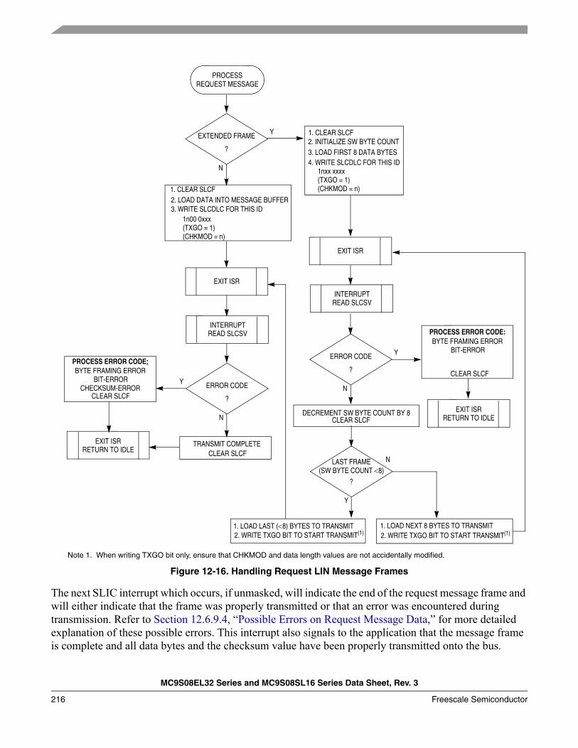
MC9S08EL32 Series and MC9S08SL16 Series Data Sheet, Rev. 3
216 Freescale Semiconductor
Figure 12-16. Handling Request LIN Message Frames
The next SLIC interrupt which occurs, if unmasked, will indicate the end of the request message frame and will either indicate that the frame was properly transmitted or that an error was encountered during transmission. Refer to Section 12.6.9.4, “Possible Errors on Request Message Data,” for more detailed explanation of these possible errors. This interrupt also signals to the application that the message frame is complete and all data bytes and the checksum value have been properly transmitted onto the bus.
PROCESSREQUEST MESSAGE
EXTENDED FRAME
?
Y
N4. WRITE SLCDLC FOR THIS ID
1nxx xxxx(TXGO = 1)(CHKMOD = n)
EXIT ISR
ERROR CODE
?
Y
N
PROCESS ERROR CODE:
EXIT ISRRETURN TO IDLE
DECREMENT SW BYTE COUNT BY 8
LAST FRAME
?
Y
N
(SW BYTE COUNT <8)
3. WRITE SLCDLC FOR THIS ID1n00 0xxx(TXGO = 1)(CHKMOD = n)
EXIT ISR
ERROR CODE
?
Y
N
PROCESS ERROR CODE:
EXIT ISRRETURN TO IDLE
TRANSMIT COMPLETE
2. INITIALIZE SW BYTE COUNT3. LOAD FIRST 8 DATA BYTES
2. LOAD DATA INTO MESSAGE BUFFER
1. LOAD LAST (<8) BYTES TO TRANSMIT
BYTE FRAMING ERRORBIT-ERROR
CHECKSUM-ERROR
BYTE FRAMING ERRORBIT-ERROR
INTERRUPTREAD SLCSV
INTERRUPTREAD SLCSV
2. WRITE TXGO BIT TO START TRANSMIT(1)1. LOAD NEXT 8 BYTES TO TRANSMIT2. WRITE TXGO BIT TO START TRANSMIT(1)
Note 1. When writing TXGO bit only, ensure that CHKMOD and data length values are not accidentally modified.
1. CLEAR SLCF
1. CLEAR SLCF
CLEAR SLCF
CLEAR SLCF
CLEAR SLCF
CLEAR SLCF
MC9S08EL32 Series and MC9S08SL16 Series Data Sheet, Rev. 3
Freescale Semiconductor 217
The SLIC module cannot begin to transmit the data until the user writes a 1 to TXGO, indicating that data is ready. If the user writes TXGO without loading data into the transmit buffer, whatever data is in storage will be transmitted, where the number of bytes transmitted is based on the data length value in the data length register. Similarly, if the user writes the wrong value for the number of data bytes to transmit, the SLIC will transmit that number of bytes, potentially transmitting garbage data onto the bus. The checksum calculation is performed based on the data transmitted, and will therefore still be calculated.
The identifier must be processed, data must be loaded into the transmit buffer, and the SLCDLC value written to initiate data transmission in a certain amount of time, based on the LIN specification. If the user waits too long to start transmission, the master node will observe an idle bus and trigger a Slave Not Responding error condition. The same error can be triggered if the transmission begins too late and does not complete before the message frame times out. Refer to the LIN specification for more details on timing constraints and requirements for LIN slave devices. This is especially important when dealing with extended request frames, when the data must be loaded in 8 byte sections (maximum) to be transmitted at each interrupt.
12.6.9.2 Extended Request Message Frames
Handling of extended frames is very similar to handling of standard frames, providing that the length is less than or equal to 64 bytes. Because the SLIC module can only transmit 8 bytes at a time, the transmit buffer must be loaded periodically for extended message frames. This is not standard LIN operation, and is likely only to be used for special cases, so the added steps required for processing should not be as critical to performance. During these types of operations, the application code is likely very limited in scope and special adjustments can be made to compensate for added message processing time.
When handling extended request frames, it is important to clear the SLCF flag first, before loading any data or writing TXGO. The data length is still written only one time, at the time the identifier is decoded, along with the TXGO and CHKMOD bits, after the first 8 data bytes are loaded into the transmit buffer. When this is done, a software counter must also be initialized to keep track of how many bytes are to be transmitted in the message frame. The SLIC will generate an interrupt, if unmasked, after 8 bytes are transmitted or an error is detected. At this interrupt, the SLCSV will indicate an error condition (in case of byte framing error or bit error) or that the transmit buffer is empty. If the data is transmitted successfully, the user must then clear the SLCF flag, subtract 8 from the software byte count, load the next 8 bytes into the SLCD registers, and write a 1 to TXGO to tell the SLIC that the buffers are loaded and transmission can commence. When this software counter reaches 8 or fewer, the remaining data bytes will fit in the transmit buffer and the SLIC will automatically append the checksum value to the frame after the last byte is sent.
MC9S08EL32 Series and MC9S08SL16 Series Data Sheet, Rev. 3
218 Freescale Semiconductor
NOTE Do not write the CHKMOD or data length values in SLCDLC more than one time per message frame. The SLIC tracks the number of sent or received bytes based on the value written to this register at the beginning of the data field and rewriting this register will corrupt the checksum calculation and cause unpredictable behavior in the SLIC module. The application software must track the number of sent or received bytes to know what the current byte count in the SLIC is. If programming in C, make sure to use the STATIC modifier on this variable (or make it a global variable) to ensure that it keeps its value between interrupts.
12.6.9.3 Transmit Abort
The transmit abort bit (TXABRT) in SLCC1 allows the user to cease transmission of data on the next byte boundary. When this bit is set to 1, it will finish transmitting the byte currently being transmitted, then cease transmission. After the transmission is successfully aborted, TXABRT will automatically be reset by the SLIC to 0. If the SLIC is not in process of transmitting at the time TXABRT is written to 1, there is no effect and TXABRT will read back as 0.
12.6.9.4 Possible Errors on Request Message Data
Possible errors on request message data are:• Byte Framing Error• Checksum-Error (LIN specified error)• Bit-Error
12.6.10 Handling IMSG to Minimize Interrupts
The IMSG feature is designed to minimize the number of interrupts required to maintain LIN communications. On a network with many slave nodes, it is very likely that a particular slave will observe messages which are not intended for that node. When the SLIC module detects any message header, it synchronizes to that message frame and bit rate, then interrupts the CPU after the identifier byte has been successfully received and parity checked. At this time, if the software determines that the message may be ignored, IMSG may be set to indicate to the module that the data field of the message frame is to be ignored and no additional interrupts should be generated until the next valid message header is received. The bit is automatically reset to 0 after the current message frame is complete and the LIN bus returns to idle state. This reduces the load on the CPU and allows the application software to immediately begin performing any operations which might otherwise not be allowed while receiving messaging.
NOTEIMSG will prevent another interrupt from occurring for the current message frame, however if data bytes are appearing on the bus they may be received and copied into the message buffer. This will delete any previous data which might have been present in the buffer, even though no interrupt is triggered to indicate the arrival of this data.
MC9S08EL32 Series and MC9S08SL16 Series Data Sheet, Rev. 3
Freescale Semiconductor 219
12.6.11 Sleep and Wakeup Operation
The SLIC module itself has no special sleep mode, but does support low-power modes and wake-up on network activity. For low-power operations, the user must select whether or not to allow the SLIC clock to continue operating when the MCU issues a wait instruction through the SLC wait clock mode (SLCWCM) bit in SLCC1. If SLCWCM = 1, the SLIC will enter SLIC STOP mode when the MCU executes a WAIT instruction. If SLCWCM = 0, the SLIC will enter SLIC WAIT mode when the MCU executes a WAIT instruction. For more information on these modes, as well as wakeup options from these modes, please refer to Section 12.1.2, “Modes of Operation.”
When network activity occurs, the SLIC module will wake the MCU out of stop or wait mode, and return the SLIC module to SLIC run mode. If the SLIC was in SLIC wait mode, normal SLIC interrupt processing will resume. If the SLIC was in SLIC stop mode, SLCSV will indicate wakeup as the interrupt source so that the user knows that the SLIC module brought the MCU out of stop or wait.
In a LIN system, a system message is generally sent to all nodes to indicate that they are to enter low-power network sleep mode. After a node enters sleep mode, it waits for outside events, such as switch or sensor inputs or network traffic to bring it out of network sleep mode. If the node using the SLIC module is awakened by a source other than network traffic, such as a switch input, the LIN specification requires this node to issue a wake-up signal to the rest of the network. The SLIC module supports this feature using WAKETX in SLCC2. The user software may set this bit and one LIN wake-up signal is immediately transmitted on the bus, then the bit is automatically cleared by the SLIC module. If another wake-up signal is required to be sent, the user must set WAKETX again. The WAKETX function was designed for highest flexibility, but is generally useful for LIN 2.0 or later versions. Older LIN wakeup messages can be supported using BTM mode (i.e. to send the 0x80 wake up character from an earlier version of LIN).
In a LIN system, the LIN physical interface can often also provide an output to the IRQ pin to provide a wake-up mechanism on network activity. The physical layer might also control voltage regulation supply to the MCU, cutting power to the MCU when the physical layer is placed in its low-power mode. The user must take care to ensure that the interaction between the physical layer, IRQ pin, SLIC transmit and receive pins, and power supply regulator is fully understood and designed to ensure proper operation.
12.6.12 Polling Operation
It is possible to operate the SLIC module in polling mode, if desired. The primary difference is that the SLIC interrupt request should not be enabled (SLCIE = 0). The SLCSV will update and operate properly and interrupt requests will be indicated with the SLCF flag, which can be polled to determine status changes in the SLIC module. It is required that the polling rate be fast enough to ensure that SLIC status changes be recognized and processed in time to ensure that all application timings can be met.
12.6.13 LIN Data Integrity Checking Methods
The SLIC module supports two different LIN-based data integrity options:• The first option supports LIN 1.3 and older methods of checksum calculations. • The second option supports an optional additional enhanced checksum calculation which has
greater data integrity coverage.
MC9S08EL32 Series and MC9S08SL16 Series Data Sheet, Rev. 3
220 Freescale Semiconductor
The LIN 1.3 and earlier specifications transmit a checksum byte in the “CHECKSUM FIELD” of the LIN message frame. This CHECKSUM FIELD contains the inverted modulo-256 sum over all data bytes. The sum is calculated by an “ADD with Carry” where the carry bit of each addition is added to the least significant bit (LSB) of its resulting sum. This guarantees security also for the MSBs of the data bytes. The sum of modulo-256 sum over all data bytes and the checksum byte must be ‘0xFF’.
An optional checksum calculation can also be performed on a LIN data frame which is very similar to the LIN 1.3 calculation, but with one important distinction. This enhanced calculation simply includes the identifier field as the first value in the calculation, whereas the LIN 1.3 calculation begins with the least significant byte of the data field (which is the first byte to be transmitted on the bus). This enhanced calculation further ensures that the identifier field is correct and ties the identifier and data together under a common calculation, ensuring greater reliability.
In the SLIC module, either checksum calculation can be performed on any given message frame by simply writing or clearing CHKMOD in SLCDLC, as desired, when the identifier for the message frame is decoded. The appropriate calculation for each message frame should be decided at system design time and documented in the LIN description file, indicating to the user which calculation to use for a particular identifier.
12.6.14 High-Speed LIN Operation
High-speed LIN operation does not necessarily require any reconfiguration of the SLIC module, depending upon what maximum LIN bit rate is desired. Several factors affect the performance of the SLIC module at LIN speeds higher than 20 kbps, all of which are functions of the speed of the SLIC clock and the prescaler of the digital filter. The tightest constraint comes from the need to maintain ±1.5% accuracy with the master node timing. This requires that the SLIC module be able to sample the incoming data stream accurately enough to guarantee that accuracy. Table 12-12 shows the maximum LIN bit rates allowable to maintain this accuracy.
Table 12-12. Maximum Theoretical LIN Bit Rates for High-Speed Operation1
SLIC Clock (MHz)
Max LIN Speed w/ 1% Accuracy (bps)
Max LIN Speed w/ 1.5% Accuracy (bps)
20 200,000 300,000
18 180,000 270,000
16 160,000 240,000
14 140,000 210,000
12 120,000 180,000
10 100,000 150,000
8 80,000 120,000
6 60,000 90,000
4 40,000 60,000
2 20,000 30,000
MC9S08EL32 Series and MC9S08SL16 Series Data Sheet, Rev. 3
Freescale Semiconductor 221
The above numbers assume a perfect input waveforms into the SLCRX pin, where 1 and 0 bits are of equal length and are exactly the correct length for the appropriate speed. Factors such as physical layer wave shaping and ground shift can affect the symmetry of these waveforms, causing bits to appear shortened or lengthened as seen by the SLIC module. The user must take these factors into account and base the maximum speed upon the shortest possible bit time that the SLIC module may observe, factoring in all physical layer effects. On some LIN physical layer devices it is possible to turn off wave shaping circuitry for high-speed operation, removing this portion of the physical layer error.
The digital receive filter can also affect high speed operation if it is set too low and begins to filter out valid message traffic. Under ideal conditions, this will not happen, as the digital filter maximum speeds allowable are higher than the speeds allowed for ±1.5% accuracy. If the digital receive filter prescaler is set to divide-by-4; however, the filter delay is very close to the ±1.5% accuracy maximum bit time.
For example, with a SLIC clock of 4 MHz, the SLIC module is capable of maintaining ±1.5% accuracy up to 60,000 bps. If the digital receive filter prescaler is set to divide-by-4, this means that the filter will only pass message traffic which is 62,500 bps or slower under ideal circumstances. This is only a difference of 2,500 bps (4.17% of the nominal valid message traffic speed). In this case, the user must ensure that with all errors accounted for, no bit will appear shorter than 16 μs (1 bit at 62,500 bps) or the filter will block that bit. This is far too narrow a margin for safe design practices. The better solution would be to reduce the filter prescaler, increasing the gap between the filter cut-off point and the nominal speed of valid message traffic. Changing the prescaler to divide by 2 in this example gives a filter cut-off of 125,000 bps, which is 60,000 bps faster than the nominal speed of the LIN bus and much less likely to interfere with valid message traffic.
To ensure that all valid messages pass the filter stage in high-speed operation, it is best to ensure that the filter cut-off point is at least 2 times the nominal speed of the fastest message traffic to appear on the bus. Refer to Table 12-13 for a more complete list of the digital receive filter delays as they relate to the maximum LIN bus frequency. Table 12-14 repeats much of the data found in Table 12-13; however, the filter delay values (cutoff values) are shown in the frequency and time domains. Note that Table 12-14 shows the filter performance under ideal conditions.
When switching between a low-speed (< 4800 bps) to a high-speed (> 40000 bps) LIN message, the master node must allow a minimum idle time of eight bit times (of the slowest bit rate) between the messages. This prevents a valid message at another frequency from being detected as an invalid message.
1 Bit rates over 120,000 bits per second are not recommended for LIN communications, as physical layer delay between the TX and RX pins can cause the stop bit of a byte to be mis-sampled as the last data bit. This could result in a byte framing error.
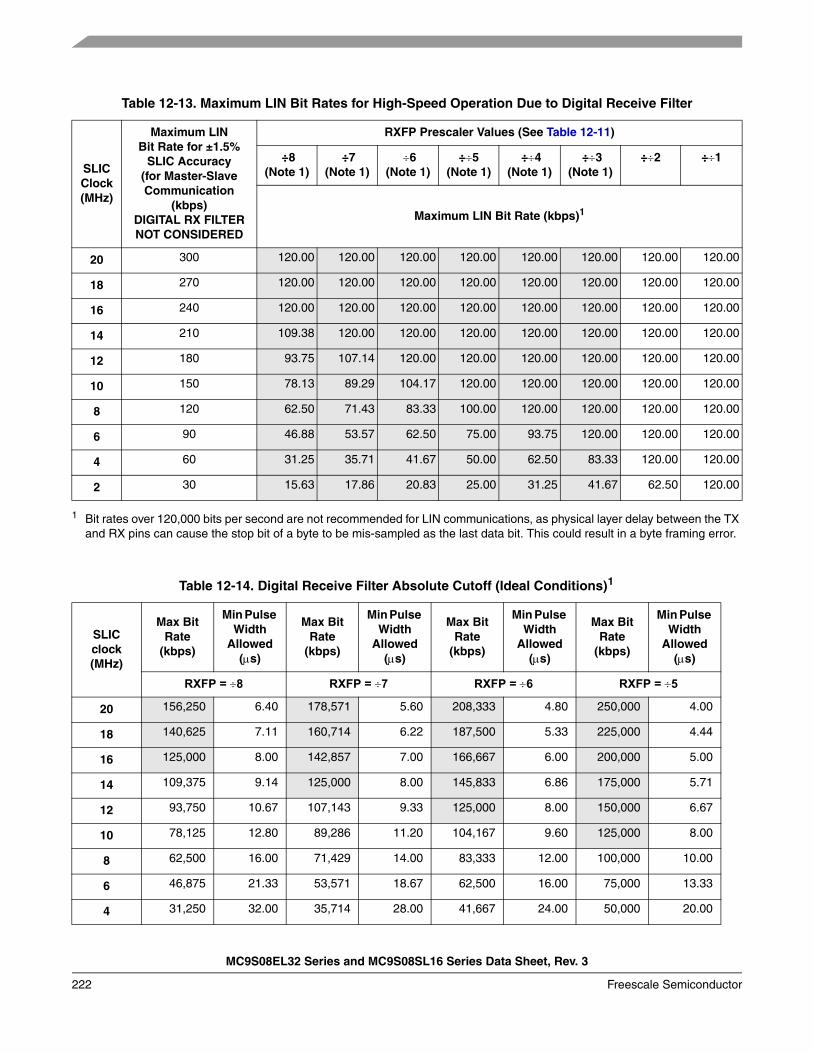
MC9S08EL32 Series and MC9S08SL16 Series Data Sheet, Rev. 3
222 Freescale Semiconductor
Table 12-13. Maximum LIN Bit Rates for High-Speed Operation Due to Digital Receive Filter
SLIC Clock (MHz)
Maximum LINBit Rate for ±1.5%
SLIC Accuracy(for Master-SlaveCommunication
(kbps)DIGITAL RX FILTERNOT CONSIDERED
RXFP Prescaler Values (See Table 12-11)
÷8(Note 1)
÷7(Note 1)
÷6(Note 1)
÷÷5(Note 1)
÷÷4(Note 1)
÷÷3(Note 1)
÷÷2 ÷÷1
Maximum LIN Bit Rate (kbps)1
1 Bit rates over 120,000 bits per second are not recommended for LIN communications, as physical layer delay between the TX and RX pins can cause the stop bit of a byte to be mis-sampled as the last data bit. This could result in a byte framing error.
20 300 120.00 120.00 120.00 120.00 120.00 120.00 120.00 120.00
18 270 120.00 120.00 120.00 120.00 120.00 120.00 120.00 120.00
16 240 120.00 120.00 120.00 120.00 120.00 120.00 120.00 120.00
14 210 109.38 120.00 120.00 120.00 120.00 120.00 120.00 120.00
12 180 93.75 107.14 120.00 120.00 120.00 120.00 120.00 120.00
10 150 78.13 89.29 104.17 120.00 120.00 120.00 120.00 120.00
8 120 62.50 71.43 83.33 100.00 120.00 120.00 120.00 120.00
6 90 46.88 53.57 62.50 75.00 93.75 120.00 120.00 120.00
4 60 31.25 35.71 41.67 50.00 62.50 83.33 120.00 120.00
2 30 15.63 17.86 20.83 25.00 31.25 41.67 62.50 120.00
Table 12-14. Digital Receive Filter Absolute Cutoff (Ideal Conditions)1
SLIC clock (MHz)
Max Bit Rate
(kbps)
Min Pulse Width
Allowed (μs)
Max Bit Rate
(kbps)
Min Pulse Width
Allowed (μs)
Max Bit Rate
(kbps)
Min Pulse Width
Allowed (μs)
Max Bit Rate
(kbps)
Min Pulse Width
Allowed (μs)
RXFP = ÷8 RXFP = ÷7 RXFP = ÷6 RXFP = ÷5
20 156,250 6.40 178,571 5.60 208,333 4.80 250,000 4.00
18 140,625 7.11 160,714 6.22 187,500 5.33 225,000 4.44
16 125,000 8.00 142,857 7.00 166,667 6.00 200,000 5.00
14 109,375 9.14 125,000 8.00 145,833 6.86 175,000 5.71
12 93,750 10.67 107,143 9.33 125,000 8.00 150,000 6.67
10 78,125 12.80 89,286 11.20 104,167 9.60 125,000 8.00
8 62,500 16.00 71,429 14.00 83,333 12.00 100,000 10.00
6 46,875 21.33 53,571 18.67 62,500 16.00 75,000 13.33
4 31,250 32.00 35,714 28.00 41,667 24.00 50,000 20.00
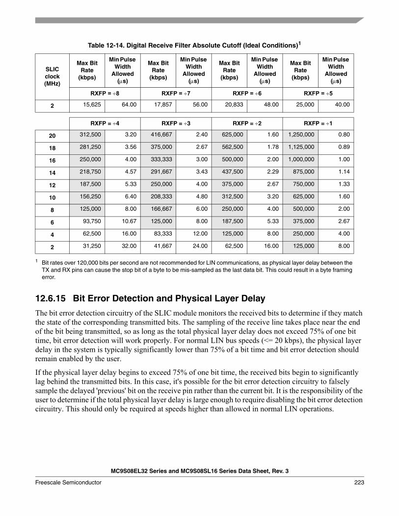
MC9S08EL32 Series and MC9S08SL16 Series Data Sheet, Rev. 3
Freescale Semiconductor 223
12.6.15 Bit Error Detection and Physical Layer Delay
The bit error detection circuitry of the SLIC module monitors the received bits to determine if they match the state of the corresponding transmitted bits. The sampling of the receive line takes place near the end of the bit being transmitted, so as long as the total physical layer delay does not exceed 75% of one bit time, bit error detection will work properly. For normal LIN bus speeds (<= 20 kbps), the physical layer delay in the system is typically significantly lower than 75% of a bit time and bit error detection should remain enabled by the user.
If the physical layer delay begins to exceed 75% of one bit time, the received bits begin to significantly lag behind the transmitted bits. In this case, it's possible for the bit error detection circuitry to falsely sample the delayed 'previous' bit on the receive pin rather than the current bit. It is the responsibility of the user to determine if the total physical layer delay is large enough to require disabling the bit error detection circuitry. This should only be required at speeds higher than allowed in normal LIN operations.
2 15,625 64.00 17,857 56.00 20,833 48.00 25,000 40.00
RXFP = ÷4 RXFP = ÷3 RXFP = ÷2 RXFP = ÷1
20 312,500 3.20 416,667 2.40 625,000 1.60 1,250,000 0.80
18 281,250 3.56 375,000 2.67 562,500 1.78 1,125,000 0.89
16 250,000 4.00 333,333 3.00 500,000 2.00 1,000,000 1.00
14 218,750 4.57 291,667 3.43 437,500 2.29 875,000 1.14
12 187,500 5.33 250,000 4.00 375,000 2.67 750,000 1.33
10 156,250 6.40 208,333 4.80 312,500 3.20 625,000 1.60
8 125,000 8.00 166,667 6.00 250,000 4.00 500,000 2.00
6 93,750 10.67 125,000 8.00 187,500 5.33 375,000 2.67
4 62,500 16.00 83,333 12.00 125,000 8.00 250,000 4.00
2 31,250 32.00 41,667 24.00 62,500 16.00 125,000 8.00
1 Bit rates over 120,000 bits per second are not recommended for LIN communications, as physical layer delay between the TX and RX pins can cause the stop bit of a byte to be mis-sampled as the last data bit. This could result in a byte framing error.
Table 12-14. Digital Receive Filter Absolute Cutoff (Ideal Conditions)1
SLIC clock (MHz)
Max Bit Rate
(kbps)
Min Pulse Width
Allowed (μs)
Max Bit Rate
(kbps)
Min Pulse Width
Allowed (μs)
Max Bit Rate
(kbps)
Min Pulse Width
Allowed (μs)
Max Bit Rate
(kbps)
Min Pulse Width
Allowed (μs)
RXFP = ÷8 RXFP = ÷7 RXFP = ÷6 RXFP = ÷5
MC9S08EL32 Series and MC9S08SL16 Series Data Sheet, Rev. 3
224 Freescale Semiconductor
12.6.16 Byte Transfer Mode Operation
This subsection describes the operation and limitations of the optional UART-like byte transfer mode (BTM). This mode allows sending and receiving individual bytes, but changes the behavior of the SLCBT registers (now read/write registers) and locks the SLCDLC to 1 byte data length. The SLCBT value now becomes the bit time reference for the SLIC, where the software sets the length of one bit time rather than the SLIC module itself. This is similar to an input capture/output compare (IC/OC) count in a timer module, where the count value represents the number of SLIC clock counts in one bit time.
Byte transfer mode assumes that the user has a very stable, precise oscillator, resonator, or clock reference input into the MCU and is therefore not appropriate for use with internal oscillators. There is no synchronization method available to the user in this mode and the user must tell the SLIC how many clock counts comprise a bit time. Figure 12-17, Figure 12-18, Figure 12-19, and Figure 12-20 show calculations to determine the SLCBT value for different settings.
NOTEIt is possible to use the LIN autobauding circuitry in a non-LIN system to derive the correct bit timing values if system constraints allow. To do this the SLIC module must be activated in LIN mode (BTM=0) and receive a break symbol, 0x55 data byte and one additional data byte (at the desired BTM speed). Upon receiving this sequence of symbols which appears to be a LIN header, the SLIC module will assert an ID received successfully interrupt (SLCSV=0x2C). The value in the SLCBT registers will reflect the bit rate which the 0x55 data character was received and can be saved to RAM. The user then switches the SLIC into BTM mode and reloads this value from RAM and the SLIC will be configured to communicate in BTM mode at the baud rate which the 0x55 data character was sent. Care must be taken to ensure that any change between LIN and BTM modes be done at known states in message traffic, such as between message frames, after an ID is successfully received in LIN mode, or when the LIN bus is IDLE as indicated by the SLCACT bit equal to 0.
In the example in Figure 12-17, the user should write 0x16, as a write of 0x15 (decimal value of 21) would automatically revert to 0x14, resulting in transmitted bit times that are 1.33 SLIC clock periods too short rather than 0.667 SLIC clock periods too long. The optimal choice, which gives the smallest resolution error, is the closest even number of SLIC clocks to the exact calculated SLCBT value.
There is a trade-off between maximum bit rate and resolution with the SLIC in BTM mode. Faster SLIC clock speeds improve resolution, but require higher numbers to be written to the SLCBT registers for a given desired bit rate. It is up to the user to determine what level of resolution is acceptable for the given application.
NOTEDo not set the SLCBT registers to a value lower than 16 clock counts for correct operation.
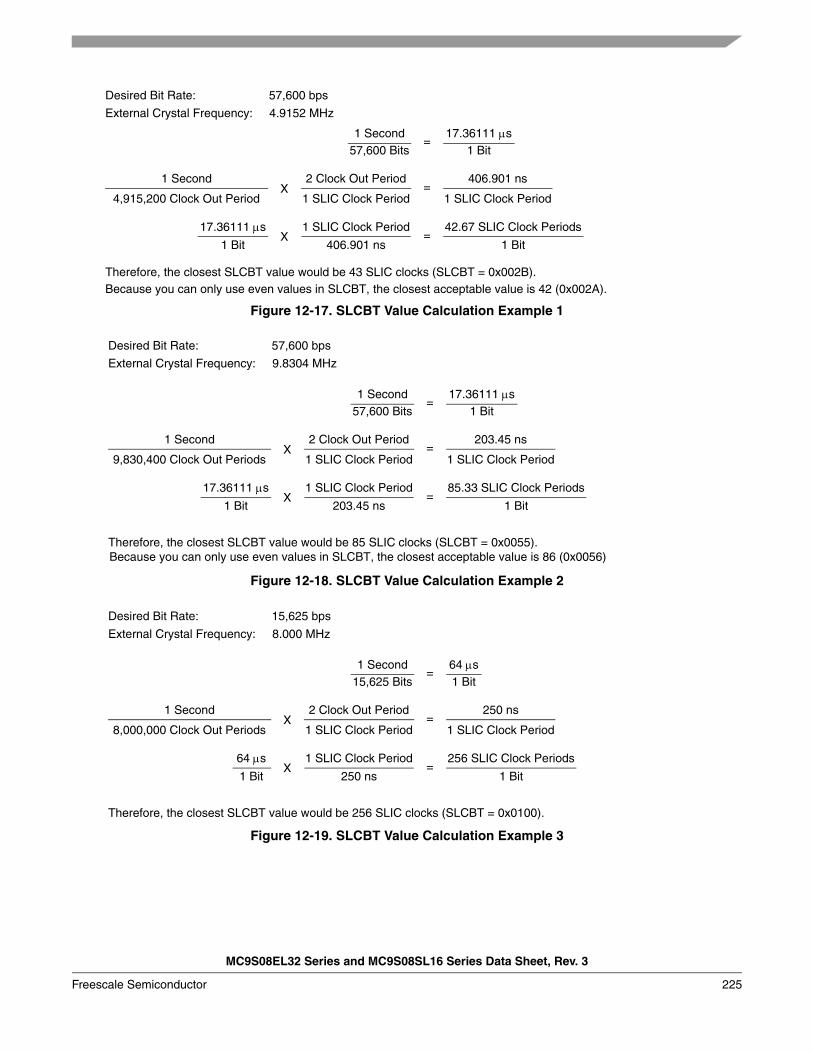
MC9S08EL32 Series and MC9S08SL16 Series Data Sheet, Rev. 3
Freescale Semiconductor 225
Figure 12-17. SLCBT Value Calculation Example 1
Figure 12-18. SLCBT Value Calculation Example 2
Figure 12-19. SLCBT Value Calculation Example 3
2 Clock Out Period
42.67 SLIC Clock Periods
1 SLIC Clock Period
1 SLIC Clock PeriodX =
406.901 ns 1 Bit
1 SLIC Clock Period=
406.901 ns
1 Second57,600 Bits
=17.36111 μs
1 Bit
4,915,200 Clock Out Period
1 SecondX
17.36111 μs
1 Bit
Desired Bit Rate: 57,600 bps
External Crystal Frequency: 4.9152 MHz
Therefore, the closest SLCBT value would be 43 SLIC clocks (SLCBT = 0x002B).Because you can only use even values in SLCBT, the closest acceptable value is 42 (0x002A).
2 Clock Out Period
85.33 SLIC Clock Periods
1 SLIC Clock Period
1 SLIC Clock PeriodX =
203.45 ns 1 Bit
1 SLIC Clock Period=
203.45 ns
1 Second57,600 Bits
=17.36111 μs
1 Bit
9,830,400 Clock Out Periods
1 SecondX
17.36111 μs
1 Bit
Desired Bit Rate: 57,600 bps
External Crystal Frequency: 9.8304 MHz
Therefore, the closest SLCBT value would be 85 SLIC clocks (SLCBT = 0x0055).Because you can only use even values in SLCBT, the closest acceptable value is 86 (0x0056)
2 Clock Out Period
256 SLIC Clock Periods
1 SLIC Clock Period
1 SLIC Clock PeriodX =
250 ns 1 Bit
1 SLIC Clock Period=
250 ns
1 Second15,625 Bits
=64 μs1 Bit
8,000,000 Clock Out Periods
1 SecondX
64 μs
1 Bit
Desired Bit Rate: 15,625 bps
External Crystal Frequency: 8.000 MHz
Therefore, the closest SLCBT value would be 256 SLIC clocks (SLCBT = 0x0100).
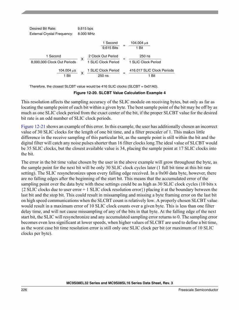
MC9S08EL32 Series and MC9S08SL16 Series Data Sheet, Rev. 3
226 Freescale Semiconductor
Figure 12-20. SLCBT Value Calculation Example 4
This resolution affects the sampling accuracy of the SLIC module on receiving bytes, but only as far as locating the sample point of each bit within a given byte. The best sample point of the bit may be off by as much as one SLIC clock period from the exact center of the bit, if the proper SLCBT value for the desired bit rate is an odd number of SLIC clock periods.
Figure 12-21 shows an example of this error. In this example, the user has additionally chosen an incorrect value of 30 SLIC clocks for the length of one bit time, and a filter prescaler of 1. This makes little difference in the receive sampling of this particular bit, as the sample point is still within the bit and the digital filter will catch any noise pulses shorter than 16 filter clocks long.The ideal value of SLCBT would be 35 SLIC clocks, but the closest available value is 34, placing the sample point at 17 SLIC clocks into the bit.
The error in the bit time value chosen by the user in the above example will grow throughout the byte, as the sample point for the next bit will be only 30 SLIC clock cycles later (1 full bit time at this bit rate setting). The SLIC resynchronizes upon every falling edge received. In a 0x00 data byte, however, there are no falling edges after the beginning of the start bit. This means that the accumulated error of the sampling point over the data byte with these settings could be as high as 30 SLIC clock cycles (10 bits x {2 SLIC clocks due to user error + 1 SLIC clock resolution error}) placing it at the boundary between the last bit and the stop bit. This could result in missampling and missing a byte framing error on the last bit on high speed communications when the SLCBT count is relatively low. A properly chosen SLCBT value would result in a maximum error of 10 SLIC clock counts over a given byte. This is less than one filter delay time, and will not cause missampling of any of the bits in that byte. At the falling edge of the next start bit, the SLIC will resynchronize and any accumulated sampling error returns to 0. The sampling error becomes even less significant at lower speeds, when higher values of SLCBT are used to define a bit time, as the worst case bit time resolution error is still only one SLIC clock per bit (or maximum of 10 SLIC clocks per byte).
2 Clock Out Period
416.017 SLIC Clock Periods
1 SLIC Clock Period
1 SLIC Clock PeriodX =
250 ns 1 Bit
1 SLIC Clock Period=
250 ns
1 Second9,615 Bits
=104.004 μs
1 Bit
8,000,000 Clock Out Periods
1 SecondX
104.004 μs
1 Bit
Desired Bit Rate: 9,615 bps
External Crystal Frequency: 8.000 MHz
Therefore, the closest SLCBT value would be 416 SLIC clocks (SLCBT = 0x01A0).
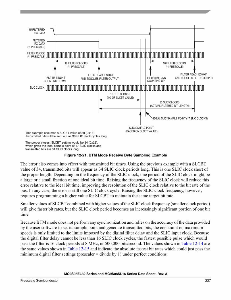
MC9S08EL32 Series and MC9S08SL16 Series Data Sheet, Rev. 3
Freescale Semiconductor 227
Figure 12-21. BTM Mode Receive Byte Sampling Example
The error also comes into effect with transmitted bit times. Using the previous example with a SLCBT value of 34, transmitted bits will appear as 34 SLIC clock periods long. This is one SLIC clock short of the proper length. Depending on the frequency of the SLIC clock, one period of the SLIC clock might be a large or a small fraction of one ideal bit time. Raising the frequency of the SLIC clock will reduce this error relative to the ideal bit time, improving the resolution of the SLIC clock relative to the bit rate of the bus. In any case, the error is still one SLIC clock cycle. Raising the SLIC clock frequency, however, requires programming a higher value for SLCBT to maintain the same target bit rate.
Smaller values of SLCBT combined with higher values of the SLIC clock frequency (smaller clock period) will give faster bit rates, but the SLIC clock period becomes an increasingly significant portion of one bit time.
Because BTM mode does not perform any synchronization and relies on the accuracy of the data provided by the user software to set its sample point and generate transmitted bits, the constraint on maximum speeds is only limited to the limits imposed by the digital filter delay and the SLIC input clock. Because the digital filter delay cannot be less than 16 SLIC clock cycles, the fastest possible pulse which would pass the filter is 16 clock periods at 8 MHz, or 500,000 bits/second. The values shown in Table 12-14 are the same values shown in Table 12-15 and indicate the absolute fastest bit rates which could just pass the minimum digital filter settings (prescaler = divide by 1) under perfect conditions.
FILTEREDRX DATA
FILTER CLOCK
UNFILTEREDRX DATA
16 FILTER CLOCKS
(³1 PRESCALE)
FILTER BEGINS FILTER REACHES 0X0
FILTER BEGINSFILTER REACHES 0XF
AND TOGGLES FILTER OUTPUTAND TOGGLES FILTER OUTPUT
SLIC CLOCK
(³1 PRESCALE)
15 SLIC CLOCKS
COUNTING UP
35 SLIC CLOCKS
COUNTING DOWN
SLIC SAMPLE POINT(BASED ON SLCBT VALUE)This example assumes a SLCBT value of 30 (0x1E).
IDEAL SLIC SAMPLE POINT (17 SLIC CLOCKS)
Transmitted bits will be sent out as 30 SLIC clock cycles long.
The proper closest SLCBT setting would be 34 (0x22), which gives the ideal sample point of 17 SLIC clocks andtransmitted bits are 34 SLIC clocks long.
(³1 PRESCALE)16 FILTER CLOCKS
(³1 PRESCALE)
(1/2 OF SLCBT VALUE)
(ACTUAL FILTERED BIT LENGTH)
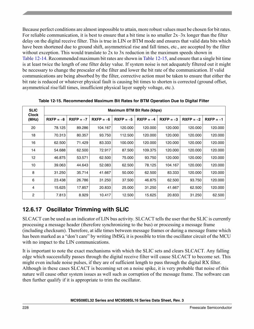
MC9S08EL32 Series and MC9S08SL16 Series Data Sheet, Rev. 3
228 Freescale Semiconductor
Because perfect conditions are almost impossible to attain, more robust values must be chosen for bit rates. For reliable communication, it is best to ensure that a bit time is no smaller 2x–3x longer than the filter delay on the digital receive filter. This is true in LIN or BTM mode and ensures that valid data bits which have been shortened due to ground shift, asymmetrical rise and fall times, etc., are accepted by the filter without exception. This would translate to 2x to 3x reduction in the maximum speeds shown in Table 12-14. Recommended maximum bit rates are shown in Table 12-15, and ensure that a single bit time is at least twice the length of one filter delay value. If system noise is not adequately filtered out it might be necessary to change the prescaler of the filter and lower the bit rate of the communication. If valid communications are being absorbed by the filter, corrective action must be taken to ensure that either the bit rate is reduced or whatever physical fault is causing bit times to shorten is corrected (ground offset, asymmetrical rise/fall times, insufficient physical layer supply voltage, etc.).
12.6.17 Oscillator Trimming with SLIC
SLCACT can be used as an indicator of LIN bus activity. SLCACT tells the user that the SLIC is currently processing a message header (therefore synchronizing to the bus) or processing a message frame (including checksum). Therefore, at idle times between message frames or during a message frame which has been marked as a “don’t care” by writing IMSG, it is possible to trim the oscillator circuit of the MCU with no impact to the LIN communications.
It is important to note the exact mechanisms with which the SLIC sets and clears SLCACT. Any falling edge which successfully passes through the digital receive filter will cause SLCACT to become set. This might even include noise pulses, if they are of sufficient length to pass through the digital RX filter. Although in these cases SLCACT is becoming set on a noise spike, it is very probable that noise of this nature will cause other system issues as well such as corruption of the message frame. The software can then further qualify if it is appropriate to trim the oscillator.
Table 12-15. Recommended Maximum Bit Rates for BTM Operation Due to Digital Filter
SLIC Clock (MHz)
Maximum BTM Bit Rate (kbps)
RXFP = ÷8 RXFP = ÷7 RXFP = ÷6 RXFP = ÷5 RXFP = ÷4 RXFP = ÷3 RXFP = ÷2 RXFP = ÷1
20 78.125 89.286 104.167 120.000 120.000 120.000 120.000 120.000
18 70.313 80.357 93.750 112.500 120.000 120.000 120.000 120.000
16 62.500 71.429 83.333 100.000 120.000 120.000 120.000 120.000
14 54.688 62.500 72.917 87.500 109.375 120.000 120.000 120.000
12 46.875 53.571 62.500 75.000 93.750 120.000 120.000 120.000
10 39.063 44.643 52.083 62.500 78.125 104.167 120.000 120.000
8 31.250 35.714 41.667 50.000 62.500 83.333 120.000 120.000
6 23.438 26.786 31.250 37.500 46.875 62.500 93.750 120.000
4 15.625 17.857 20.833 25.000 31.250 41.667 62.500 120.000
2 7.813 8.929 10.417 12.500 15.625 20.833 31.250 62.500
MC9S08EL32 Series and MC9S08SL16 Series Data Sheet, Rev. 3
Freescale Semiconductor 229
SLCACT will only be cleared by the SLIC upon successful completion of a normal LIN message frame (see Section , “,” description for more detail). This means that in some cases, if a message frame terminates with an error condition or some source other than those cited in the SLCACT bit description, SLCACT might remain set during an otherwise idle bus time. SLCACT will then clear upon the successful completion of the next LIN message frame.
These mechanisms might result in SLCACT being set when it is safe (from the SLIC module perspective) to trim the oscillator. However, SLCACT will only be clear when the SLIC considers it safe to trim the oscillator.
In a particular system, it might also be possible to improve the opportunities for trimming by using system knowledge and use of IMSG. If a message ID is known to be considered a “don’t care” by this particular node, it should be safe to trim the oscillator during that message frame (provided that it is safe for the application software as well). After the software has done an identifier lookup and determined that the ID corresponds to a “don’t care” message, the software might choose to set IMSG. From that time, the application software should have at least one byte time of message traffic in which to trim the oscillator before that ignored message frame expires, regardless of the state of SLCACT. If the length of that ignored message frame is known, that knowledge might also be used to extend the time of this oscillator trimming opportunity.
Now that the mechanisms for recognizing when the SLIC module indicates safe oscillator trimming opportunities are understood, it is important to understand how to derive the information needed to perform the trimming.
The value in SLCBT will indicate how many SLIC clock cycles comprise one bit time and for any given LIN bus speed, this will be a fixed value if the oscillator is running at its ideal frequency. It is possible to use this ideal value combined with the measured value in SLCBT to determine how to adjust the oscillator of the microcontroller.
The actual oscillator trimming algorithm is very specific to each particular implementation, and applications might or might not require the oscillator even to be trimmed. The SLIC can maintain communications even with input oscillator variation of ±50% (with 4 MHz nominal, that means that any input clock into the SLIC from 2 MHz to 6 MHz will still guarantee communications). Because Freescale internal oscillators are at least within ±25% of their nominal value, even when untrimmed, this means that trimming of the oscillator is not even required for LIN communications. If the application can tolerate the range of frequencies which might appear within this manufacturing range, then it is not necessary ever to trim the oscillator. This can be a tremendous advantage to the customer, enabling migration to very low-cost ROM devices which have no non-volatile memory in which to store the trim value.
NOTEEven though most internal oscillators are within ±25% before trimming, they are stable at some frequency in that range, within at least ±5% over the entire operating voltage and temperature range. The trimming operation simply eliminates the offset due to factory manufacturing variations to re-center the base oscillator frequency to the nominal value. Please refer to the electrical specifications for the oscillator for more specific information, as exact specifications might differ from module to module.
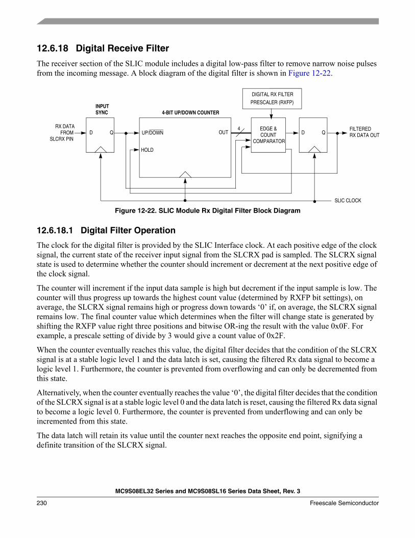
MC9S08EL32 Series and MC9S08SL16 Series Data Sheet, Rev. 3
230 Freescale Semiconductor
12.6.18 Digital Receive Filter
The receiver section of the SLIC module includes a digital low-pass filter to remove narrow noise pulses from the incoming message. A block diagram of the digital filter is shown in Figure 12-22.
Figure 12-22. SLIC Module Rx Digital Filter Block Diagram
12.6.18.1 Digital Filter Operation
The clock for the digital filter is provided by the SLIC Interface clock. At each positive edge of the clock signal, the current state of the receiver input signal from the SLCRX pad is sampled. The SLCRX signal state is used to determine whether the counter should increment or decrement at the next positive edge of the clock signal.
The counter will increment if the input data sample is high but decrement if the input sample is low. The counter will thus progress up towards the highest count value (determined by RXFP bit settings), on average, the SLCRX signal remains high or progress down towards ‘0’ if, on average, the SLCRX signal remains low. The final counter value which determines when the filter will change state is generated by shifting the RXFP value right three positions and bitwise OR-ing the result with the value 0x0F. For example, a prescale setting of divide by 3 would give a count value of 0x2F.
When the counter eventually reaches this value, the digital filter decides that the condition of the SLCRX signal is at a stable logic level 1 and the data latch is set, causing the filtered Rx data signal to become a logic level 1. Furthermore, the counter is prevented from overflowing and can only be decremented from this state.
Alternatively, when the counter eventually reaches the value ‘0’, the digital filter decides that the condition of the SLCRX signal is at a stable logic level 0 and the data latch is reset, causing the filtered Rx data signal to become a logic level 0. Furthermore, the counter is prevented from underflowing and can only be incremented from this state.
The data latch will retain its value until the counter next reaches the opposite end point, signifying a definite transition of the SLCRX signal.
D Q UP/DOWN OUT4 EDGE &
COUNTCOMPARATOR
D QFILTEREDRX DATA OUT
SLIC CLOCK
RX DATAFROM
SLCRX PIN
INPUTSYNC 4-BIT UP/DOWN COUNTER
DIGITAL RX FILTER
PRESCALER (RXFP)
HOLD
MC9S08EL32 Series and MC9S08SL16 Series Data Sheet, Rev. 3
Freescale Semiconductor 231
12.6.18.2 Digital Filter Performance
The performance of the digital filter is best described in the time domain rather than the frequency domain.
If the signal on the SLCRX signal transitions, then there will be a delay before that transition appears at the filtered Rx data output signal. This delay will be between 15 and 16 clock periods, depending on where the transition occurs with respect to the sampling points. This ‘filter delay’ is not an issue for SLIC operation, as there is no need for message arbitration.
The effect of random noise on the SLCRX signal depends on the characteristics of the noise itself. Narrow noise pulses on the SLCRX signal will be completely ignored if they are shorter than the filter delay. This provides a degree of low-pass filtering. Figure 12-22 shows the configuration of the digital receive filter and the consequential effect on the filter delay. This filter delay value indicates that for a particular setup, only pulses of which are greater than the filter delay will pass the filter.
For example, if the frequency of the SLIC clock (fSLIC) is 3.2 MHz, then the period (tSLIC) is of the SLIC clock is 313 ns. With a receive filter prescaler setting of division by 3, the resulting maximum filter delay in the absence of noise will be 15.00 μs. By simply changing the prescaler of the receive filter, the user can then select alternatively 5 μs, 10 μs, or 20 μs as a minimum filter delay according to the systems requirements.
If noise occurs during a symbol transition, the detection of that transition may be delayed by an amount equal to the length of the noise burst. This is just a reflection of the uncertainty of where the transition is truly occurring within the noise.
NOTEThe user must always account for the worst case bit timing of their LIN bus when configuring the digital receive filter, especially if running at faster speeds. Ground offset and other physical layer conditions can cause shortening of bits as seen at the digital receive pin, for example. If these shortened bit lengths are less than the filter delay, the bits will be interpreted by the filter as noise and will be blocked, even though the nominal bit timing might be greater than the filter delay.

MC9S08EL32 Series and MC9S08SL16 Series Data Sheet, Rev. 3
232 Freescale Semiconductor
MC9S08EL32 Series and MC9S08SL16 Series Data Sheet, Rev. 3
Freescale Semiconductor 233
Chapter 13 Serial Peripheral Interface (S08SPIV3)
13.1 IntroductionThe serial peripheral interface (SPI) module provides full-duplex, synchronous, serial communication between the MCU and peripheral devices. These peripheral devices can include other microcontrollers, analog-to-digital converters, shift registers, sensors, memories, and so forth.
The maximum SPI baud rate depends on the operating mode:• Master mode — bus clock divided by two• Slave mode — bus clock divided by four
The SPI operation can be driven by interrupts or software can poll the status flags.
All devices in the MC9S08EL32 Series and MC9S08SL16 Series MCUs contain one SPI module Figure 13-1 highlights the SPI module.
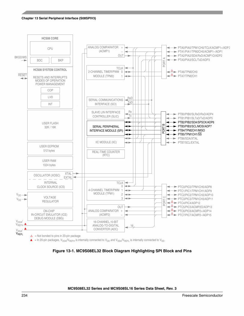
Chapter 13 Serial Peripheral Interface (S08SPIV3)
MC9S08EL32 Series and MC9S08SL16 Series Data Sheet, Rev. 3
234 Freescale Semiconductor
Figure 13-1. MC9S08EL32 Block Diagram Highlighting SPI Block and Pins
VSS
IIC MODULE (IIC)
SERIAL PERIPHERAL INTERFACE MODULE (SPI)
USER FLASH
USER RAM
32K / 16K
HCS08 CORE
CPU
BDC
2-CHANNEL TIMER/PWMMODULE (TPM2)
HCS08 SYSTEM CONTROL
RESETS AND INTERRUPTSMODES OF OPERATIONPOWER MANAGEMENT
VOLTAGE REGULATOR
COP
LVD
OSCILLATOR (XOSC)
INTERNALCLOCK SOURCE (ICS)
RESET
VREFH
1024 bytes
INTERFACE (SCI)SERIAL COMMUNICATIONS
XTALEXTAL
4-CHANNEL TIMER/PWMMODULE (TPM1)
REAL-TIME COUNTER
IN-CIRCUIT EMULATOR (ICE)
BKGD/MS PTA3/PIA3/SCL/TxD/ADP3
PTA6/TPM2CH0
PTA2/PIA2/SDA/RxD/ACMP1O/ADP2PTA1/PIA1/TPM2CH0/ACMP1–/ADP1PTA0/PIA0/TPM1CH0/TCLK/ACMP1+/ADP0
PTA7/TPM2CH1
PTB3/PIB3/SCL/MOSI/ADP7PTB4/TPM2CH1/MISO
PTB2/PIB2/SDA/SPSCK/ADP6PTB1/PIB1/SLTxD/TxD/ADP5PTB0/PIB0/SLRxD/RxD/ADP4
PTB7/SCL/EXTAL
PTC3/PIC3/TPM1CH3/ADP11PTC4/PIC4/ADP12PTC5/PIC5/ACMP2O/ADP13
PTC2/PIC2/TPM1CH2/ADP10PTC1/PIC1/TPM1CH1/ADP9
POR
T C
PTC6/PIC6/ACMP2+/ADP14
VDD
BKP
INT
ANALOG COMPARATOR(ACMP2)
USER EEPROM512 bytes
CONTROLLER (SLIC)SLAVE LIN INTERFACE
ANALOG-TO-DIGITALCONVERTER (ADC)
16-CHANNEL,10-BIT16
= In 20-pin packages, VDDA/VREFH is internally connected to VDD and VSSA/VREFL is internally connected to VSS.
VDDA/
VREFL
VSSA/
DEBUG MODULE (DBG)
ON-CHIP
(RTC)
PTC0/PIC0/TPM1CH0/ADP8
PTC7/PIC7/ACMP2–/ADP15
PTB6/SDA/XTAL
POR
T B
POR
T A
PTB5/TPM1CH1/SS
ANALOG COMPARATOR(ACMP1)
= Not bonded to pins in 20-pin package
TCLK
TCLK
+–
OUT
+–
OUT
0123
10
RxDTxD
TxRx
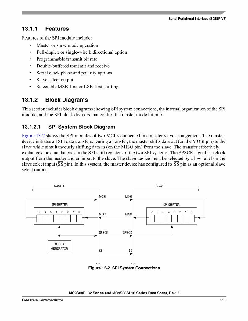
Serial Peripheral Interface (S08SPIV3)
MC9S08EL32 Series and MC9S08SL16 Series Data Sheet, Rev. 3
Freescale Semiconductor 235
13.1.1 Features
Features of the SPI module include:• Master or slave mode operation• Full-duplex or single-wire bidirectional option• Programmable transmit bit rate• Double-buffered transmit and receive• Serial clock phase and polarity options• Slave select output• Selectable MSB-first or LSB-first shifting
13.1.2 Block Diagrams
This section includes block diagrams showing SPI system connections, the internal organization of the SPI module, and the SPI clock dividers that control the master mode bit rate.
13.1.2.1 SPI System Block Diagram
Figure 13-2 shows the SPI modules of two MCUs connected in a master-slave arrangement. The master device initiates all SPI data transfers. During a transfer, the master shifts data out (on the MOSI pin) to the slave while simultaneously shifting data in (on the MISO pin) from the slave. The transfer effectively exchanges the data that was in the SPI shift registers of the two SPI systems. The SPSCK signal is a clock output from the master and an input to the slave. The slave device must be selected by a low level on the slave select input (SS pin). In this system, the master device has configured its SS pin as an optional slave select output.
Figure 13-2. SPI System Connections
7 6 5 4 3 2 1 0
SPI SHIFTER
CLOCKGENERATOR
7 6 5 4 3 2 1 0
SPI SHIFTER
SS
SPSCK
MISO
MOSI
SS
SPSCK
MISO
MOSI
MASTER SLAVE
Serial Peripheral Interface (S08SPIV3)
MC9S08EL32 Series and MC9S08SL16 Series Data Sheet, Rev. 3
236 Freescale Semiconductor
The most common uses of the SPI system include connecting simple shift registers for adding input or output ports or connecting small peripheral devices such as serial A/D or D/A converters. Although Figure 13-2 shows a system where data is exchanged between two MCUs, many practical systems involve simpler connections where data is unidirectionally transferred from the master MCU to a slave or from a slave to the master MCU.
13.1.2.2 SPI Module Block Diagram
Figure 13-3 is a block diagram of the SPI module. The central element of the SPI is the SPI shift register. Data is written to the double-buffered transmitter (write to SPID) and gets transferred to the SPI shift register at the start of a data transfer. After shifting in a byte of data, the data is transferred into the double-buffered receiver where it can be read (read from SPID). Pin multiplexing logic controls connections between MCU pins and the SPI module.
When the SPI is configured as a master, the clock output is routed to the SPSCK pin, the shifter output is routed to MOSI, and the shifter input is routed from the MISO pin.
When the SPI is configured as a slave, the SPSCK pin is routed to the clock input of the SPI, the shifter output is routed to MISO, and the shifter input is routed from the MOSI pin.
In the external SPI system, simply connect all SPSCK pins to each other, all MISO pins together, and all MOSI pins together. Peripheral devices often use slightly different names for these pins.
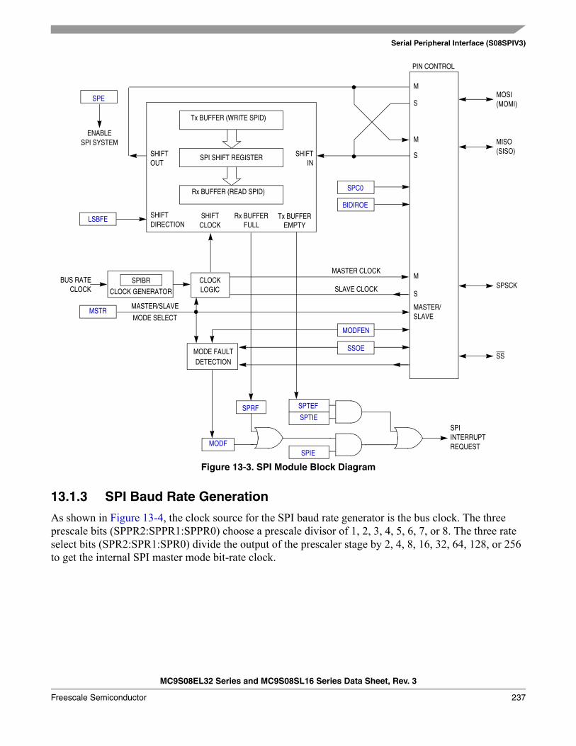
Serial Peripheral Interface (S08SPIV3)
MC9S08EL32 Series and MC9S08SL16 Series Data Sheet, Rev. 3
Freescale Semiconductor 237
Figure 13-3. SPI Module Block Diagram
13.1.3 SPI Baud Rate Generation
As shown in Figure 13-4, the clock source for the SPI baud rate generator is the bus clock. The three prescale bits (SPPR2:SPPR1:SPPR0) choose a prescale divisor of 1, 2, 3, 4, 5, 6, 7, or 8. The three rate select bits (SPR2:SPR1:SPR0) divide the output of the prescaler stage by 2, 4, 8, 16, 32, 64, 128, or 256 to get the internal SPI master mode bit-rate clock.
SPI SHIFT REGISTER
SHIFTCLOCK
SHIFTDIRECTION
Rx BUFFERFULL
Tx BUFFEREMPTY
SHIFTOUT
SHIFTIN
ENABLESPI SYSTEM
CLOCKLOGICCLOCK GENERATOR
BUS RATECLOCK
MASTER/SLAVE
MODE SELECT
MODE FAULTDETECTION
MASTER CLOCK
SLAVE CLOCK
SPIINTERRUPTREQUEST
PIN CONTROL
M
S
MASTER/SLAVE
MOSI(MOMI)
MISO(SISO)
SPSCK
SS
M
S
S
M
MODF
SPE
LSBFE
MSTR
SPRF SPTEF
SPTIE
SPIE
MODFEN
SSOE
SPC0
BIDIROE
SPIBR
Tx BUFFER (WRITE SPID)
Rx BUFFER (READ SPID)
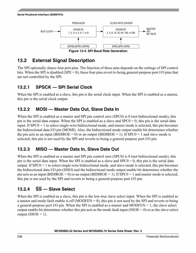
Serial Peripheral Interface (S08SPIV3)
MC9S08EL32 Series and MC9S08SL16 Series Data Sheet, Rev. 3
238 Freescale Semiconductor
Figure 13-4. SPI Baud Rate Generation
13.2 External Signal DescriptionThe SPI optionally shares four port pins. The function of these pins depends on the settings of SPI control bits. When the SPI is disabled (SPE = 0), these four pins revert to being general-purpose port I/O pins that are not controlled by the SPI.
13.2.1 SPSCK — SPI Serial Clock
When the SPI is enabled as a slave, this pin is the serial clock input. When the SPI is enabled as a master, this pin is the serial clock output.
13.2.2 MOSI — Master Data Out, Slave Data In
When the SPI is enabled as a master and SPI pin control zero (SPC0) is 0 (not bidirectional mode), this pin is the serial data output. When the SPI is enabled as a slave and SPC0 = 0, this pin is the serial data input. If SPC0 = 1 to select single-wire bidirectional mode, and master mode is selected, this pin becomes the bidirectional data I/O pin (MOMI). Also, the bidirectional mode output enable bit determines whether the pin acts as an input (BIDIROE = 0) or an output (BIDIROE = 1). If SPC0 = 1 and slave mode is selected, this pin is not used by the SPI and reverts to being a general-purpose port I/O pin.
13.2.3 MISO — Master Data In, Slave Data Out
When the SPI is enabled as a master and SPI pin control zero (SPC0) is 0 (not bidirectional mode), this pin is the serial data input. When the SPI is enabled as a slave and SPC0 = 0, this pin is the serial data output. If SPC0 = 1 to select single-wire bidirectional mode, and slave mode is selected, this pin becomes the bidirectional data I/O pin (SISO) and the bidirectional mode output enable bit determines whether the pin acts as an input (BIDIROE = 0) or an output (BIDIROE = 1). If SPC0 = 1 and master mode is selected, this pin is not used by the SPI and reverts to being a general-purpose port I/O pin.
13.2.4 SS — Slave Select
When the SPI is enabled as a slave, this pin is the low-true slave select input. When the SPI is enabled as a master and mode fault enable is off (MODFEN = 0), this pin is not used by the SPI and reverts to being a general-purpose port I/O pin. When the SPI is enabled as a master and MODFEN = 1, the slave select output enable bit determines whether this pin acts as the mode fault input (SSOE = 0) or as the slave select output (SSOE = 1).
DIVIDE BY2, 4, 8, 16, 32, 64, 128, or 256
DIVIDE BY1, 2, 3, 4, 5, 6, 7, or 8
PRESCALER CLOCK RATE DIVIDER
SPPR2:SPPR1:SPPR0 SPR2:SPR1:SPR0
BUS CLOCKMASTERSPIBIT RATE
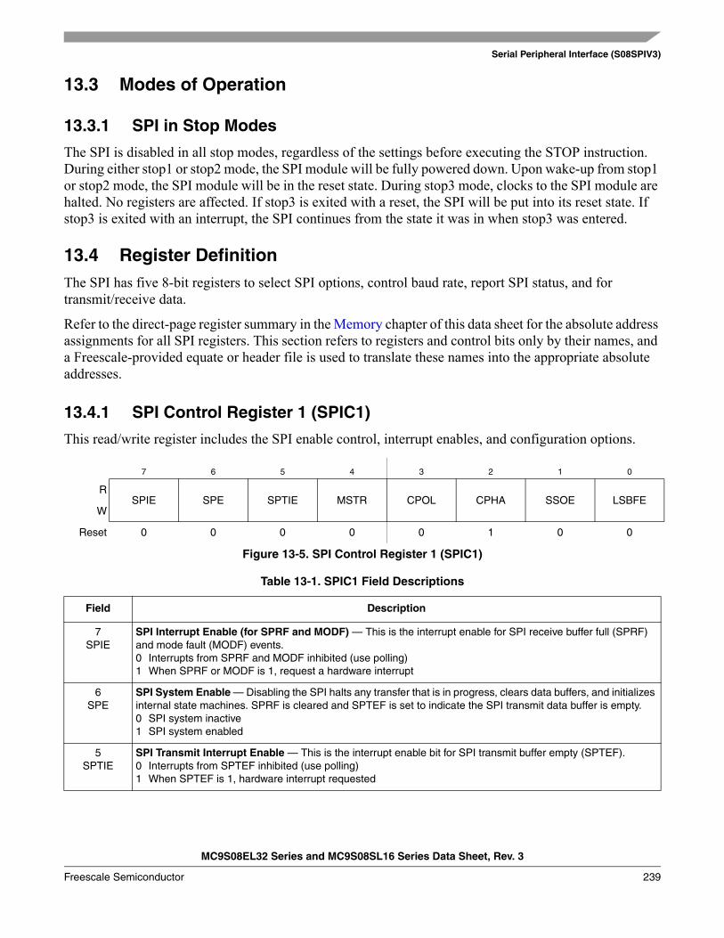
Serial Peripheral Interface (S08SPIV3)
MC9S08EL32 Series and MC9S08SL16 Series Data Sheet, Rev. 3
Freescale Semiconductor 239
13.3 Modes of Operation
13.3.1 SPI in Stop Modes
The SPI is disabled in all stop modes, regardless of the settings before executing the STOP instruction. During either stop1 or stop2 mode, the SPI module will be fully powered down. Upon wake-up from stop1 or stop2 mode, the SPI module will be in the reset state. During stop3 mode, clocks to the SPI module are halted. No registers are affected. If stop3 is exited with a reset, the SPI will be put into its reset state. If stop3 is exited with an interrupt, the SPI continues from the state it was in when stop3 was entered.
13.4 Register DefinitionThe SPI has five 8-bit registers to select SPI options, control baud rate, report SPI status, and for transmit/receive data.
Refer to the direct-page register summary in the Memory chapter of this data sheet for the absolute address assignments for all SPI registers. This section refers to registers and control bits only by their names, and a Freescale-provided equate or header file is used to translate these names into the appropriate absolute addresses.
13.4.1 SPI Control Register 1 (SPIC1)
This read/write register includes the SPI enable control, interrupt enables, and configuration options.
7 6 5 4 3 2 1 0
RSPIE SPE SPTIE MSTR CPOL CPHA SSOE LSBFE
W
Reset 0 0 0 0 0 1 0 0
Figure 13-5. SPI Control Register 1 (SPIC1)
Table 13-1. SPIC1 Field Descriptions
Field Description
7SPIE
SPI Interrupt Enable (for SPRF and MODF) — This is the interrupt enable for SPI receive buffer full (SPRF) and mode fault (MODF) events.0 Interrupts from SPRF and MODF inhibited (use polling)1 When SPRF or MODF is 1, request a hardware interrupt
6SPE
SPI System Enable — Disabling the SPI halts any transfer that is in progress, clears data buffers, and initializes internal state machines. SPRF is cleared and SPTEF is set to indicate the SPI transmit data buffer is empty.0 SPI system inactive1 SPI system enabled
5SPTIE
SPI Transmit Interrupt Enable — This is the interrupt enable bit for SPI transmit buffer empty (SPTEF).0 Interrupts from SPTEF inhibited (use polling)1 When SPTEF is 1, hardware interrupt requested
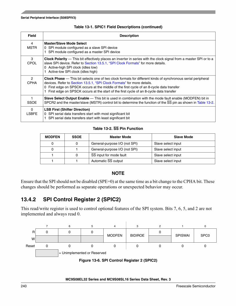
Serial Peripheral Interface (S08SPIV3)
MC9S08EL32 Series and MC9S08SL16 Series Data Sheet, Rev. 3
240 Freescale Semiconductor
NOTE
Ensure that the SPI should not be disabled (SPE=0) at the same time as a bit change to the CPHA bit. These changes should be performed as separate operations or unexpected behavior may occur.
13.4.2 SPI Control Register 2 (SPIC2)
This read/write register is used to control optional features of the SPI system. Bits 7, 6, 5, and 2 are not implemented and always read 0.
4MSTR
Master/Slave Mode Select0 SPI module configured as a slave SPI device1 SPI module configured as a master SPI device
3CPOL
Clock Polarity — This bit effectively places an inverter in series with the clock signal from a master SPI or to a slave SPI device. Refer to Section 13.5.1, “SPI Clock Formats” for more details.0 Active-high SPI clock (idles low)1 Active-low SPI clock (idles high)
2CPHA
Clock Phase — This bit selects one of two clock formats for different kinds of synchronous serial peripheral devices. Refer to Section 13.5.1, “SPI Clock Formats” for more details.0 First edge on SPSCK occurs at the middle of the first cycle of an 8-cycle data transfer1 First edge on SPSCK occurs at the start of the first cycle of an 8-cycle data transfer
1SSOE
Slave Select Output Enable — This bit is used in combination with the mode fault enable (MODFEN) bit in SPCR2 and the master/slave (MSTR) control bit to determine the function of the SS pin as shown in Table 13-2.
0LSBFE
LSB First (Shifter Direction)0 SPI serial data transfers start with most significant bit1 SPI serial data transfers start with least significant bit
Table 13-2. SS Pin Function
MODFEN SSOE Master Mode Slave Mode
0 0 General-purpose I/O (not SPI) Slave select input
0 1 General-purpose I/O (not SPI) Slave select input
1 0 SS input for mode fault Slave select input
1 1 Automatic SS output Slave select input
7 6 5 4 3 2 1 0
R 0 0 0MODFEN BIDIROE
0SPISWAI SPC0
W
Reset 0 0 0 0 0 0 0 0
= Unimplemented or Reserved
Figure 13-6. SPI Control Register 2 (SPIC2)
Table 13-1. SPIC1 Field Descriptions (continued)
Field Description
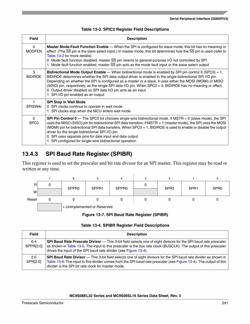
Serial Peripheral Interface (S08SPIV3)
MC9S08EL32 Series and MC9S08SL16 Series Data Sheet, Rev. 3
Freescale Semiconductor 241
13.4.3 SPI Baud Rate Register (SPIBR)
This register is used to set the prescaler and bit rate divisor for an SPI master. This register may be read or written at any time.
Table 13-3. SPIC2 Register Field Descriptions
Field Description
4MODFEN
Master Mode-Fault Function Enable — When the SPI is configured for slave mode, this bit has no meaning or effect. (The SS pin is the slave select input.) In master mode, this bit determines how the SS pin is used (refer to Table 13-2 for more details).0 Mode fault function disabled, master SS pin reverts to general-purpose I/O not controlled by SPI1 Mode fault function enabled, master SS pin acts as the mode fault input or the slave select output
3BIDIROE
Bidirectional Mode Output Enable — When bidirectional mode is enabled by SPI pin control 0 (SPC0) = 1, BIDIROE determines whether the SPI data output driver is enabled to the single bidirectional SPI I/O pin. Depending on whether the SPI is configured as a master or a slave, it uses either the MOSI (MOMI) or MISO (SISO) pin, respectively, as the single SPI data I/O pin. When SPC0 = 0, BIDIROE has no meaning or effect.0 Output driver disabled so SPI data I/O pin acts as an input1 SPI I/O pin enabled as an output
1SPISWAI
SPI Stop in Wait Mode0 SPI clocks continue to operate in wait mode1 SPI clocks stop when the MCU enters wait mode
0SPC0
SPI Pin Control 0 — The SPC0 bit chooses single-wire bidirectional mode. If MSTR = 0 (slave mode), the SPI uses the MISO (SISO) pin for bidirectional SPI data transfers. If MSTR = 1 (master mode), the SPI uses the MOSI (MOMI) pin for bidirectional SPI data transfers. When SPC0 = 1, BIDIROE is used to enable or disable the output driver for the single bidirectional SPI I/O pin.0 SPI uses separate pins for data input and data output1 SPI configured for single-wire bidirectional operation
7 6 5 4 3 2 1 0
R 0SPPR2 SPPR1 SPPR0
0SPR2 SPR1 SPR0
W
Reset 0 0 0 0 0 0 0 0
= Unimplemented or Reserved
Figure 13-7. SPI Baud Rate Register (SPIBR)
Table 13-4. SPIBR Register Field Descriptions
Field Description
6:4SPPR[2:0]
SPI Baud Rate Prescale Divisor — This 3-bit field selects one of eight divisors for the SPI baud rate prescaler as shown in Table 13-5. The input to this prescaler is the bus rate clock (BUSCLK). The output of this prescaler drives the input of the SPI baud rate divider (see Figure 13-4).
2:0SPR[2:0]
SPI Baud Rate Divisor — This 3-bit field selects one of eight divisors for the SPI baud rate divider as shown in Table 13-6. The input to this divider comes from the SPI baud rate prescaler (see Figure 13-4). The output of this divider is the SPI bit rate clock for master mode.
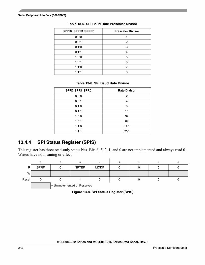
Serial Peripheral Interface (S08SPIV3)
MC9S08EL32 Series and MC9S08SL16 Series Data Sheet, Rev. 3
242 Freescale Semiconductor
13.4.4 SPI Status Register (SPIS)
This register has three read-only status bits. Bits 6, 3, 2, 1, and 0 are not implemented and always read 0. Writes have no meaning or effect.
Table 13-5. SPI Baud Rate Prescaler Divisor
SPPR2:SPPR1:SPPR0 Prescaler Divisor
0:0:0 1
0:0:1 2
0:1:0 3
0:1:1 4
1:0:0 5
1:0:1 6
1:1:0 7
1:1:1 8
Table 13-6. SPI Baud Rate Divisor
SPR2:SPR1:SPR0 Rate Divisor
0:0:0 2
0:0:1 4
0:1:0 8
0:1:1 16
1:0:0 32
1:0:1 64
1:1:0 128
1:1:1 256
7 6 5 4 3 2 1 0
R SPRF 0 SPTEF MODF 0 0 0 0
W
Reset 0 0 1 0 0 0 0 0
= Unimplemented or Reserved
Figure 13-8. SPI Status Register (SPIS)
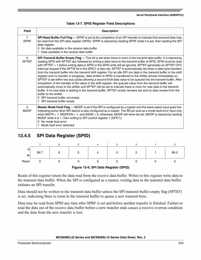
Serial Peripheral Interface (S08SPIV3)
MC9S08EL32 Series and MC9S08SL16 Series Data Sheet, Rev. 3
Freescale Semiconductor 243
13.4.5 SPI Data Register (SPID)
Reads of this register return the data read from the receive data buffer. Writes to this register write data to the transmit data buffer. When the SPI is configured as a master, writing data to the transmit data buffer initiates an SPI transfer.
Data should not be written to the transmit data buffer unless the SPI transmit buffer empty flag (SPTEF) is set, indicating there is room in the transmit buffer to queue a new transmit byte.
Data may be read from SPID any time after SPRF is set and before another transfer is finished. Failure to read the data out of the receive data buffer before a new transfer ends causes a receive overrun condition and the data from the new transfer is lost.
Table 13-7. SPIS Register Field Descriptions
Field Description
7SPRF
SPI Read Buffer Full Flag — SPRF is set at the completion of an SPI transfer to indicate that received data may be read from the SPI data register (SPID). SPRF is cleared by reading SPRF while it is set, then reading the SPI data register.0 No data available in the receive data buffer1 Data available in the receive data buffer
5SPTEF
SPI Transmit Buffer Empty Flag — This bit is set when there is room in the transmit data buffer. It is cleared by reading SPIS with SPTEF set, followed by writing a data value to the transmit buffer at SPID. SPIS must be read with SPTEF = 1 before writing data to SPID or the SPID write will be ignored. SPTEF generates an SPTEF CPU interrupt request if the SPTIE bit in the SPIC1 is also set. SPTEF is automatically set when a data byte transfers from the transmit buffer into the transmit shift register. For an idle SPI (no data in the transmit buffer or the shift register and no transfer in progress), data written to SPID is transferred to the shifter almost immediately so SPTEF is set within two bus cycles allowing a second 8-bit data value to be queued into the transmit buffer. After completion of the transfer of the value in the shift register, the queued value from the transmit buffer will automatically move to the shifter and SPTEF will be set to indicate there is room for new data in the transmit buffer. If no new data is waiting in the transmit buffer, SPTEF simply remains set and no data moves from the buffer to the shifter.0 SPI transmit buffer not empty1 SPI transmit buffer empty
4MODF
Master Mode Fault Flag — MODF is set if the SPI is configured as a master and the slave select input goes low, indicating some other SPI device is also configured as a master. The SS pin acts as a mode fault error input only when MSTR = 1, MODFEN = 1, and SSOE = 0; otherwise, MODF will never be set. MODF is cleared by reading MODF while it is 1, then writing to SPI control register 1 (SPIC1).0 No mode fault error1 Mode fault error detected
7 6 5 4 3 2 1 0
RBit 7 6 5 4 3 2 1 Bit 0
W
Reset 0 0 0 0 0 0 0 0
Figure 13-9. SPI Data Register (SPID)
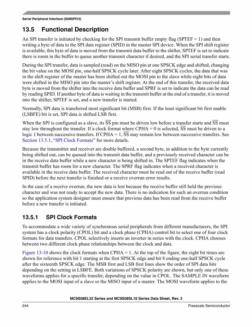
Serial Peripheral Interface (S08SPIV3)
MC9S08EL32 Series and MC9S08SL16 Series Data Sheet, Rev. 3
244 Freescale Semiconductor
13.5 Functional DescriptionAn SPI transfer is initiated by checking for the SPI transmit buffer empty flag (SPTEF = 1) and then writing a byte of data to the SPI data register (SPID) in the master SPI device. When the SPI shift register is available, this byte of data is moved from the transmit data buffer to the shifter, SPTEF is set to indicate there is room in the buffer to queue another transmit character if desired, and the SPI serial transfer starts.
During the SPI transfer, data is sampled (read) on the MISO pin at one SPSCK edge and shifted, changing the bit value on the MOSI pin, one-half SPSCK cycle later. After eight SPSCK cycles, the data that was in the shift register of the master has been shifted out the MOSI pin to the slave while eight bits of data were shifted in the MISO pin into the master’s shift register. At the end of this transfer, the received data byte is moved from the shifter into the receive data buffer and SPRF is set to indicate the data can be read by reading SPID. If another byte of data is waiting in the transmit buffer at the end of a transfer, it is moved into the shifter, SPTEF is set, and a new transfer is started.
Normally, SPI data is transferred most significant bit (MSB) first. If the least significant bit first enable (LSBFE) bit is set, SPI data is shifted LSB first.
When the SPI is configured as a slave, its SS pin must be driven low before a transfer starts and SS must stay low throughout the transfer. If a clock format where CPHA = 0 is selected, SS must be driven to a logic 1 between successive transfers. If CPHA = 1, SS may remain low between successive transfers. See Section 13.5.1, “SPI Clock Formats” for more details.
Because the transmitter and receiver are double buffered, a second byte, in addition to the byte currently being shifted out, can be queued into the transmit data buffer, and a previously received character can be in the receive data buffer while a new character is being shifted in. The SPTEF flag indicates when the transmit buffer has room for a new character. The SPRF flag indicates when a received character is available in the receive data buffer. The received character must be read out of the receive buffer (read SPID) before the next transfer is finished or a receive overrun error results.
In the case of a receive overrun, the new data is lost because the receive buffer still held the previous character and was not ready to accept the new data. There is no indication for such an overrun condition so the application system designer must ensure that previous data has been read from the receive buffer before a new transfer is initiated.
13.5.1 SPI Clock Formats
To accommodate a wide variety of synchronous serial peripherals from different manufacturers, the SPI system has a clock polarity (CPOL) bit and a clock phase (CPHA) control bit to select one of four clock formats for data transfers. CPOL selectively inserts an inverter in series with the clock. CPHA chooses between two different clock phase relationships between the clock and data.
Figure 13-10 shows the clock formats when CPHA = 1. At the top of the figure, the eight bit times are shown for reference with bit 1 starting at the first SPSCK edge and bit 8 ending one-half SPSCK cycle after the sixteenth SPSCK edge. The MSB first and LSB first lines show the order of SPI data bits depending on the setting in LSBFE. Both variations of SPSCK polarity are shown, but only one of these waveforms applies for a specific transfer, depending on the value in CPOL. The SAMPLE IN waveform applies to the MOSI input of a slave or the MISO input of a master. The MOSI waveform applies to the
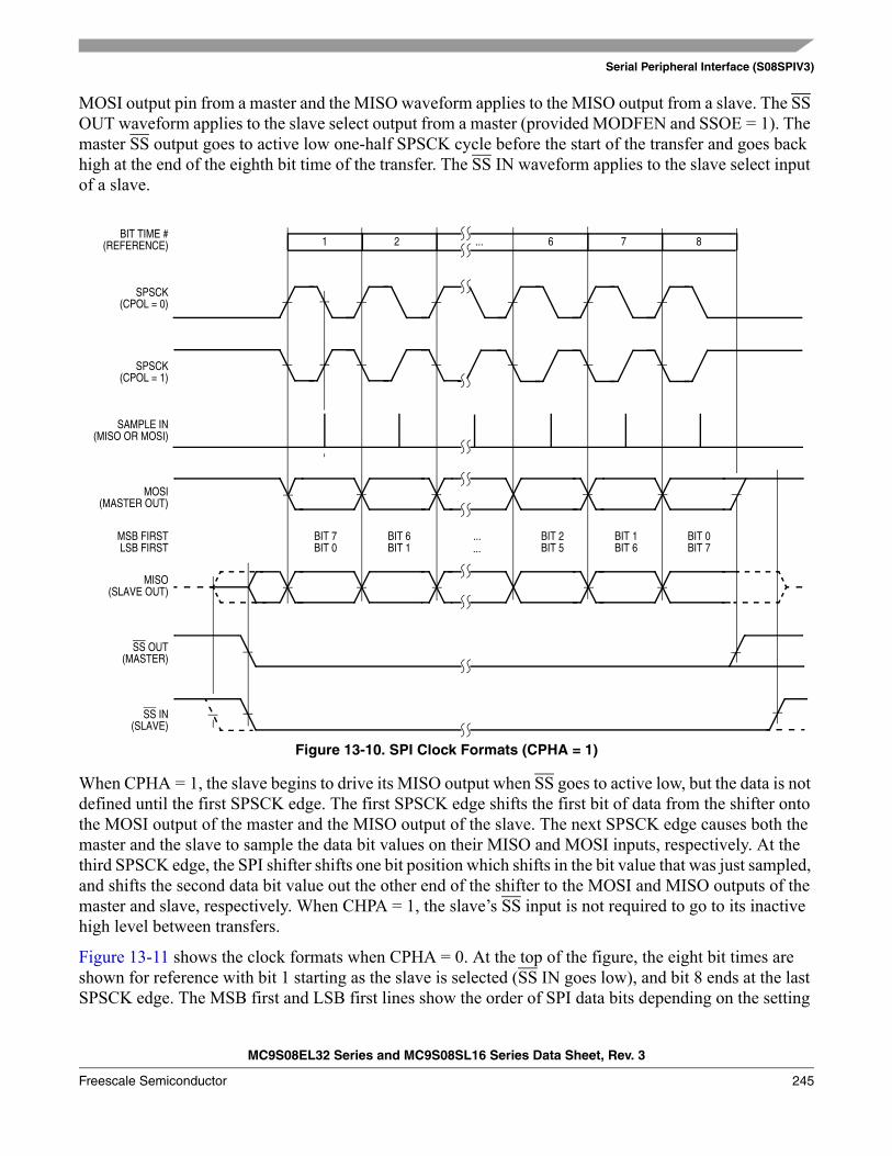
Serial Peripheral Interface (S08SPIV3)
MC9S08EL32 Series and MC9S08SL16 Series Data Sheet, Rev. 3
Freescale Semiconductor 245
MOSI output pin from a master and the MISO waveform applies to the MISO output from a slave. The SS OUT waveform applies to the slave select output from a master (provided MODFEN and SSOE = 1). The master SS output goes to active low one-half SPSCK cycle before the start of the transfer and goes back high at the end of the eighth bit time of the transfer. The SS IN waveform applies to the slave select input of a slave.
Figure 13-10. SPI Clock Formats (CPHA = 1)
When CPHA = 1, the slave begins to drive its MISO output when SS goes to active low, but the data is not defined until the first SPSCK edge. The first SPSCK edge shifts the first bit of data from the shifter onto the MOSI output of the master and the MISO output of the slave. The next SPSCK edge causes both the master and the slave to sample the data bit values on their MISO and MOSI inputs, respectively. At the third SPSCK edge, the SPI shifter shifts one bit position which shifts in the bit value that was just sampled, and shifts the second data bit value out the other end of the shifter to the MOSI and MISO outputs of the master and slave, respectively. When CHPA = 1, the slave’s SS input is not required to go to its inactive high level between transfers.
Figure 13-11 shows the clock formats when CPHA = 0. At the top of the figure, the eight bit times are shown for reference with bit 1 starting as the slave is selected (SS IN goes low), and bit 8 ends at the last SPSCK edge. The MSB first and LSB first lines show the order of SPI data bits depending on the setting
BIT TIME #(REFERENCE)
MSB FIRSTLSB FIRST
SPSCK(CPOL = 0)
SPSCK(CPOL = 1)
SAMPLE IN(MISO OR MOSI)
MOSI(MASTER OUT)
MISO(SLAVE OUT)
SS OUT(MASTER)
SS IN(SLAVE)
BIT 7BIT 0
BIT 6BIT 1
BIT 2BIT 5
BIT 1BIT 6
BIT 0BIT 7
1 2 6 7 8
...
...
...
Serial Peripheral Interface (S08SPIV3)
MC9S08EL32 Series and MC9S08SL16 Series Data Sheet, Rev. 3
246 Freescale Semiconductor
in LSBFE. Both variations of SPSCK polarity are shown, but only one of these waveforms applies for a specific transfer, depending on the value in CPOL. The SAMPLE IN waveform applies to the MOSI input of a slave or the MISO input of a master. The MOSI waveform applies to the MOSI output pin from a master and the MISO waveform applies to the MISO output from a slave. The SS OUT waveform applies to the slave select output from a master (provided MODFEN and SSOE = 1). The master SS output goes to active low at the start of the first bit time of the transfer and goes back high one-half SPSCK cycle after the end of the eighth bit time of the transfer. The SS IN waveform applies to the slave select input of a slave.
Figure 13-11. SPI Clock Formats (CPHA = 0)
When CPHA = 0, the slave begins to drive its MISO output with the first data bit value (MSB or LSB depending on LSBFE) when SS goes to active low. The first SPSCK edge causes both the master and the slave to sample the data bit values on their MISO and MOSI inputs, respectively. At the second SPSCK edge, the SPI shifter shifts one bit position which shifts in the bit value that was just sampled and shifts the second data bit value out the other end of the shifter to the MOSI and MISO outputs of the master and slave, respectively. When CPHA = 0, the slave’s SS input must go to its inactive high level between transfers.
BIT TIME #(REFERENCE)
MSB FIRSTLSB FIRST
SPSCK(CPOL = 0)
SPSCK(CPOL = 1)
SAMPLE IN(MISO OR MOSI)
MOSI(MASTER OUT)
MISO(SLAVE OUT)
SS OUT(MASTER)
SS IN(SLAVE)
BIT 7BIT 0
BIT 6BIT 1
BIT 2BIT 5
BIT 1BIT 6
BIT 0BIT 7
1 2 6 7 8...
...
...
Serial Peripheral Interface (S08SPIV3)
MC9S08EL32 Series and MC9S08SL16 Series Data Sheet, Rev. 3
Freescale Semiconductor 247
13.5.2 SPI Interrupts
There are three flag bits, two interrupt mask bits, and one interrupt vector associated with the SPI system. The SPI interrupt enable mask (SPIE) enables interrupts from the SPI receiver full flag (SPRF) and mode fault flag (MODF). The SPI transmit interrupt enable mask (SPTIE) enables interrupts from the SPI transmit buffer empty flag (SPTEF). When one of the flag bits is set, and the associated interrupt mask bit is set, a hardware interrupt request is sent to the CPU. If the interrupt mask bits are cleared, software can poll the associated flag bits instead of using interrupts. The SPI interrupt service routine (ISR) should check the flag bits to determine what event caused the interrupt. The service routine should also clear the flag bit(s) before returning from the ISR (usually near the beginning of the ISR).
13.5.3 Mode Fault Detection
A mode fault occurs and the mode fault flag (MODF) becomes set when a master SPI device detects an error on the SS pin (provided the SS pin is configured as the mode fault input signal). The SS pin is configured to be the mode fault input signal when MSTR = 1, mode fault enable is set (MODFEN = 1), and slave select output enable is clear (SSOE = 0).
The mode fault detection feature can be used in a system where more than one SPI device might become a master at the same time. The error is detected when a master’s SS pin is low, indicating that some other SPI device is trying to address this master as if it were a slave. This could indicate a harmful output driver conflict, so the mode fault logic is designed to disable all SPI output drivers when such an error is detected.
When a mode fault is detected, MODF is set and MSTR is cleared to change the SPI configuration back to slave mode. The output drivers on the SPSCK, MOSI, and MISO (if not bidirectional mode) are disabled.
MODF is cleared by reading it while it is set, then writing to the SPI control register 1 (SPIC1). User software should verify the error condition has been corrected before changing the SPI back to master mode.

Serial Peripheral Interface (S08SPIV3)
MC9S08EL32 Series and MC9S08SL16 Series Data Sheet, Rev. 3
248 Freescale Semiconductor
MC9S08EL32 Series and MC9S08SL16 Series Data Sheet, Rev. 3
Freescale Semiconductor 249
Chapter 14 Serial Communications Interface (S08SCIV4)
14.1 IntroductionThe MC9S08EL32 Series and MC9S08SL16 Series include a specially designed serial communications interface modules.
NOTEThe MC9S08EL32 Series and MC9S08SL16 Series Family of devices operates at a higher voltage range (2.7 V to 5.5 V) and does not include stop1 mode.
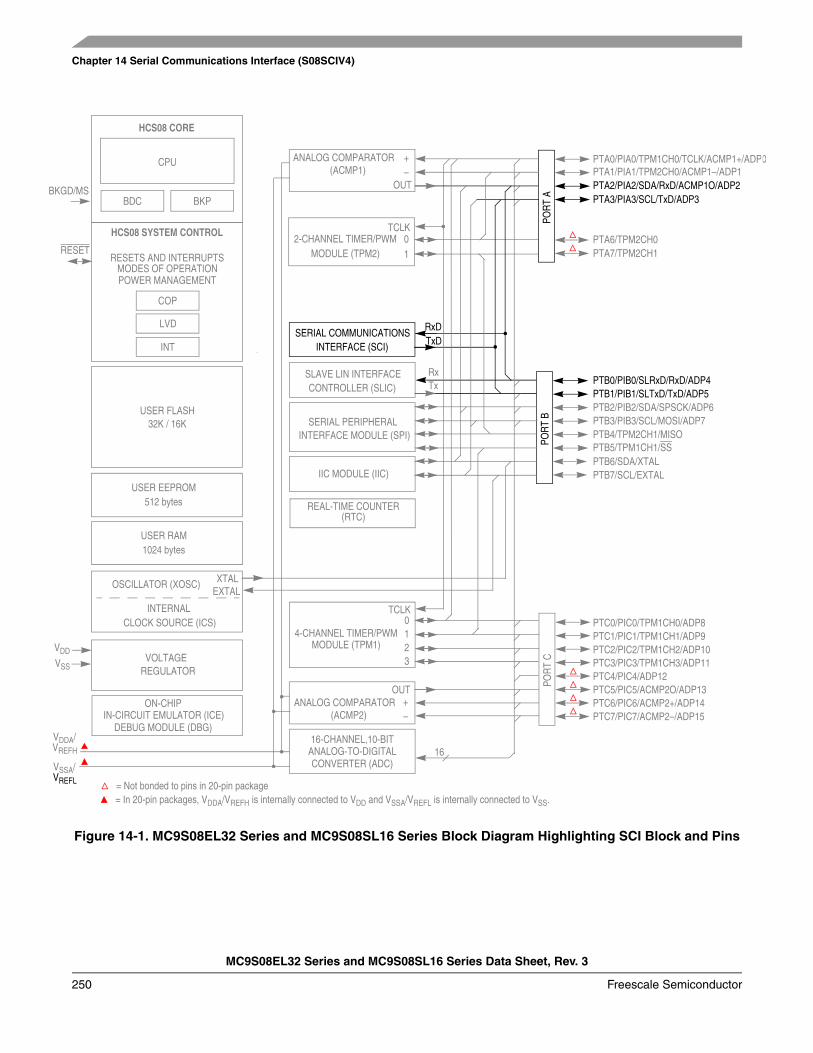
Chapter 14 Serial Communications Interface (S08SCIV4)
MC9S08EL32 Series and MC9S08SL16 Series Data Sheet, Rev. 3
250 Freescale Semiconductor
Figure 14-1. MC9S08EL32 Series and MC9S08SL16 Series Block Diagram Highlighting SCI Block and Pins
VSS
IIC MODULE (IIC)
SERIAL PERIPHERAL INTERFACE MODULE (SPI)
USER FLASH
USER RAM
32K / 16K
HCS08 CORE
CPU
BDC
2-CHANNEL TIMER/PWMMODULE (TPM2)
HCS08 SYSTEM CONTROL
RESETS AND INTERRUPTSMODES OF OPERATIONPOWER MANAGEMENT
VOLTAGE REGULATOR
COP
LVD
OSCILLATOR (XOSC)
INTERNALCLOCK SOURCE (ICS)
RESET
VREFH
1024 bytes
INTERFACE (SCI)SERIAL COMMUNICATIONS
XTALEXTAL
4-CHANNEL TIMER/PWMMODULE (TPM1)
REAL-TIME COUNTER
IN-CIRCUIT EMULATOR (ICE)
BKGD/MS PTA3/PIA3/SCL/TxD/ADP3
PTA6/TPM2CH0
PTA2/PIA2/SDA/RxD/ACMP1O/ADP2PTA1/PIA1/TPM2CH0/ACMP1–/ADP1PTA0/PIA0/TPM1CH0/TCLK/ACMP1+/ADP0
PTA7/TPM2CH1
PTB3/PIB3/SCL/MOSI/ADP7PTB4/TPM2CH1/MISO
PTB2/PIB2/SDA/SPSCK/ADP6PTB1/PIB1/SLTxD/TxD/ADP5PTB0/PIB0/SLRxD/RxD/ADP4
PTB7/SCL/EXTAL
PTC3/PIC3/TPM1CH3/ADP11PTC4/PIC4/ADP12PTC5/PIC5/ACMP2O/ADP13
PTC2/PIC2/TPM1CH2/ADP10PTC1/PIC1/TPM1CH1/ADP9
POR
T C
PTC6/PIC6/ACMP2+/ADP14
VDD
BKP
INT
ANALOG COMPARATOR(ACMP2)
USER EEPROM512 bytes
CONTROLLER (SLIC)SLAVE LIN INTERFACE
ANALOG-TO-DIGITALCONVERTER (ADC)
16-CHANNEL,10-BIT16
= In 20-pin packages, VDDA/VREFH is internally connected to VDD and VSSA/VREFL is internally connected to VSS.
VDDA/
VREFL
VSSA/
DEBUG MODULE (DBG)
ON-CHIP
(RTC)
PTC0/PIC0/TPM1CH0/ADP8
PTC7/PIC7/ACMP2–/ADP15
PTB6/SDA/XTAL
POR
T B
POR
T A
PTB5/TPM1CH1/SS
ANALOG COMPARATOR(ACMP1)
= Not bonded to pins in 20-pin package
TCLK
TCLK
+–
OUT
+–
OUT
0123
10
RxDTxD
TxRx
Serial Communications Interface (S08SCIV4)
MC9S08EL32 Series and MC9S08SL16 Series Data Sheet, Rev. 3
Freescale Semiconductor 251
14.1.1 Features
Features of SCI module include:• Full-duplex, standard non-return-to-zero (NRZ) format• Double-buffered transmitter and receiver with separate enables• Programmable baud rates (13-bit modulo divider)• Interrupt-driven or polled operation:
— Transmit data register empty and transmission complete— Receive data register full— Receive overrun, parity error, framing error, and noise error— Idle receiver detect— Active edge on receive pin— Break detect supporting LIN
• Hardware parity generation and checking• Programmable 8-bit or 9-bit character length• Receiver wakeup by idle-line or address-mark• Optional 13-bit break character generation / 11-bit break character detection• Selectable transmitter output polarity
14.1.2 Modes of Operation
See Section 14.3, “Functional Description,” For details concerning SCI operation in these modes:• 8- and 9-bit data modes• Stop mode operation• Loop mode• Single-wire mode
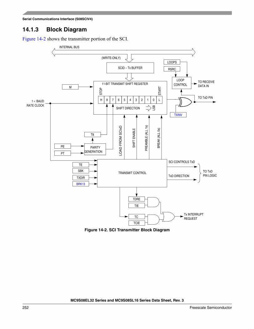
Serial Communications Interface (S08SCIV4)
MC9S08EL32 Series and MC9S08SL16 Series Data Sheet, Rev. 3
252 Freescale Semiconductor
14.1.3 Block Diagram
Figure 14-2 shows the transmitter portion of the SCI.
Figure 14-2. SCI Transmitter Block Diagram
H 8 7 6 5 4 3 2 1 0 L
SCID – Tx BUFFER
(WRITE-ONLY)
INTERNAL BUS
STO
P
11-BIT TRANSMIT SHIFT REGISTER
STAR
T
SHIFT DIRECTION LSB
1 × BAUDRATE CLOCK
PARITYGENERATION
TRANSMIT CONTROL
SHIF
T EN
ABLE
PREA
MBL
E (A
LL 1
s)
BREA
K (A
LL 0
s)SCI CONTROLS TxD
TxD DIRECTIONTO TxDPIN LOGIC
LOOPCONTROL
TO RECEIVEDATA IN
TO TxD PIN
Tx INTERRUPTREQUEST
LOOPS
RSRC
TIE
TC
TDRE
M
PT
PE
TCIE
TE
SBK
T8
TXDIR
LOA
D F
RO
M S
CIx
D
TXINV
BRK13
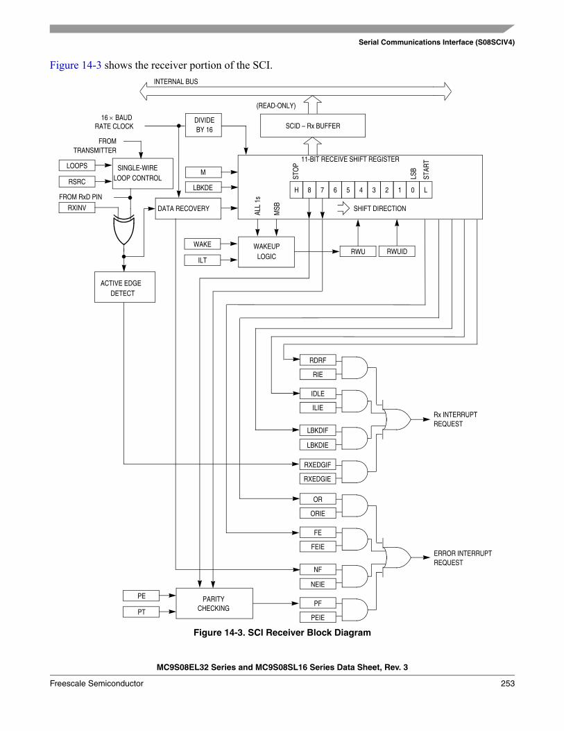
Serial Communications Interface (S08SCIV4)
MC9S08EL32 Series and MC9S08SL16 Series Data Sheet, Rev. 3
Freescale Semiconductor 253
Figure 14-3 shows the receiver portion of the SCI.
Figure 14-3. SCI Receiver Block Diagram
H 8 7 6 5 4 3 2 1 0 L
SCID – Rx BUFFER
(READ-ONLY)
INTERNAL BUS
STO
P
11-BIT RECEIVE SHIFT REGISTER
STAR
T
SHIFT DIRECTION
LSB
FROM RxD PIN
RATE CLOCK
Rx INTERRUPTREQUEST
DATA RECOVERY
DIVIDE16 × BAUD
SINGLE-WIRELOOP CONTROL
WAKEUPLOGIC
ALL
1s
MSB
FROMTRANSMITTER
ERROR INTERRUPTREQUEST
PARITYCHECKING
BY 16
RDRF
RIE
IDLE
ILIE
OR
ORIE
FE
FEIE
NF
NEIE
PF
LOOPS
PEIEPT
PE
RSRC
WAKE
ILTRWU
M
LBKDIF
LBKDIE
RXEDGIF
RXEDGIE
ACTIVE EDGEDETECT
RXINV
LBKDE
RWUID
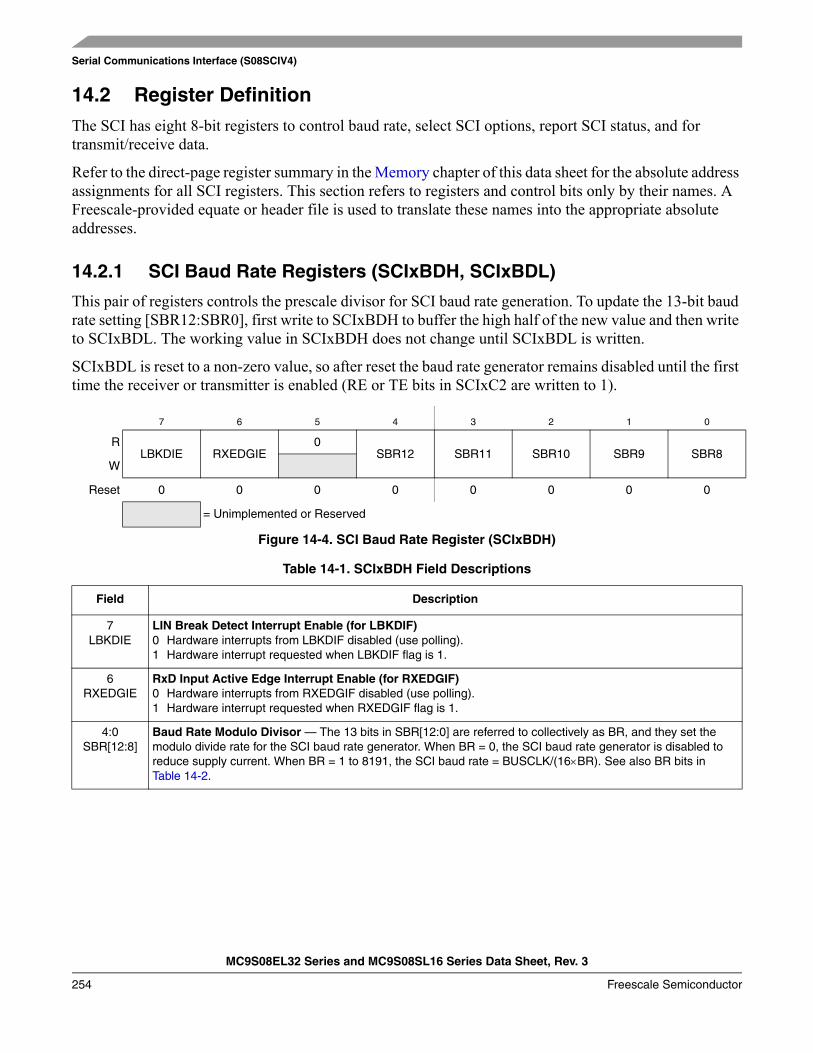
Serial Communications Interface (S08SCIV4)
MC9S08EL32 Series and MC9S08SL16 Series Data Sheet, Rev. 3
254 Freescale Semiconductor
14.2 Register DefinitionThe SCI has eight 8-bit registers to control baud rate, select SCI options, report SCI status, and for transmit/receive data.
Refer to the direct-page register summary in the Memory chapter of this data sheet for the absolute address assignments for all SCI registers. This section refers to registers and control bits only by their names. A Freescale-provided equate or header file is used to translate these names into the appropriate absolute addresses.
14.2.1 SCI Baud Rate Registers (SCIxBDH, SCIxBDL)
This pair of registers controls the prescale divisor for SCI baud rate generation. To update the 13-bit baud rate setting [SBR12:SBR0], first write to SCIxBDH to buffer the high half of the new value and then write to SCIxBDL. The working value in SCIxBDH does not change until SCIxBDL is written.
SCIxBDL is reset to a non-zero value, so after reset the baud rate generator remains disabled until the first time the receiver or transmitter is enabled (RE or TE bits in SCIxC2 are written to 1).
7 6 5 4 3 2 1 0
RLBKDIE RXEDGIE
0SBR12 SBR11 SBR10 SBR9 SBR8
W
Reset 0 0 0 0 0 0 0 0
= Unimplemented or Reserved
Figure 14-4. SCI Baud Rate Register (SCIxBDH)
Table 14-1. SCIxBDH Field Descriptions
Field Description
7LBKDIE
LIN Break Detect Interrupt Enable (for LBKDIF)0 Hardware interrupts from LBKDIF disabled (use polling).1 Hardware interrupt requested when LBKDIF flag is 1.
6RXEDGIE
RxD Input Active Edge Interrupt Enable (for RXEDGIF)0 Hardware interrupts from RXEDGIF disabled (use polling).1 Hardware interrupt requested when RXEDGIF flag is 1.
4:0SBR[12:8]
Baud Rate Modulo Divisor — The 13 bits in SBR[12:0] are referred to collectively as BR, and they set the modulo divide rate for the SCI baud rate generator. When BR = 0, the SCI baud rate generator is disabled to reduce supply current. When BR = 1 to 8191, the SCI baud rate = BUSCLK/(16×BR). See also BR bits in Table 14-2.
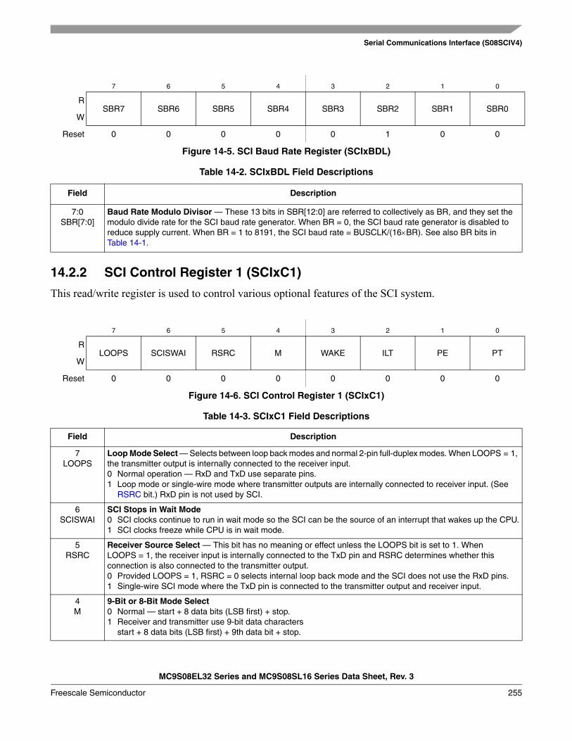
Serial Communications Interface (S08SCIV4)
MC9S08EL32 Series and MC9S08SL16 Series Data Sheet, Rev. 3
Freescale Semiconductor 255
14.2.2 SCI Control Register 1 (SCIxC1)
This read/write register is used to control various optional features of the SCI system.
7 6 5 4 3 2 1 0
RSBR7 SBR6 SBR5 SBR4 SBR3 SBR2 SBR1 SBR0
W
Reset 0 0 0 0 0 1 0 0
Figure 14-5. SCI Baud Rate Register (SCIxBDL)
Table 14-2. SCIxBDL Field Descriptions
Field Description
7:0SBR[7:0]
Baud Rate Modulo Divisor — These 13 bits in SBR[12:0] are referred to collectively as BR, and they set the modulo divide rate for the SCI baud rate generator. When BR = 0, the SCI baud rate generator is disabled to reduce supply current. When BR = 1 to 8191, the SCI baud rate = BUSCLK/(16×BR). See also BR bits in Table 14-1.
7 6 5 4 3 2 1 0
RLOOPS SCISWAI RSRC M WAKE ILT PE PT
W
Reset 0 0 0 0 0 0 0 0
Figure 14-6. SCI Control Register 1 (SCIxC1)
Table 14-3. SCIxC1 Field Descriptions
Field Description
7LOOPS
Loop Mode Select — Selects between loop back modes and normal 2-pin full-duplex modes. When LOOPS = 1, the transmitter output is internally connected to the receiver input.0 Normal operation — RxD and TxD use separate pins.1 Loop mode or single-wire mode where transmitter outputs are internally connected to receiver input. (See
RSRC bit.) RxD pin is not used by SCI.
6SCISWAI
SCI Stops in Wait Mode0 SCI clocks continue to run in wait mode so the SCI can be the source of an interrupt that wakes up the CPU.1 SCI clocks freeze while CPU is in wait mode.
5RSRC
Receiver Source Select — This bit has no meaning or effect unless the LOOPS bit is set to 1. When LOOPS = 1, the receiver input is internally connected to the TxD pin and RSRC determines whether this connection is also connected to the transmitter output.0 Provided LOOPS = 1, RSRC = 0 selects internal loop back mode and the SCI does not use the RxD pins.1 Single-wire SCI mode where the TxD pin is connected to the transmitter output and receiver input.
4M
9-Bit or 8-Bit Mode Select0 Normal — start + 8 data bits (LSB first) + stop.1 Receiver and transmitter use 9-bit data characters
start + 8 data bits (LSB first) + 9th data bit + stop.
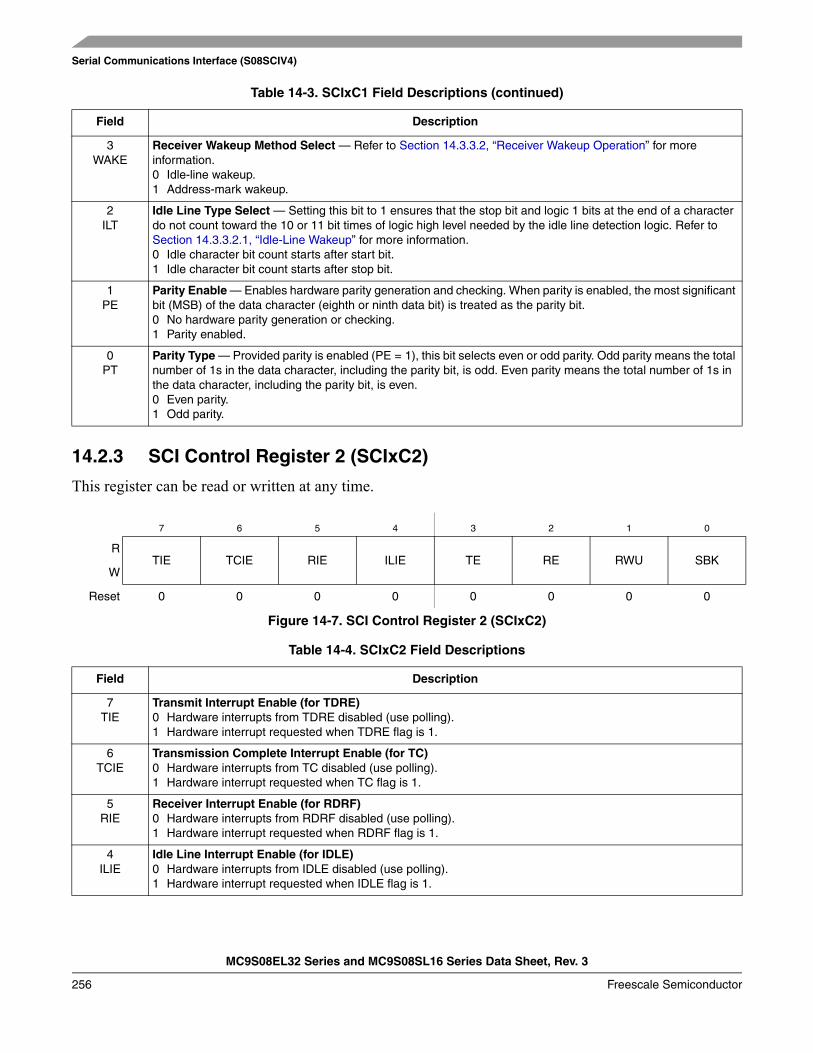
Serial Communications Interface (S08SCIV4)
MC9S08EL32 Series and MC9S08SL16 Series Data Sheet, Rev. 3
256 Freescale Semiconductor
14.2.3 SCI Control Register 2 (SCIxC2)
This register can be read or written at any time.
3WAKE
Receiver Wakeup Method Select — Refer to Section 14.3.3.2, “Receiver Wakeup Operation” for more information.0 Idle-line wakeup.1 Address-mark wakeup.
2ILT
Idle Line Type Select — Setting this bit to 1 ensures that the stop bit and logic 1 bits at the end of a character do not count toward the 10 or 11 bit times of logic high level needed by the idle line detection logic. Refer to Section 14.3.3.2.1, “Idle-Line Wakeup” for more information.0 Idle character bit count starts after start bit.1 Idle character bit count starts after stop bit.
1PE
Parity Enable — Enables hardware parity generation and checking. When parity is enabled, the most significant bit (MSB) of the data character (eighth or ninth data bit) is treated as the parity bit.0 No hardware parity generation or checking.1 Parity enabled.
0PT
Parity Type — Provided parity is enabled (PE = 1), this bit selects even or odd parity. Odd parity means the total number of 1s in the data character, including the parity bit, is odd. Even parity means the total number of 1s in the data character, including the parity bit, is even.0 Even parity.1 Odd parity.
7 6 5 4 3 2 1 0
RTIE TCIE RIE ILIE TE RE RWU SBK
W
Reset 0 0 0 0 0 0 0 0
Figure 14-7. SCI Control Register 2 (SCIxC2)
Table 14-4. SCIxC2 Field Descriptions
Field Description
7TIE
Transmit Interrupt Enable (for TDRE)0 Hardware interrupts from TDRE disabled (use polling).1 Hardware interrupt requested when TDRE flag is 1.
6TCIE
Transmission Complete Interrupt Enable (for TC)0 Hardware interrupts from TC disabled (use polling).1 Hardware interrupt requested when TC flag is 1.
5RIE
Receiver Interrupt Enable (for RDRF)0 Hardware interrupts from RDRF disabled (use polling).1 Hardware interrupt requested when RDRF flag is 1.
4ILIE
Idle Line Interrupt Enable (for IDLE)0 Hardware interrupts from IDLE disabled (use polling).1 Hardware interrupt requested when IDLE flag is 1.
Table 14-3. SCIxC1 Field Descriptions (continued)
Field Description
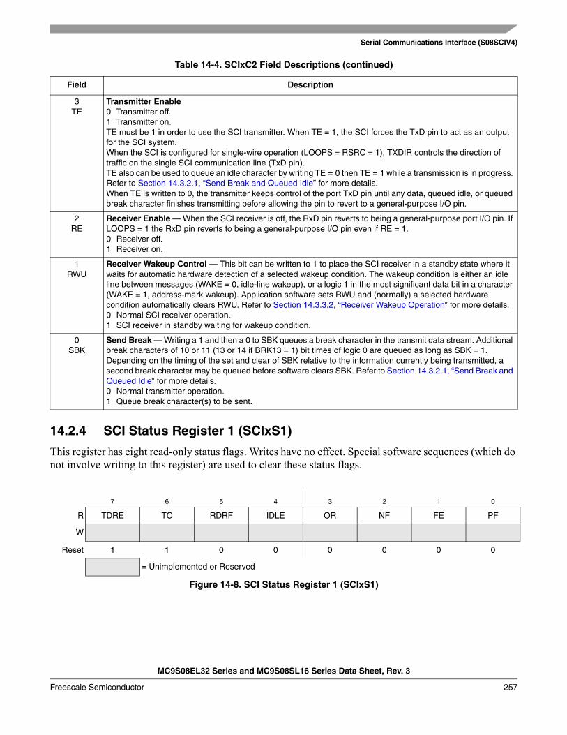
Serial Communications Interface (S08SCIV4)
MC9S08EL32 Series and MC9S08SL16 Series Data Sheet, Rev. 3
Freescale Semiconductor 257
14.2.4 SCI Status Register 1 (SCIxS1)
This register has eight read-only status flags. Writes have no effect. Special software sequences (which do not involve writing to this register) are used to clear these status flags.
3TE
Transmitter Enable0 Transmitter off.1 Transmitter on.TE must be 1 in order to use the SCI transmitter. When TE = 1, the SCI forces the TxD pin to act as an output for the SCI system.When the SCI is configured for single-wire operation (LOOPS = RSRC = 1), TXDIR controls the direction of traffic on the single SCI communication line (TxD pin).TE also can be used to queue an idle character by writing TE = 0 then TE = 1 while a transmission is in progress. Refer to Section 14.3.2.1, “Send Break and Queued Idle” for more details.When TE is written to 0, the transmitter keeps control of the port TxD pin until any data, queued idle, or queued break character finishes transmitting before allowing the pin to revert to a general-purpose I/O pin.
2RE
Receiver Enable — When the SCI receiver is off, the RxD pin reverts to being a general-purpose port I/O pin. If LOOPS = 1 the RxD pin reverts to being a general-purpose I/O pin even if RE = 1.0 Receiver off.1 Receiver on.
1RWU
Receiver Wakeup Control — This bit can be written to 1 to place the SCI receiver in a standby state where it waits for automatic hardware detection of a selected wakeup condition. The wakeup condition is either an idle line between messages (WAKE = 0, idle-line wakeup), or a logic 1 in the most significant data bit in a character (WAKE = 1, address-mark wakeup). Application software sets RWU and (normally) a selected hardware condition automatically clears RWU. Refer to Section 14.3.3.2, “Receiver Wakeup Operation” for more details.0 Normal SCI receiver operation.1 SCI receiver in standby waiting for wakeup condition.
0SBK
Send Break — Writing a 1 and then a 0 to SBK queues a break character in the transmit data stream. Additional break characters of 10 or 11 (13 or 14 if BRK13 = 1) bit times of logic 0 are queued as long as SBK = 1. Depending on the timing of the set and clear of SBK relative to the information currently being transmitted, a second break character may be queued before software clears SBK. Refer to Section 14.3.2.1, “Send Break and Queued Idle” for more details.0 Normal transmitter operation.1 Queue break character(s) to be sent.
7 6 5 4 3 2 1 0
R TDRE TC RDRF IDLE OR NF FE PF
W
Reset 1 1 0 0 0 0 0 0
= Unimplemented or Reserved
Figure 14-8. SCI Status Register 1 (SCIxS1)
Table 14-4. SCIxC2 Field Descriptions (continued)
Field Description
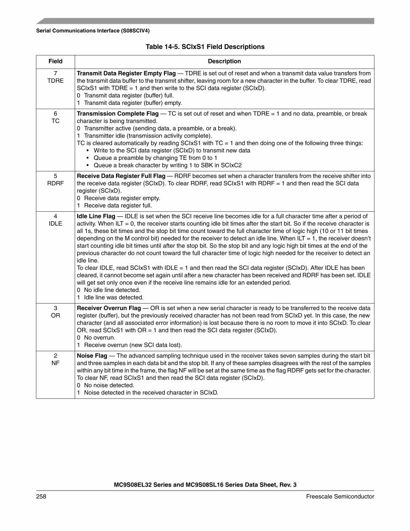
Serial Communications Interface (S08SCIV4)
MC9S08EL32 Series and MC9S08SL16 Series Data Sheet, Rev. 3
258 Freescale Semiconductor
Table 14-5. SCIxS1 Field Descriptions
Field Description
7TDRE
Transmit Data Register Empty Flag — TDRE is set out of reset and when a transmit data value transfers from the transmit data buffer to the transmit shifter, leaving room for a new character in the buffer. To clear TDRE, read SCIxS1 with TDRE = 1 and then write to the SCI data register (SCIxD).0 Transmit data register (buffer) full.1 Transmit data register (buffer) empty.
6TC
Transmission Complete Flag — TC is set out of reset and when TDRE = 1 and no data, preamble, or break character is being transmitted. 0 Transmitter active (sending data, a preamble, or a break).1 Transmitter idle (transmission activity complete).TC is cleared automatically by reading SCIxS1 with TC = 1 and then doing one of the following three things:
• Write to the SCI data register (SCIxD) to transmit new data• Queue a preamble by changing TE from 0 to 1• Queue a break character by writing 1 to SBK in SCIxC2
5RDRF
Receive Data Register Full Flag — RDRF becomes set when a character transfers from the receive shifter into the receive data register (SCIxD). To clear RDRF, read SCIxS1 with RDRF = 1 and then read the SCI data register (SCIxD).0 Receive data register empty.1 Receive data register full.
4IDLE
Idle Line Flag — IDLE is set when the SCI receive line becomes idle for a full character time after a period of activity. When ILT = 0, the receiver starts counting idle bit times after the start bit. So if the receive character is all 1s, these bit times and the stop bit time count toward the full character time of logic high (10 or 11 bit times depending on the M control bit) needed for the receiver to detect an idle line. When ILT = 1, the receiver doesn’t start counting idle bit times until after the stop bit. So the stop bit and any logic high bit times at the end of the previous character do not count toward the full character time of logic high needed for the receiver to detect an idle line.To clear IDLE, read SCIxS1 with IDLE = 1 and then read the SCI data register (SCIxD). After IDLE has been cleared, it cannot become set again until after a new character has been received and RDRF has been set. IDLE will get set only once even if the receive line remains idle for an extended period.0 No idle line detected.1 Idle line was detected.
3OR
Receiver Overrun Flag — OR is set when a new serial character is ready to be transferred to the receive data register (buffer), but the previously received character has not been read from SCIxD yet. In this case, the new character (and all associated error information) is lost because there is no room to move it into SCIxD. To clear OR, read SCIxS1 with OR = 1 and then read the SCI data register (SCIxD).0 No overrun.1 Receive overrun (new SCI data lost).
2NF
Noise Flag — The advanced sampling technique used in the receiver takes seven samples during the start bit and three samples in each data bit and the stop bit. If any of these samples disagrees with the rest of the samples within any bit time in the frame, the flag NF will be set at the same time as the flag RDRF gets set for the character. To clear NF, read SCIxS1 and then read the SCI data register (SCIxD).0 No noise detected.1 Noise detected in the received character in SCIxD.
Serial Communications Interface (S08SCIV4)
MC9S08EL32 Series and MC9S08SL16 Series Data Sheet, Rev. 3
Freescale Semiconductor 259
14.2.5 SCI Status Register 2 (SCIxS2)
This register has one read-only status flag.
1FE
Framing Error Flag — FE is set at the same time as RDRF when the receiver detects a logic 0 where the stop bit was expected. This suggests the receiver was not properly aligned to a character frame. To clear FE, read SCIxS1 with FE = 1 and then read the SCI data register (SCIxD).0 No framing error detected. This does not guarantee the framing is correct.1 Framing error.
0PF
Parity Error Flag — PF is set at the same time as RDRF when parity is enabled (PE = 1) and the parity bit in the received character does not agree with the expected parity value. To clear PF, read SCIxS1 and then read the SCI data register (SCIxD).0 No parity error. 1 Parity error.
7 6 5 4 3 2 1 0
RLBKDIF RXEDGIF
0RXINV RWUID BRK13 LBKDE
RAF
W
Reset 0 0 0 0 0 0 0 0
= Unimplemented or Reserved
Figure 14-9. SCI Status Register 2 (SCIxS2)
Table 14-6. SCIxS2 Field Descriptions
Field Description
7LBKDIF
LIN Break Detect Interrupt Flag — LBKDIF is set when the LIN break detect circuitry is enabled and a LIN break character is detected. LBKDIF is cleared by writing a “1” to it.0 No LIN break character has been detected.1 LIN break character has been detected.
6RXEDGIF
RxD Pin Active Edge Interrupt Flag — RXEDGIF is set when an active edge (falling if RXINV = 0, rising if RXINV=1) on the RxD pin occurs. RXEDGIF is cleared by writing a “1” to it.0 No active edge on the receive pin has occurred.1 An active edge on the receive pin has occurred.
4RXINV1
Receive Data Inversion — Setting this bit reverses the polarity of the received data input.0 Receive data not inverted1 Receive data inverted
3RWUID
Receive Wake Up Idle Detect— RWUID controls whether the idle character that wakes up the receiver sets the IDLE bit.0 During receive standby state (RWU = 1), the IDLE bit does not get set upon detection of an idle character.1 During receive standby state (RWU = 1), the IDLE bit gets set upon detection of an idle character.
2BRK13
Break Character Generation Length — BRK13 is used to select a longer transmitted break character length. Detection of a framing error is not affected by the state of this bit.0 Break character is transmitted with length of 10 bit times (11 if M = 1)1 Break character is transmitted with length of 13 bit times (14 if M = 1)
Table 14-5. SCIxS1 Field Descriptions (continued)
Field Description
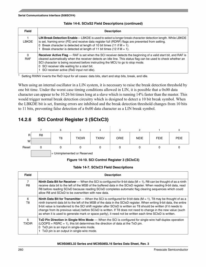
Serial Communications Interface (S08SCIV4)
MC9S08EL32 Series and MC9S08SL16 Series Data Sheet, Rev. 3
260 Freescale Semiconductor
When using an internal oscillator in a LIN system, it is necessary to raise the break detection threshold by one bit time. Under the worst case timing conditions allowed in LIN, it is possible that a 0x00 data character can appear to be 10.26 bit times long at a slave which is running 14% faster than the master. This would trigger normal break detection circuitry which is designed to detect a 10 bit break symbol. When the LBKDE bit is set, framing errors are inhibited and the break detection threshold changes from 10 bits to 11 bits, preventing false detection of a 0x00 data character as a LIN break symbol.
14.2.6 SCI Control Register 3 (SCIxC3)
1LBKDE
LIN Break Detection Enable— LBKDE is used to select a longer break character detection length. While LBKDE is set, framing error (FE) and receive data register full (RDRF) flags are prevented from setting.0 Break character is detected at length of 10 bit times (11 if M = 1).1 Break character is detected at length of 11 bit times (12 if M = 1).
0RAF
Receiver Active Flag — RAF is set when the SCI receiver detects the beginning of a valid start bit, and RAF is cleared automatically when the receiver detects an idle line. This status flag can be used to check whether an SCI character is being received before instructing the MCU to go to stop mode.0 SCI receiver idle waiting for a start bit.1 SCI receiver active (RxD input not idle).
1 Setting RXINV inverts the RxD input for all cases: data bits, start and stop bits, break, and idle.
7 6 5 4 3 2 1 0
R R8T8 TXDIR TXINV ORIE NEIE FEIE PEIE
W
Reset 0 0 0 0 0 0 0 0
= Unimplemented or Reserved
Figure 14-10. SCI Control Register 3 (SCIxC3)
Table 14-7. SCIxC3 Field Descriptions
Field Description
7R8
Ninth Data Bit for Receiver — When the SCI is configured for 9-bit data (M = 1), R8 can be thought of as a ninth receive data bit to the left of the MSB of the buffered data in the SCIxD register. When reading 9-bit data, read R8 before reading SCIxD because reading SCIxD completes automatic flag clearing sequences which could allow R8 and SCIxD to be overwritten with new data.
6T8
Ninth Data Bit for Transmitter — When the SCI is configured for 9-bit data (M = 1), T8 may be thought of as a ninth transmit data bit to the left of the MSB of the data in the SCIxD register. When writing 9-bit data, the entire 9-bit value is transferred to the SCI shift register after SCIxD is written so T8 should be written (if it needs to change from its previous value) before SCIxD is written. If T8 does not need to change in the new value (such as when it is used to generate mark or space parity), it need not be written each time SCIxD is written.
5TXDIR
TxD Pin Direction in Single-Wire Mode — When the SCI is configured for single-wire half-duplex operation (LOOPS = RSRC = 1), this bit determines the direction of data at the TxD pin.0 TxD pin is an input in single-wire mode.1 TxD pin is an output in single-wire mode.
Table 14-6. SCIxS2 Field Descriptions (continued)
Field Description
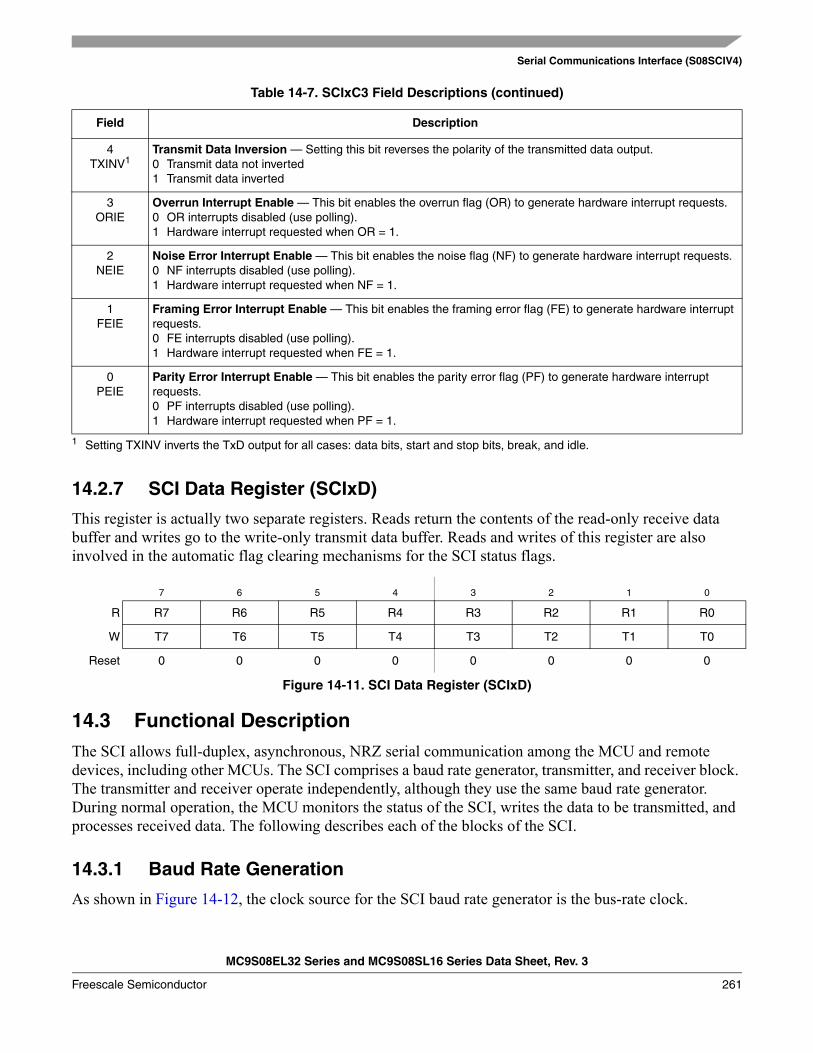
Serial Communications Interface (S08SCIV4)
MC9S08EL32 Series and MC9S08SL16 Series Data Sheet, Rev. 3
Freescale Semiconductor 261
14.2.7 SCI Data Register (SCIxD)
This register is actually two separate registers. Reads return the contents of the read-only receive data buffer and writes go to the write-only transmit data buffer. Reads and writes of this register are also involved in the automatic flag clearing mechanisms for the SCI status flags.
14.3 Functional DescriptionThe SCI allows full-duplex, asynchronous, NRZ serial communication among the MCU and remote devices, including other MCUs. The SCI comprises a baud rate generator, transmitter, and receiver block. The transmitter and receiver operate independently, although they use the same baud rate generator. During normal operation, the MCU monitors the status of the SCI, writes the data to be transmitted, and processes received data. The following describes each of the blocks of the SCI.
14.3.1 Baud Rate Generation
As shown in Figure 14-12, the clock source for the SCI baud rate generator is the bus-rate clock.
4TXINV1
Transmit Data Inversion — Setting this bit reverses the polarity of the transmitted data output.0 Transmit data not inverted1 Transmit data inverted
3ORIE
Overrun Interrupt Enable — This bit enables the overrun flag (OR) to generate hardware interrupt requests.0 OR interrupts disabled (use polling).1 Hardware interrupt requested when OR = 1.
2NEIE
Noise Error Interrupt Enable — This bit enables the noise flag (NF) to generate hardware interrupt requests.0 NF interrupts disabled (use polling).1 Hardware interrupt requested when NF = 1.
1FEIE
Framing Error Interrupt Enable — This bit enables the framing error flag (FE) to generate hardware interrupt requests.0 FE interrupts disabled (use polling).1 Hardware interrupt requested when FE = 1.
0PEIE
Parity Error Interrupt Enable — This bit enables the parity error flag (PF) to generate hardware interrupt requests.0 PF interrupts disabled (use polling).1 Hardware interrupt requested when PF = 1.
1 Setting TXINV inverts the TxD output for all cases: data bits, start and stop bits, break, and idle.
7 6 5 4 3 2 1 0
R R7 R6 R5 R4 R3 R2 R1 R0
W T7 T6 T5 T4 T3 T2 T1 T0
Reset 0 0 0 0 0 0 0 0
Figure 14-11. SCI Data Register (SCIxD)
Table 14-7. SCIxC3 Field Descriptions (continued)
Field Description
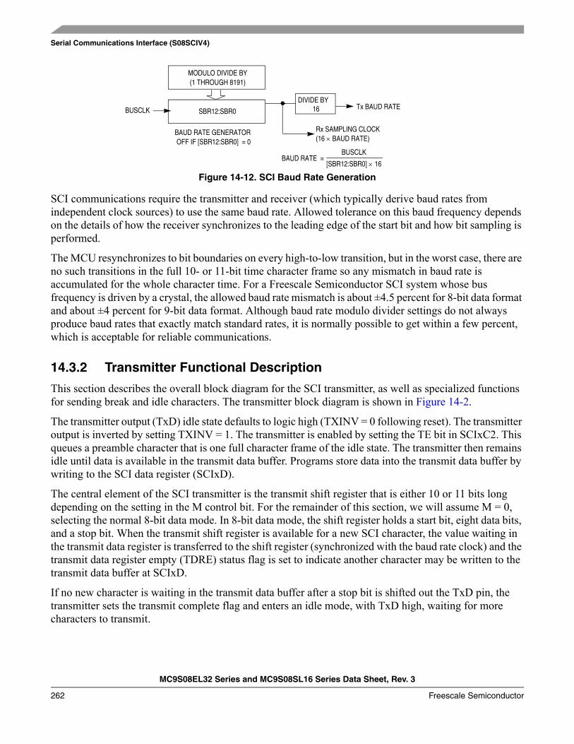
Serial Communications Interface (S08SCIV4)
MC9S08EL32 Series and MC9S08SL16 Series Data Sheet, Rev. 3
262 Freescale Semiconductor
Figure 14-12. SCI Baud Rate Generation
SCI communications require the transmitter and receiver (which typically derive baud rates from independent clock sources) to use the same baud rate. Allowed tolerance on this baud frequency depends on the details of how the receiver synchronizes to the leading edge of the start bit and how bit sampling is performed.
The MCU resynchronizes to bit boundaries on every high-to-low transition, but in the worst case, there are no such transitions in the full 10- or 11-bit time character frame so any mismatch in baud rate is accumulated for the whole character time. For a Freescale Semiconductor SCI system whose bus frequency is driven by a crystal, the allowed baud rate mismatch is about ±4.5 percent for 8-bit data format and about ±4 percent for 9-bit data format. Although baud rate modulo divider settings do not always produce baud rates that exactly match standard rates, it is normally possible to get within a few percent, which is acceptable for reliable communications.
14.3.2 Transmitter Functional Description
This section describes the overall block diagram for the SCI transmitter, as well as specialized functions for sending break and idle characters. The transmitter block diagram is shown in Figure 14-2.
The transmitter output (TxD) idle state defaults to logic high (TXINV = 0 following reset). The transmitter output is inverted by setting TXINV = 1. The transmitter is enabled by setting the TE bit in SCIxC2. This queues a preamble character that is one full character frame of the idle state. The transmitter then remains idle until data is available in the transmit data buffer. Programs store data into the transmit data buffer by writing to the SCI data register (SCIxD).
The central element of the SCI transmitter is the transmit shift register that is either 10 or 11 bits long depending on the setting in the M control bit. For the remainder of this section, we will assume M = 0, selecting the normal 8-bit data mode. In 8-bit data mode, the shift register holds a start bit, eight data bits, and a stop bit. When the transmit shift register is available for a new SCI character, the value waiting in the transmit data register is transferred to the shift register (synchronized with the baud rate clock) and the transmit data register empty (TDRE) status flag is set to indicate another character may be written to the transmit data buffer at SCIxD.
If no new character is waiting in the transmit data buffer after a stop bit is shifted out the TxD pin, the transmitter sets the transmit complete flag and enters an idle mode, with TxD high, waiting for more characters to transmit.
SBR12:SBR0
DIVIDE BYTx BAUD RATE
Rx SAMPLING CLOCK(16 × BAUD RATE)
BAUD RATE GENERATOR OFF IF [SBR12:SBR0] = 0
BUSCLK
BAUD RATE =BUSCLK
[SBR12:SBR0] × 16
16
MODULO DIVIDE BY(1 THROUGH 8191)
Serial Communications Interface (S08SCIV4)
MC9S08EL32 Series and MC9S08SL16 Series Data Sheet, Rev. 3
Freescale Semiconductor 263
Writing 0 to TE does not immediately release the pin to be a general-purpose I/O pin. Any transmit activity that is in progress must first be completed. This includes data characters in progress, queued idle characters, and queued break characters.
14.3.2.1 Send Break and Queued Idle
The SBK control bit in SCIxC2 is used to send break characters which were originally used to gain the attention of old teletype receivers. Break characters are a full character time of logic 0 (10 bit times including the start and stop bits). A longer break of 13 bit times can be enabled by setting BRK13 = 1. Normally, a program would wait for TDRE to become set to indicate the last character of a message has moved to the transmit shifter, then write 1 and then write 0 to the SBK bit. This action queues a break character to be sent as soon as the shifter is available. If SBK is still 1 when the queued break moves into the shifter (synchronized to the baud rate clock), an additional break character is queued. If the receiving device is another Freescale Semiconductor SCI, the break characters will be received as 0s in all eight data bits and a framing error (FE = 1) occurs.
When idle-line wakeup is used, a full character time of idle (logic 1) is needed between messages to wake up any sleeping receivers. Normally, a program would wait for TDRE to become set to indicate the last character of a message has moved to the transmit shifter, then write 0 and then write 1 to the TE bit. This action queues an idle character to be sent as soon as the shifter is available. As long as the character in the shifter does not finish while TE = 0, the SCI transmitter never actually releases control of the TxD pin. If there is a possibility of the shifter finishing while TE = 0, set the general-purpose I/O controls so the pin that is shared with TxD is an output driving a logic 1. This ensures that the TxD line will look like a normal idle line even if the SCI loses control of the port pin between writing 0 and then 1 to TE.
The length of the break character is affected by the BRK13 and M bits as shown below.
14.3.3 Receiver Functional Description
In this section, the receiver block diagram (Figure 14-3) is used as a guide for the overall receiver functional description. Next, the data sampling technique used to reconstruct receiver data is described in more detail. Finally, two variations of the receiver wakeup function are explained.
The receiver input is inverted by setting RXINV = 1. The receiver is enabled by setting the RE bit in SCIxC2. Character frames consist of a start bit of logic 0, eight (or nine) data bits (LSB first), and a stop bit of logic 1. For information about 9-bit data mode, refer to Section 14.3.5.1, “8- and 9-Bit Data Modes.” For the remainder of this discussion, we assume the SCI is configured for normal 8-bit data mode.
After receiving the stop bit into the receive shifter, and provided the receive data register is not already full, the data character is transferred to the receive data register and the receive data register full (RDRF)
Table 14-8. Break Character Length
BRK13 M Break Character Length
0 0 10 bit times
0 1 11 bit times
1 0 13 bit times
1 1 14 bit times
Serial Communications Interface (S08SCIV4)
MC9S08EL32 Series and MC9S08SL16 Series Data Sheet, Rev. 3
264 Freescale Semiconductor
status flag is set. If RDRF was already set indicating the receive data register (buffer) was already full, the overrun (OR) status flag is set and the new data is lost. Because the SCI receiver is double-buffered, the program has one full character time after RDRF is set before the data in the receive data buffer must be read to avoid a receiver overrun.
When a program detects that the receive data register is full (RDRF = 1), it gets the data from the receive data register by reading SCIxD. The RDRF flag is cleared automatically by a 2-step sequence which is normally satisfied in the course of the user’s program that handles receive data. Refer to Section 14.3.4, “Interrupts and Status Flags” for more details about flag clearing.
14.3.3.1 Data Sampling Technique
The SCI receiver uses a 16× baud rate clock for sampling. The receiver starts by taking logic level samples at 16 times the baud rate to search for a falling edge on the RxD serial data input pin. A falling edge is defined as a logic 0 sample after three consecutive logic 1 samples. The 16× baud rate clock is used to divide the bit time into 16 segments labeled RT1 through RT16. When a falling edge is located, three more samples are taken at RT3, RT5, and RT7 to make sure this was a real start bit and not merely noise. If at least two of these three samples are 0, the receiver assumes it is synchronized to a receive character.
The receiver then samples each bit time, including the start and stop bits, at RT8, RT9, and RT10 to determine the logic level for that bit. The logic level is interpreted to be that of the majority of the samples taken during the bit time. In the case of the start bit, the bit is assumed to be 0 if at least two of the samples at RT3, RT5, and RT7 are 0 even if one or all of the samples taken at RT8, RT9, and RT10 are 1s. If any sample in any bit time (including the start and stop bits) in a character frame fails to agree with the logic level for that bit, the noise flag (NF) will be set when the received character is transferred to the receive data buffer.
The falling edge detection logic continuously looks for falling edges, and if an edge is detected, the sample clock is resynchronized to bit times. This improves the reliability of the receiver in the presence of noise or mismatched baud rates. It does not improve worst case analysis because some characters do not have any extra falling edges anywhere in the character frame.
In the case of a framing error, provided the received character was not a break character, the sampling logic that searches for a falling edge is filled with three logic 1 samples so that a new start bit can be detected almost immediately.
In the case of a framing error, the receiver is inhibited from receiving any new characters until the framing error flag is cleared. The receive shift register continues to function, but a complete character cannot transfer to the receive data buffer if FE is still set.
14.3.3.2 Receiver Wakeup Operation
Receiver wakeup is a hardware mechanism that allows an SCI receiver to ignore the characters in a message that is intended for a different SCI receiver. In such a system, all receivers evaluate the first character(s) of each message, and as soon as they determine the message is intended for a different receiver, they write logic 1 to the receiver wake up (RWU) control bit in SCIxC2. When RWU bit is set, the status flags associated with the receiver (with the exception of the idle bit, IDLE, when RWUID bit is set) are inhibited from setting, thus eliminating the software overhead for handling the unimportant
Serial Communications Interface (S08SCIV4)
MC9S08EL32 Series and MC9S08SL16 Series Data Sheet, Rev. 3
Freescale Semiconductor 265
message characters. At the end of a message, or at the beginning of the next message, all receivers automatically force RWU to 0 so all receivers wake up in time to look at the first character(s) of the next message.
14.3.3.2.1 Idle-Line Wakeup
When WAKE = 0, the receiver is configured for idle-line wakeup. In this mode, RWU is cleared automatically when the receiver detects a full character time of the idle-line level. The M control bit selects 8-bit or 9-bit data mode that determines how many bit times of idle are needed to constitute a full character time (10 or 11 bit times because of the start and stop bits).
When RWU is one and RWUID is zero, the idle condition that wakes up the receiver does not set the IDLE flag. The receiver wakes up and waits for the first data character of the next message which will set the RDRF flag and generate an interrupt if enabled. When RWUID is one, any idle condition sets the IDLE flag and generates an interrupt if enabled, regardless of whether RWU is zero or one.
The idle-line type (ILT) control bit selects one of two ways to detect an idle line. When ILT = 0, the idle bit counter starts after the start bit so the stop bit and any logic 1s at the end of a character count toward the full character time of idle. When ILT = 1, the idle bit counter does not start until after a stop bit time, so the idle detection is not affected by the data in the last character of the previous message.
14.3.3.2.2 Address-Mark Wakeup
When WAKE = 1, the receiver is configured for address-mark wakeup. In this mode, RWU is cleared automatically when the receiver detects a logic 1 in the most significant bit of a received character (eighth bit in M = 0 mode and ninth bit in M = 1 mode).
Address-mark wakeup allows messages to contain idle characters but requires that the MSB be reserved for use in address frames. The logic 1 MSB of an address frame clears the RWU bit before the stop bit is received and sets the RDRF flag. In this case the character with the MSB set is received even though the receiver was sleeping during most of this character time.
14.3.4 Interrupts and Status Flags
The SCI system has three separate interrupt vectors to reduce the amount of software needed to isolate the cause of the interrupt. One interrupt vector is associated with the transmitter for TDRE and TC events. Another interrupt vector is associated with the receiver for RDRF, IDLE, RXEDGIF and LBKDIF events, and a third vector is used for OR, NF, FE, and PF error conditions. Each of these ten interrupt sources can be separately masked by local interrupt enable masks. The flags can still be polled by software when the local masks are cleared to disable generation of hardware interrupt requests.
The SCI transmitter has two status flags that optionally can generate hardware interrupt requests. Transmit data register empty (TDRE) indicates when there is room in the transmit data buffer to write another transmit character to SCIxD. If the transmit interrupt enable (TIE) bit is set, a hardware interrupt will be requested whenever TDRE = 1. Transmit complete (TC) indicates that the transmitter is finished transmitting all data, preamble, and break characters and is idle with TxD at the inactive level. This flag is often used in systems with modems to determine when it is safe to turn off the modem. If the transmit complete interrupt enable (TCIE) bit is set, a hardware interrupt will be requested whenever TC = 1.
Serial Communications Interface (S08SCIV4)
MC9S08EL32 Series and MC9S08SL16 Series Data Sheet, Rev. 3
266 Freescale Semiconductor
Instead of hardware interrupts, software polling may be used to monitor the TDRE and TC status flags if the corresponding TIE or TCIE local interrupt masks are 0s.
When a program detects that the receive data register is full (RDRF = 1), it gets the data from the receive data register by reading SCIxD. The RDRF flag is cleared by reading SCIxS1 while RDRF = 1 and then reading SCIxD.
When polling is used, this sequence is naturally satisfied in the normal course of the user program. If hardware interrupts are used, SCIxS1 must be read in the interrupt service routine (ISR). Normally, this is done in the ISR anyway to check for receive errors, so the sequence is automatically satisfied.
The IDLE status flag includes logic that prevents it from getting set repeatedly when the RxD line remains idle for an extended period of time. IDLE is cleared by reading SCIxS1 while IDLE = 1 and then reading SCIxD. After IDLE has been cleared, it cannot become set again until the receiver has received at least one new character and has set RDRF.
If the associated error was detected in the received character that caused RDRF to be set, the error flags — noise flag (NF), framing error (FE), and parity error flag (PF) — get set at the same time as RDRF. These flags are not set in overrun cases.
If RDRF was already set when a new character is ready to be transferred from the receive shifter to the receive data buffer, the overrun (OR) flag gets set instead the data along with any associated NF, FE, or PF condition is lost.
At any time, an active edge on the RxD serial data input pin causes the RXEDGIF flag to set. The RXEDGIF flag is cleared by writing a “1” to it. This function does depend on the receiver being enabled (RE = 1).
14.3.5 Additional SCI Functions
The following sections describe additional SCI functions.
14.3.5.1 8- and 9-Bit Data Modes
The SCI system (transmitter and receiver) can be configured to operate in 9-bit data mode by setting the M control bit in SCIxC1. In 9-bit mode, there is a ninth data bit to the left of the MSB of the SCI data register. For the transmit data buffer, this bit is stored in T8 in SCIxC3. For the receiver, the ninth bit is held in R8 in SCIxC3.
For coherent writes to the transmit data buffer, write to the T8 bit before writing to SCIxD.
If the bit value to be transmitted as the ninth bit of a new character is the same as for the previous character, it is not necessary to write to T8 again. When data is transferred from the transmit data buffer to the transmit shifter, the value in T8 is copied at the same time data is transferred from SCIxD to the shifter.
9-bit data mode typically is used in conjunction with parity to allow eight bits of data plus the parity in the ninth bit. Or it is used with address-mark wakeup so the ninth data bit can serve as the wakeup bit. In custom protocols, the ninth bit can also serve as a software-controlled marker.
Serial Communications Interface (S08SCIV4)
MC9S08EL32 Series and MC9S08SL16 Series Data Sheet, Rev. 3
Freescale Semiconductor 267
14.3.5.2 Stop Mode Operation
During all stop modes, clocks to the SCI module are halted.
In stop1 and stop2 modes, all SCI register data is lost and must be re-initialized upon recovery from these two stop modes. No SCI module registers are affected in stop3 mode.
The receive input active edge detect circuit is still active in stop3 mode, but not in stop2. . An active edge on the receive input brings the CPU out of stop3 mode if the interrupt is not masked (RXEDGIE = 1).
Note, because the clocks are halted, the SCI module will resume operation upon exit from stop (only in stop3 mode). Software should ensure stop mode is not entered while there is a character being transmitted out of or received into the SCI module.
14.3.5.3 Loop Mode
When LOOPS = 1, the RSRC bit in the same register chooses between loop mode (RSRC = 0) or single-wire mode (RSRC = 1). Loop mode is sometimes used to check software, independent of connections in the external system, to help isolate system problems. In this mode, the transmitter output is internally connected to the receiver input and the RxD pin is not used by the SCI, so it reverts to a general-purpose port I/O pin.
14.3.5.4 Single-Wire Operation
When LOOPS = 1, the RSRC bit in the same register chooses between loop mode (RSRC = 0) or single-wire mode (RSRC = 1). Single-wire mode is used to implement a half-duplex serial connection. The receiver is internally connected to the transmitter output and to the TxD pin. The RxD pin is not used and reverts to a general-purpose port I/O pin.
In single-wire mode, the TXDIR bit in SCIxC3 controls the direction of serial data on the TxD pin. When TXDIR = 0, the TxD pin is an input to the SCI receiver and the transmitter is temporarily disconnected from the TxD pin so an external device can send serial data to the receiver. When TXDIR = 1, the TxD pin is an output driven by the transmitter. In single-wire mode, the internal loop back connection from the transmitter to the receiver causes the receiver to receive characters that are sent out by the transmitter.

Serial Communications Interface (S08SCIV4)
MC9S08EL32 Series and MC9S08SL16 Series Data Sheet, Rev. 3
268 Freescale Semiconductor
MC9S08EL32 Series and MC9S08SL16 Series Data Sheet, Rev. 3
Freescale Semiconductor 269
Chapter 15 Real-Time Counter (S08RTCV1)
15.1 IntroductionThe RTC module consists of one 8-bit counter, one 8-bit comparator, several binary-based and decimal-based prescaler dividers, two clock sources, and one programmable periodic interrupt. This module can be used for time-of-day, calendar or any task scheduling functions. It can also serve as a cyclic wake up from low power modes without the need of external components.
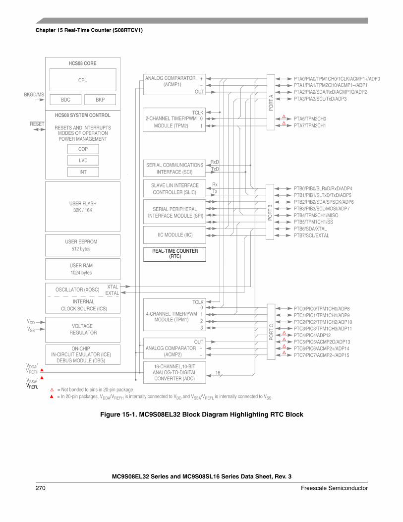
Chapter 15 Real-Time Counter (S08RTCV1)
MC9S08EL32 Series and MC9S08SL16 Series Data Sheet, Rev. 3
270 Freescale Semiconductor
Figure 15-1. MC9S08EL32 Block Diagram Highlighting RTC Block
VSS
IIC MODULE (IIC)
SERIAL PERIPHERAL INTERFACE MODULE (SPI)
USER FLASH
USER RAM
32K / 16K
HCS08 CORE
CPU
BDC
2-CHANNEL TIMER/PWMMODULE (TPM2)
HCS08 SYSTEM CONTROL
RESETS AND INTERRUPTSMODES OF OPERATIONPOWER MANAGEMENT
VOLTAGE REGULATOR
COP
LVD
OSCILLATOR (XOSC)
INTERNALCLOCK SOURCE (ICS)
RESET
VREFH
1024 bytes
INTERFACE (SCI)SERIAL COMMUNICATIONS
XTALEXTAL
4-CHANNEL TIMER/PWMMODULE (TPM1)
REAL-TIME COUNTER
IN-CIRCUIT EMULATOR (ICE)
BKGD/MS PTA3/PIA3/SCL/TxD/ADP3
PTA6/TPM2CH0
PTA2/PIA2/SDA/RxD/ACMP1O/ADP2PTA1/PIA1/TPM2CH0/ACMP1–/ADP1PTA0/PIA0/TPM1CH0/TCLK/ACMP1+/ADP0
PTA7/TPM2CH1
PTB3/PIB3/SCL/MOSI/ADP7PTB4/TPM2CH1/MISO
PTB2/PIB2/SDA/SPSCK/ADP6PTB1/PIB1/SLTxD/TxD/ADP5PTB0/PIB0/SLRxD/RxD/ADP4
PTB7/SCL/EXTAL
PTC3/PIC3/TPM1CH3/ADP11PTC4/PIC4/ADP12PTC5/PIC5/ACMP2O/ADP13
PTC2/PIC2/TPM1CH2/ADP10PTC1/PIC1/TPM1CH1/ADP9
POR
T C
PTC6/PIC6/ACMP2+/ADP14
VDD
BKP
INT
ANALOG COMPARATOR(ACMP2)
USER EEPROM512 bytes
CONTROLLER (SLIC)SLAVE LIN INTERFACE
ANALOG-TO-DIGITALCONVERTER (ADC)
16-CHANNEL,10-BIT16
= In 20-pin packages, VDDA/VREFH is internally connected to VDD and VSSA/VREFL is internally connected to VSS.
VDDA/
VREFL
VSSA/
DEBUG MODULE (DBG)
ON-CHIP
(RTC)
PTC0/PIC0/TPM1CH0/ADP8
PTC7/PIC7/ACMP2–/ADP15
PTB6/SDA/XTAL
POR
T B
POR
T A
PTB5/TPM1CH1/SS
ANALOG COMPARATOR(ACMP1)
= Not bonded to pins in 20-pin package
TCLK
TCLK
+–
OUT
+–
OUT
0123
10
RxDTxD
TxRx

Chapter 15 Real-Time Counter (S08RTCV1)
MC9S08EL32 Series and MC9S08SL16 Series Data Sheet, Rev. 3
Freescale Semiconductor 271
Real-Time Counter (S08RTCV1)
MC9S08EL32 Series and MC9S08SL16 Series Data Sheet, Rev. 3
272 Freescale Semiconductor
15.1.1 Features
Features of the RTC module include:• 8-bit up-counter
— 8-bit modulo match limit— Software controllable periodic interrupt on match
• Three software selectable clock sources for input to prescaler with selectable binary-based and decimal-based divider values— 1-kHz internal low-power oscillator (LPO)— External clock (ERCLK)— 32-kHz internal clock (IRCLK)
15.1.2 Modes of Operation
This section defines the operation in stop, wait and background debug modes.
15.1.2.1 Wait Mode
The RTC continues to run in wait mode if enabled before executing the appropriate instruction. Therefore, the RTC can bring the MCU out of wait mode if the real-time interrupt is enabled. For lowest possible current consumption, the RTC should be stopped by software if not needed as an interrupt source during wait mode.
15.1.2.2 Stop Modes
The RTC continues to run in stop2 or stop3 mode if the RTC is enabled before executing the STOP instruction. Therefore, the RTC can bring the MCU out of stop modes with no external components, if the real-time interrupt is enabled.
The LPO clock can be used in stop2 and stop3 modes. ERCLK and IRCLK clocks are only available in stop3 mode.
Power consumption is lower when all clock sources are disabled, but in that case, the real-time interrupt cannot wake up the MCU from stop modes.
15.1.2.3 Active Background Mode
The RTC suspends all counting during active background mode until the microcontroller returns to normal user operating mode. Counting resumes from the suspended value as long as the RTCMOD register is not written and the RTCPS and RTCLKS bits are not altered.
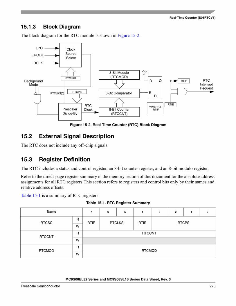
Real-Time Counter (S08RTCV1)
MC9S08EL32 Series and MC9S08SL16 Series Data Sheet, Rev. 3
Freescale Semiconductor 273
15.1.3 Block Diagram
The block diagram for the RTC module is shown in Figure 15-2.
Figure 15-2. Real-Time Counter (RTC) Block Diagram
15.2 External Signal DescriptionThe RTC does not include any off-chip signals.
15.3 Register DefinitionThe RTC includes a status and control register, an 8-bit counter register, and an 8-bit modulo register.
Refer to the direct-page register summary in the memory section of this document for the absolute address assignments for all RTC registers.This section refers to registers and control bits only by their names and relative address offsets.
Table 15-1 is a summary of RTC registers. Table 15-1. RTC Register Summary
Name 7 6 5 4 3 2 1 0
RTCSCR
RTIF RTCLKS RTIE RTCPSW
RTCCNTR RTCCNT
W
RTCMODR
RTCMODW
Clock Source Select
Prescaler Divide-By
8-Bit Counter(RTCCNT)
8-Bit Modulo(RTCMOD)
8-Bit Comparator
RTIF
RTIE
Background
VDD
RTCInterruptRequest
D Q
RE
LPO
RTCClock
Mode
ERCLK
IRCLK
RTCLKS
Write 1 toRTIF
RTCPSRTCLKS[0]
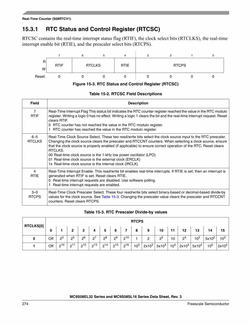
Real-Time Counter (S08RTCV1)
MC9S08EL32 Series and MC9S08SL16 Series Data Sheet, Rev. 3
274 Freescale Semiconductor
15.3.1 RTC Status and Control Register (RTCSC)
RTCSC contains the real-time interrupt status flag (RTIF), the clock select bits (RTCLKS), the real-time interrupt enable bit (RTIE), and the prescaler select bits (RTCPS).
7 6 5 4 3 2 1 0
RRTIF RTCLKS RTIE RTCPS
W
Reset: 0 0 0 0 0 0 0 0
Figure 15-3. RTC Status and Control Register (RTCSC)
Table 15-2. RTCSC Field Descriptions
Field Description
7RTIF
Real-Time Interrupt Flag This status bit indicates the RTC counter register reached the value in the RTC modulo register. Writing a logic 0 has no effect. Writing a logic 1 clears the bit and the real-time interrupt request. Reset clears RTIF.0 RTC counter has not reached the value in the RTC modulo register.1 RTC counter has reached the value in the RTC modulo register.
6–5RTCLKS
Real-Time Clock Source Select. These two read/write bits select the clock source input to the RTC prescaler. Changing the clock source clears the prescaler and RTCCNT counters. When selecting a clock source, ensure that the clock source is properly enabled (if applicable) to ensure correct operation of the RTC. Reset clears RTCLKS.00 Real-time clock source is the 1-kHz low power oscillator (LPO)01 Real-time clock source is the external clock (ERCLK)1x Real-time clock source is the internal clock (IRCLK)
4RTIE
Real-Time Interrupt Enable. This read/write bit enables real-time interrupts. If RTIE is set, then an interrupt is generated when RTIF is set. Reset clears RTIE.0 Real-time interrupt requests are disabled. Use software polling.1 Real-time interrupt requests are enabled.
3–0RTCPS
Real-Time Clock Prescaler Select. These four read/write bits select binary-based or decimal-based divide-by values for the clock source. See Table 15-3. Changing the prescaler value clears the prescaler and RTCCNT counters. Reset clears RTCPS.
Table 15-3. RTC Prescaler Divide-by values
RTCLKS[0]RTCPS
0 1 2 3 4 5 6 7 8 9 10 11 12 13 14 15
0 Off 23 25 26 27 28 29 210 1 2 22 10 24 102 5x10² 103
1 Off 210 211 212 213 214 215 216 103 2x10³ 5x10³ 104 2x10⁴ 5x10⁴ 105 2x10⁵
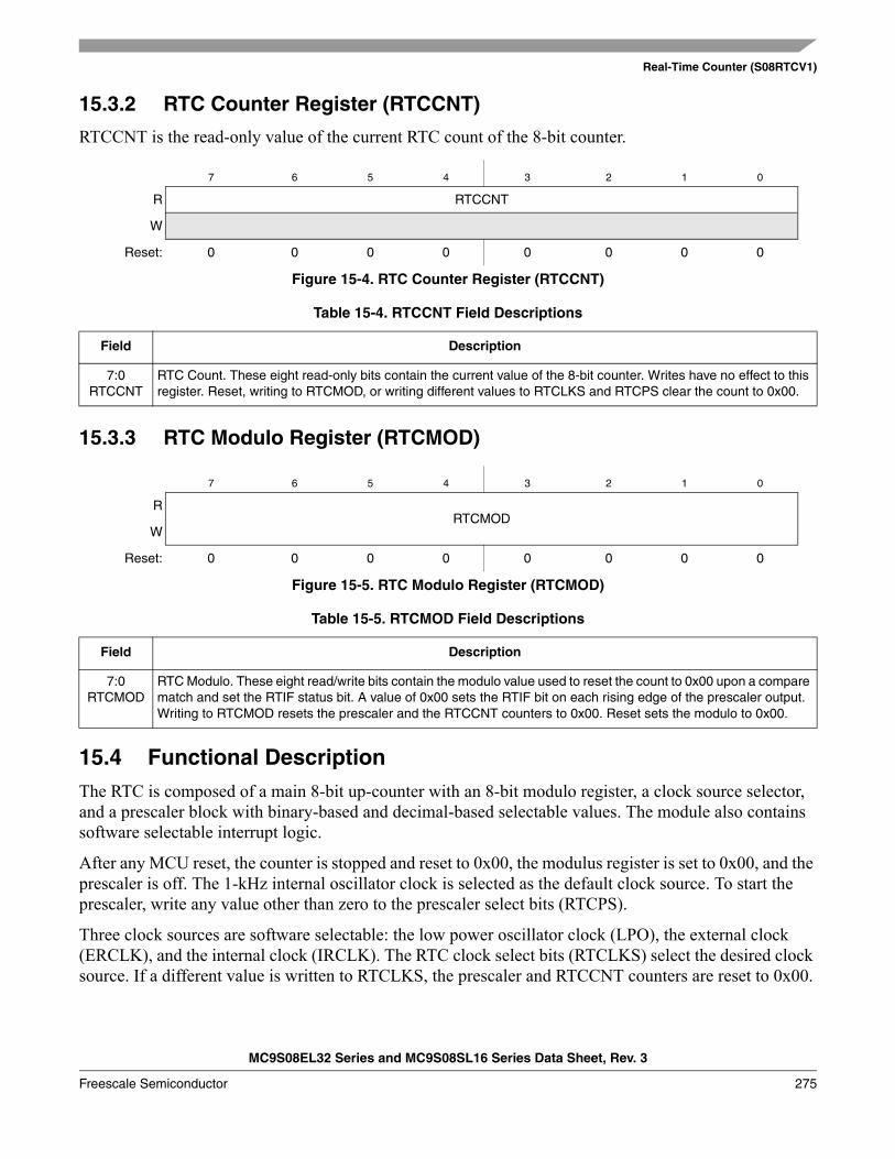
Real-Time Counter (S08RTCV1)
MC9S08EL32 Series and MC9S08SL16 Series Data Sheet, Rev. 3
Freescale Semiconductor 275
15.3.2 RTC Counter Register (RTCCNT)
RTCCNT is the read-only value of the current RTC count of the 8-bit counter.
15.3.3 RTC Modulo Register (RTCMOD)
15.4 Functional DescriptionThe RTC is composed of a main 8-bit up-counter with an 8-bit modulo register, a clock source selector, and a prescaler block with binary-based and decimal-based selectable values. The module also contains software selectable interrupt logic.
After any MCU reset, the counter is stopped and reset to 0x00, the modulus register is set to 0x00, and the prescaler is off. The 1-kHz internal oscillator clock is selected as the default clock source. To start the prescaler, write any value other than zero to the prescaler select bits (RTCPS).
Three clock sources are software selectable: the low power oscillator clock (LPO), the external clock (ERCLK), and the internal clock (IRCLK). The RTC clock select bits (RTCLKS) select the desired clock source. If a different value is written to RTCLKS, the prescaler and RTCCNT counters are reset to 0x00.
7 6 5 4 3 2 1 0
R RTCCNT
W
Reset: 0 0 0 0 0 0 0 0
Figure 15-4. RTC Counter Register (RTCCNT)
Table 15-4. RTCCNT Field Descriptions
Field Description
7:0RTCCNT
RTC Count. These eight read-only bits contain the current value of the 8-bit counter. Writes have no effect to this register. Reset, writing to RTCMOD, or writing different values to RTCLKS and RTCPS clear the count to 0x00.
7 6 5 4 3 2 1 0
RRTCMOD
W
Reset: 0 0 0 0 0 0 0 0
Figure 15-5. RTC Modulo Register (RTCMOD)
Table 15-5. RTCMOD Field Descriptions
Field Description
7:0RTCMOD
RTC Modulo. These eight read/write bits contain the modulo value used to reset the count to 0x00 upon a compare match and set the RTIF status bit. A value of 0x00 sets the RTIF bit on each rising edge of the prescaler output. Writing to RTCMOD resets the prescaler and the RTCCNT counters to 0x00. Reset sets the modulo to 0x00.
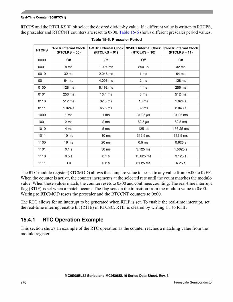
Real-Time Counter (S08RTCV1)
MC9S08EL32 Series and MC9S08SL16 Series Data Sheet, Rev. 3
276 Freescale Semiconductor
RTCPS and the RTCLKS[0] bit select the desired divide-by value. If a different value is written to RTCPS, the prescaler and RTCCNT counters are reset to 0x00. Table 15-6 shows different prescaler period values.
The RTC modulo register (RTCMOD) allows the compare value to be set to any value from 0x00 to 0xFF. When the counter is active, the counter increments at the selected rate until the count matches the modulo value. When these values match, the counter resets to 0x00 and continues counting. The real-time interrupt flag (RTIF) is set when a match occurs. The flag sets on the transition from the modulo value to 0x00. Writing to RTCMOD resets the prescaler and the RTCCNT counters to 0x00.
The RTC allows for an interrupt to be generated when RTIF is set. To enable the real-time interrupt, set the real-time interrupt enable bit (RTIE) in RTCSC. RTIF is cleared by writing a 1 to RTIF.
15.4.1 RTC Operation Example
This section shows an example of the RTC operation as the counter reaches a matching value from the modulo register.
Table 15-6. Prescaler Period
RTCPS1-kHz Internal Clock
(RTCLKS = 00)1-MHz External Clock
(RTCLKS = 01)32-kHz Internal Clock
(RTCLKS = 10)32-kHz Internal Clock
(RTCLKS = 11)
0000 Off Off Off Off
0001 8 ms 1.024 ms 250 μs 32 ms
0010 32 ms 2.048 ms 1 ms 64 ms
0011 64 ms 4.096 ms 2 ms 128 ms
0100 128 ms 8.192 ms 4 ms 256 ms
0101 256 ms 16.4 ms 8 ms 512 ms
0110 512 ms 32.8 ms 16 ms 1.024 s
0111 1.024 s 65.5 ms 32 ms 2.048 s
1000 1 ms 1 ms 31.25 μs 31.25 ms
1001 2 ms 2 ms 62.5 μs 62.5 ms
1010 4 ms 5 ms 125 μs 156.25 ms
1011 10 ms 10 ms 312.5 μs 312.5 ms
1100 16 ms 20 ms 0.5 ms 0.625 s
1101 0.1 s 50 ms 3.125 ms 1.5625 s
1110 0.5 s 0.1 s 15.625 ms 3.125 s
1111 1 s 0.2 s 31.25 ms 6.25 s
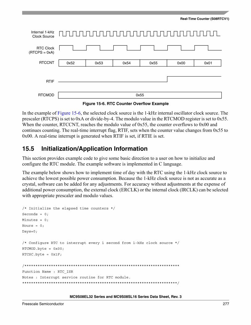
Real-Time Counter (S08RTCV1)
MC9S08EL32 Series and MC9S08SL16 Series Data Sheet, Rev. 3
Freescale Semiconductor 277
Figure 15-6. RTC Counter Overflow Example
In the example of Figure 15-6, the selected clock source is the 1-kHz internal oscillator clock source. The prescaler (RTCPS) is set to 0xA or divide-by-4. The modulo value in the RTCMOD register is set to 0x55. When the counter, RTCCNT, reaches the modulo value of 0x55, the counter overflows to 0x00 and continues counting. The real-time interrupt flag, RTIF, sets when the counter value changes from 0x55 to 0x00. A real-time interrupt is generated when RTIF is set, if RTIE is set.
15.5 Initialization/Application InformationThis section provides example code to give some basic direction to a user on how to initialize and configure the RTC module. The example software is implemented in C language.
The example below shows how to implement time of day with the RTC using the 1-kHz clock source to achieve the lowest possible power consumption. Because the 1-kHz clock source is not as accurate as a crystal, software can be added for any adjustments. For accuracy without adjustments at the expense of additional power consumption, the external clock (ERCLK) or the internal clock (IRCLK) can be selected with appropriate prescaler and modulo values.
/* Initialize the elapsed time counters */
Seconds = 0;
Minutes = 0;
Hours = 0;
Days=0;
/* Configure RTC to interrupt every 1 second from 1-kHz clock source */
RTCMOD.byte = 0x00;
RTCSC.byte = 0x1F;
/**********************************************************************
Function Name : RTC_ISR
Notes : Interrupt service routine for RTC module.
**********************************************************************/
0x55
0x550x540x530x52 0x00 0x01
RTCMOD
RTIF
RTCCNT
RTC Clock(RTCPS = 0xA)
Internal 1-kHzClock Source
Real-Time Counter (S08RTCV1)
MC9S08EL32 Series and MC9S08SL16 Series Data Sheet, Rev. 3
278 Freescale Semiconductor
#pragma TRAP_PROC
void RTC_ISR(void)
{
/* Clear the interrupt flag */
RTCSC.byte = RTCSC.byte | 0x80;
/* RTC interrupts every 1 Second */
Seconds++;
/* 60 seconds in a minute */
if (Seconds > 59){
Minutes++;
Seconds = 0;
}
/* 60 minutes in an hour */
if (Minutes > 59){
Hours++;
Minutes = 0;
}
/* 24 hours in a day */
if (Hours > 23){
Days ++;
Hours = 0;
}
MC9S08EL32 Series and MC9S08SL16 Series Data Sheet, Rev. 3
Freescale Semiconductor 279
Chapter 16 Timer Pulse-Width Modulator (S08TPMV2)
16.1 IntroductionThe TPM uses one input/output (I/O) pin per channel, TPMxCHn where x is the TPM number (for example, 1 or 2) and n is the channel number (for example, 0–4). The TPM shares its I/O pins with general-purpose I/O port pins (refer to the Pins and Connections chapter for more information).
All MC9S08EL32 Series and MC9S08SL16 Series MCUs have two TPM modules. In all packages, TPM2 is 2-channel. The number of channels available in TPM1 depends on the device, as shown in Table 16-1:
t
Table 16-1. MC9S08EL32 Series and MC9S08SL16 Series Features by MCU and Package
Feature 9S08EL32 9S08EL16 9S08SL16 9S08SL8
Pin quantity 28 20 28 20 28 20 28 20
Package type TSSOP TSSOP TSSOP TSSOP TSSOP TSSOP TSSOP TSSOP
TPM1 channels 4 2
TPM2 channels 2 2
Chapter 16 Timer Pulse-Width Modulator (S08TPMV2)
MC9S08EL32 Series and MC9S08SL16 Series Data Sheet, Rev. 3
280 Freescale Semiconductor
Figure 16-1. MC9S08EL32 Block Diagram Highlighting TPM Block and Pins
VSS
IIC MODULE (IIC)
SERIAL PERIPHERAL INTERFACE MODULE (SPI)
USER FLASH
USER RAM
32K / 16K
HCS08 CORE
CPU
BDC
2-CHANNEL TIMER/PWMMODULE (TPM2)
HCS08 SYSTEM CONTROL
RESETS AND INTERRUPTSMODES OF OPERATIONPOWER MANAGEMENT
VOLTAGE REGULATOR
COP
LVD
OSCILLATOR (XOSC)
INTERNALCLOCK SOURCE (ICS)
RESET
VREFH
1024 bytes
INTERFACE (SCI)SERIAL COMMUNICATIONS
XTALEXTAL
4-CHANNEL TIMER/PWMMODULE (TPM1)
REAL-TIME COUNTER
IN-CIRCUIT EMULATOR (ICE)
BKGD/MS PTA3/PIA3/SCL/TxD/ADP3
PTA6/TPM2CH0
PTA2/PIA2/SDA/RxD/ACMP1O/ADP2PTA1/PIA1/TPM2CH0/ACMP1–/ADP1PTA0/PIA0/TPM1CH0/TCLK/ACMP1+/ADP0
PTA7/TPM2CH1
PTB3/PIB3/SCL/MOSI/ADP7PTB4/TPM2CH1/MISO
PTB2/PIB2/SDA/SPSCK/ADP6PTB1/PIB1/SLTxD/TxD/ADP5PTB0/PIB0/SLRxD/RxD/ADP4
PTB7/SCL/EXTAL
PTC3/PIC3/TPM1CH3/ADP11PTC4/PIC4/ADP12PTC5/PIC5/ACMP2O/ADP13
PTC2/PIC2/TPM1CH2/ADP10PTC1/PIC1/TPM1CH1/ADP9
POR
T C
PTC6/PIC6/ACMP2+/ADP14
VDD
BKP
INT
ANALOG COMPARATOR(ACMP2)
USER EEPROM512 bytes
CONTROLLER (SLIC)SLAVE LIN INTERFACE
ANALOG-TO-DIGITALCONVERTER (ADC)
16-CHANNEL,10-BIT16
= In 20-pin packages, VDDA/VREFH is internally connected to VDD and VSSA/VREFL is internally connected to VSS.
VDDA/
VREFL
VSSA/
DEBUG MODULE (DBG)
ON-CHIP
(RTC)
PTC0/PIC0/TPM1CH0/ADP8
PTC7/PIC7/ACMP2–/ADP15
PTB6/SDA/XTAL
POR
T B
POR
T A
PTB5/TPM1CH1/SS
ANALOG COMPARATOR(ACMP1)
= Not bonded to pins in 20-pin package
TCLK
TCLK
+–
OUT
+–
OUT
0123
10
RxDTxD
TxRx
Timer/PWM Module (S08TPMV3)
MC9S08EL32 Series and MC9S08SL16 Series Data Sheet, Rev. 3
Freescale Semiconductor 281
16.1.1 Features
The TPM includes these distinctive features:• One to eight channels:
— Each channel may be input capture, output compare, or edge-aligned PWM— Rising-Edge, falling-edge, or any-edge input capture trigger— Set, clear, or toggle output compare action— Selectable polarity on PWM outputs
• Module may be configured for buffered, center-aligned pulse-width-modulation (CPWM) on all channels
• Timer clock source selectable as prescaled bus clock, fixed system clock, or an external clock pin— Prescale taps for divide-by 1, 2, 4, 8, 16, 32, 64, or 128— Fixed system clock source are synchronized to the bus clock by an on-chip synchronization
circuit— External clock pin may be shared with any timer channel pin or a separated input pin
• 16-bit free-running or modulo up/down count operation• Timer system enable• One interrupt per channel plus terminal count interrupt
16.1.2 Modes of Operation
In general, TPM channels may be independently configured to operate in input capture, output compare, or edge-aligned PWM modes. A control bit allows the whole TPM (all channels) to switch to center-aligned PWM mode. When center-aligned PWM mode is selected, input capture, output compare, and edge-aligned PWM functions are not available on any channels of this TPM module.
When the microcontroller is in active BDM background or BDM foreground mode, the TPM temporarily suspends all counting until the microcontroller returns to normal user operating mode. During stop mode, all system clocks, including the main oscillator, are stopped; therefore, the TPM is effectively disabled until clocks resume. During wait mode, the TPM continues to operate normally. Provided the TPM does not need to produce a real time reference or provide the interrupt source(s) needed to wake the MCU from wait mode, the user can save power by disabling TPM functions before entering wait mode.
• Input capture modeWhen a selected edge event occurs on the associated MCU pin, the current value of the 16-bit timer counter is captured into the channel value register and an interrupt flag bit is set. Rising edges, falling edges, any edge, or no edge (disable channel) may be selected as the active edge which triggers the input capture.
• Output compare modeWhen the value in the timer counter register matches the channel value register, an interrupt flag bit is set, and a selected output action is forced on the associated MCU pin. The output compare action may be selected to force the pin to zero, force the pin to one, toggle the pin, or ignore the pin (used for software timing functions).
Timer/PWM Module (S08TPMV3)
MC9S08EL32 Series and MC9S08SL16 Series Data Sheet, Rev. 3
282 Freescale Semiconductor
• Edge-aligned PWM modeThe value of a 16-bit modulo register plus 1 sets the period of the PWM output signal. The channel value register sets the duty cycle of the PWM output signal. The user may also choose the polarity of the PWM output signal. Interrupts are available at the end of the period and at the duty-cycle transition point. This type of PWM signal is called edge-aligned because the leading edges of all PWM signals are aligned with the beginning of the period, which is the same for all channels within a TPM.
• Center-aligned PWM modeTwice the value of a 16-bit modulo register sets the period of the PWM output, and the channel-value register sets the half-duty-cycle duration. The timer counter counts up until it reaches the modulo value and then counts down until it reaches zero. As the count matches the channel value register while counting down, the PWM output becomes active. When the count matches the channel value register while counting up, the PWM output becomes inactive. This type of PWM signal is called center-aligned because the centers of the active duty cycle periods for all channels are aligned with a count value of zero. This type of PWM is required for types of motors used in small appliances.
This is a high-level description only. Detailed descriptions of operating modes are in later sections.
16.1.3 Block Diagram
The TPM uses one input/output (I/O) pin per channel, TPMxCHn (timer channel n) where n is the channel number (1-8). The TPM shares its I/O pins with general purpose I/O port pins (refer to I/O pin descriptions in full-chip specification for the specific chip implementation).
Figure 16-2 shows the TPM structure. The central component of the TPM is the 16-bit counter that can operate as a free-running counter or a modulo up/down counter. The TPM counter (when operating in normal up-counting mode) provides the timing reference for the input capture, output compare, and edge-aligned PWM functions. The timer counter modulo registers, TPMxMODH:TPMxMODL, control the modulo value of the counter (the values 0x0000 or 0xFFFF effectively make the counter free running). Software can read the counter value at any time without affecting the counting sequence. Any write to either half of the TPMxCNT counter resets the counter, regardless of the data value written.
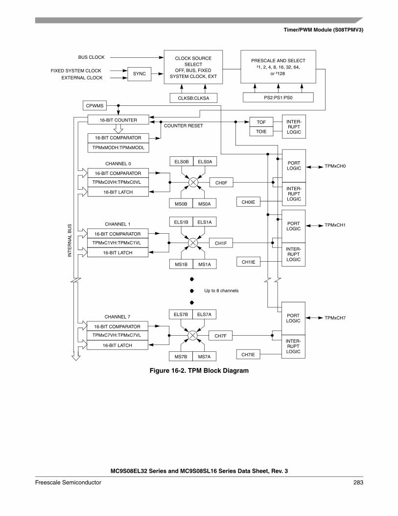
Timer/PWM Module (S08TPMV3)
MC9S08EL32 Series and MC9S08SL16 Series Data Sheet, Rev. 3
Freescale Semiconductor 283
Figure 16-2. TPM Block Diagram
PRESCALE AND SELECT
16-BIT COMPARATOR
PS2:PS1:PS0
TOF
TOIE
INTER-16-BIT COUNTER
RUPTLOGIC
16-BIT COMPARATOR
16-BIT LATCH
ELS0B ELS0A PORTCHANNEL 0
CH0IE
CH0F
LOGIC
INTER-RUPTLOGIC
CPWMS
MS0B MS0A
COUNTER RESET
CLKSB:CLKSA
³1, 2, 4, 8, 16, 32, 64,
BUS CLOCK
FIXED SYSTEM CLOCK
EXTERNAL CLOCKSYNC
16-BIT COMPARATOR
16-BIT LATCH
CHANNEL 1 ELS1B ELS1A
CH1IE
CH1F
INT
ER
NA
L B
US PORT
LOGIC
INTER-RUPTLOGIC
MS1B MS1A
16-BIT COMPARATOR
16-BIT LATCH
CHANNEL 7 ELS7B ELS7A
CH7IE
CH7F
PORTLOGIC
INTER-RUPTLOGIC
MS7B MS7A
Up to 8 channels
CLOCK SOURCESELECT
OFF, BUS, FIXEDSYSTEM CLOCK, EXT
or ³128
TPMxMODH:TPMxMODL
TPMxC0VH:TPMxC0VL
TPMxC1VH:TPMxC1VL
TPMxCH0
TPMxCH1
TPMxC7VH:TPMxC7VL
TPMxCH7
Timer/PWM Module (S08TPMV3)
MC9S08EL32 Series and MC9S08SL16 Series Data Sheet, Rev. 3
284 Freescale Semiconductor
The TPM channels are programmable independently as input capture, output compare, or edge-aligned PWM channels. Alternately, the TPM can be configured to produce CPWM outputs on all channels. When the TPM is configured for CPWMs, the counter operates as an up/down counter; input capture, output compare, and EPWM functions are not practical.
If a channel is configured as input capture, an internal pullup device may be enabled for that channel. The details of how a module interacts with pin controls depends upon the chip implementation because the I/O pins and associated general purpose I/O controls are not part of the module. Refer to the discussion of the I/O port logic in a full-chip specification.
Because center-aligned PWMs are usually used to drive 3-phase AC-induction motors and brushless DC motors, they are typically used in sets of three or six channels.
16.2 Signal DescriptionTable 16-2 shows the user-accessible signals for the TPM. The number of channels may be varied from one to eight. When an external clock is included, it can be shared with the same pin as any TPM channel; however, it could be connected to a separate input pin. Refer to the I/O pin descriptions in full-chip specification for the specific chip implementation.
Refer to documentation for the full-chip for details about reset states, port connections, and whether there is any pullup device on these pins.
TPM channel pins can be associated with general purpose I/O pins and have passive pullup devices which can be enabled with a control bit when the TPM or general purpose I/O controls have configured the associated pin as an input. When no TPM function is enabled to use a corresponding pin, the pin reverts to being controlled by general purpose I/O controls, including the port-data and data-direction registers. Immediately after reset, no TPM functions are enabled, so all associated pins revert to general purpose I/O control.
16.2.1 Detailed Signal Descriptions
This section describes each user-accessible pin signal in detail. Although Table 16-2 grouped all channel pins together, any TPM pin can be shared with the external clock source signal. Since I/O pin logic is not part of the TPM, refer to full-chip documentation for a specific derivative for more details about the interaction of TPM pin functions and general purpose I/O controls including port data, data direction, and pullup controls.
Table 16-2. Signal Properties
Name Function
EXTCLK1
1 When preset, this signal can share any channel pin; however depending upon full-chip implementation, this signal could be connected to a separate external pin.
External clock source which may be selected to drive the TPM counter.
TPMxCHn2
2 n=channel number (1 to 8)
I/O pin associated with TPM channel n
Timer/PWM Module (S08TPMV3)
MC9S08EL32 Series and MC9S08SL16 Series Data Sheet, Rev. 3
Freescale Semiconductor 285
16.2.1.1 EXTCLK — External Clock Source
Control bits in the timer status and control register allow the user to select nothing (timer disable), the bus-rate clock (the normal default source), a crystal-related clock, or an external clock as the clock which drives the TPM prescaler and subsequently the 16-bit TPM counter. The external clock source is synchronized in the TPM. The bus clock clocks the synchronizer; the frequency of the external source must be no more than one-fourth the frequency of the bus-rate clock, to meet Nyquist criteria and allowing for jitter.
The external clock signal shares the same pin as a channel I/O pin, so the channel pin will not be usable for channel I/O function when selected as the external clock source. It is the user’s responsibility to avoid such settings. If this pin is used as an external clock source (CLKSB:CLKSA = 1:1), the channel can still be used in output compare mode as a software timer (ELSnB:ELSnA = 0:0).
16.2.1.2 TPMxCHn — TPM Channel n I/O Pin(s)
Each TPM channel is associated with an I/O pin on the MCU. The function of this pin depends on the channel configuration. The TPM pins share with general purpose I/O pins, where each pin has a port data register bit, and a data direction control bit, and the port has optional passive pullups which may be enabled whenever a port pin is acting as an input.
The TPM channel does not control the I/O pin when (ELSnB:ELSnA = 0:0) or when (CLKSB:CLKSA = 0:0) so it normally reverts to general purpose I/O control. When CPWMS = 1 (and ELSnB:ELSnA not = 0:0), all channels within the TPM are configured for center-aligned PWM and the TPMxCHn pins are all controlled by the TPM system. When CPWMS=0, the MSnB:MSnA control bits determine whether the channel is configured for input capture, output compare, or edge-aligned PWM.
When a channel is configured for input capture (CPWMS=0, MSnB:MSnA = 0:0 and ELSnB:ELSnA not = 0:0), the TPMxCHn pin is forced to act as an edge-sensitive input to the TPM. ELSnB:ELSnA control bits determine what polarity edge or edges will trigger input-capture events. A synchronizer based on the bus clock is used to synchronize input edges to the bus clock. This implies the minimum pulse width—that can be reliably detected—on an input capture pin is four bus clock periods (with ideal clock pulses as near as two bus clocks can be detected). TPM uses this pin as an input capture input to override the port data and data direction controls for the same pin.
When a channel is configured for output compare (CPWMS=0, MSnB:MSnA = 0:1 and ELSnB:ELSnA not = 0:0), the associated data direction control is overridden, the TPMxCHn pin is considered an output controlled by the TPM, and the ELSnB:ELSnA control bits determine how the pin is controlled. The remaining three combinations of ELSnB:ELSnA determine whether the TPMxCHn pin is toggled, cleared, or set each time the 16-bit channel value register matches the timer counter.
When the output compare toggle mode is initially selected, the previous value on the pin is driven out until the next output compare event—then the pin is toggled.
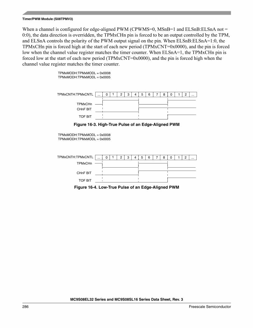
Timer/PWM Module (S08TPMV3)
MC9S08EL32 Series and MC9S08SL16 Series Data Sheet, Rev. 3
286 Freescale Semiconductor
When a channel is configured for edge-aligned PWM (CPWMS=0, MSnB=1 and ELSnB:ELSnA not = 0:0), the data direction is overridden, the TPMxCHn pin is forced to be an output controlled by the TPM, and ELSnA controls the polarity of the PWM output signal on the pin. When ELSnB:ELSnA=1:0, the TPMxCHn pin is forced high at the start of each new period (TPMxCNT=0x0000), and the pin is forced low when the channel value register matches the timer counter. When ELSnA=1, the TPMxCHn pin is forced low at the start of each new period (TPMxCNT=0x0000), and the pin is forced high when the channel value register matches the timer counter.
Figure 16-3. High-True Pulse of an Edge-Aligned PWM
Figure 16-4. Low-True Pulse of an Edge-Aligned PWM
CHnF BIT
TOF BIT
0... 1 2 3 4 5 6 7 8 0 1 2 ...
TPMxMODH:TPMxMODL = 0x0008TPMxMODH:TPMxMODL = 0x0005
TPMxCNTH:TPMxCNTL
TPMxCHn
CHnF BIT
TOF BIT
0... 1 2 3 4 5 6 7 8 0 1 2 ...
TPMxMODH:TPMxMODL = 0x0008TPMxMODH:TPMxMODL = 0x0005
TPMxCNTH:TPMxCNTL
TPMxCHn
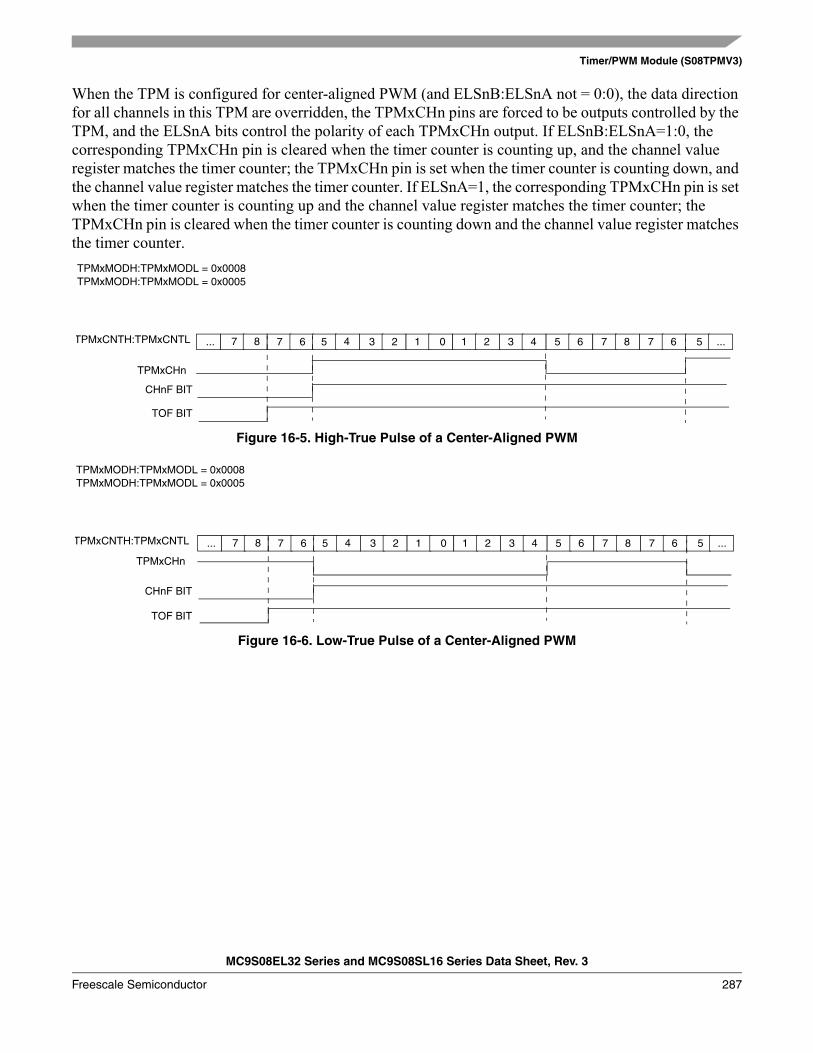
Timer/PWM Module (S08TPMV3)
MC9S08EL32 Series and MC9S08SL16 Series Data Sheet, Rev. 3
Freescale Semiconductor 287
When the TPM is configured for center-aligned PWM (and ELSnB:ELSnA not = 0:0), the data direction for all channels in this TPM are overridden, the TPMxCHn pins are forced to be outputs controlled by the TPM, and the ELSnA bits control the polarity of each TPMxCHn output. If ELSnB:ELSnA=1:0, the corresponding TPMxCHn pin is cleared when the timer counter is counting up, and the channel value register matches the timer counter; the TPMxCHn pin is set when the timer counter is counting down, and the channel value register matches the timer counter. If ELSnA=1, the corresponding TPMxCHn pin is set when the timer counter is counting up and the channel value register matches the timer counter; the TPMxCHn pin is cleared when the timer counter is counting down and the channel value register matches the timer counter.
Figure 16-5. High-True Pulse of a Center-Aligned PWM
Figure 16-6. Low-True Pulse of a Center-Aligned PWM
CHnF BIT
TOF BIT
... 7 8 7 6 5 4 3 2 1 0 1 2 3 4 5 6 7 8 7 6 5 ...
TPMxMODH:TPMxMODL = 0x0008TPMxMODH:TPMxMODL = 0x0005
TPMxCNTH:TPMxCNTL
TPMxCHn
CHnF BIT
TOF BIT
... 7 8 7 6 5 4 3 2 1 0 1 2 3 4 5 6 7 8 7 6 5 ...
TPMxMODH:TPMxMODL = 0x0008TPMxMODH:TPMxMODL = 0x0005
TPMxCNTH:TPMxCNTL
TPMxCHn
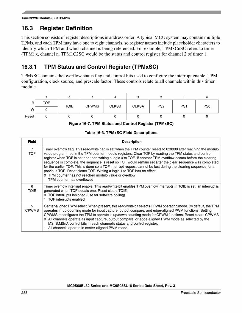
Timer/PWM Module (S08TPMV3)
MC9S08EL32 Series and MC9S08SL16 Series Data Sheet, Rev. 3
288 Freescale Semiconductor
16.3 Register DefinitionThis section consists of register descriptions in address order. A typical MCU system may contain multiple TPMs, and each TPM may have one to eight channels, so register names include placeholder characters to identify which TPM and which channel is being referenced. For example, TPMxCnSC refers to timer (TPM) x, channel n. TPM1C2SC would be the status and control register for channel 2 of timer 1.
16.3.1 TPM Status and Control Register (TPMxSC)
TPMxSC contains the overflow status flag and control bits used to configure the interrupt enable, TPM configuration, clock source, and prescale factor. These controls relate to all channels within this timer module.
7 6 5 4 3 2 1 0
R TOFTOIE CPWMS CLKSB CLKSA PS2 PS1 PS0
W 0
Reset 0 0 0 0 0 0 0 0
Figure 16-7. TPM Status and Control Register (TPMxSC)
Table 16-3. TPMxSC Field Descriptions
Field Description
7TOF
Timer overflow flag. This read/write flag is set when the TPM counter resets to 0x0000 after reaching the modulo value programmed in the TPM counter modulo registers. Clear TOF by reading the TPM status and control register when TOF is set and then writing a logic 0 to TOF. If another TPM overflow occurs before the clearing sequence is complete, the sequence is reset so TOF would remain set after the clear sequence was completed for the earlier TOF. This is done so a TOF interrupt request cannot be lost during the clearing sequence for a previous TOF. Reset clears TOF. Writing a logic 1 to TOF has no effect.0 TPM counter has not reached modulo value or overflow1 TPM counter has overflowed
6TOIE
Timer overflow interrupt enable. This read/write bit enables TPM overflow interrupts. If TOIE is set, an interrupt is generated when TOF equals one. Reset clears TOIE.0 TOF interrupts inhibited (use for software polling)1 TOF interrupts enabled
5CPWMS
Center-aligned PWM select. When present, this read/write bit selects CPWM operating mode. By default, the TPM operates in up-counting mode for input capture, output compare, and edge-aligned PWM functions. Setting CPWMS reconfigures the TPM to operate in up/down counting mode for CPWM functions. Reset clears CPWMS.0 All channels operate as input capture, output compare, or edge-aligned PWM mode as selected by the
MSnB:MSnA control bits in each channel’s status and control register.1 All channels operate in center-aligned PWM mode.
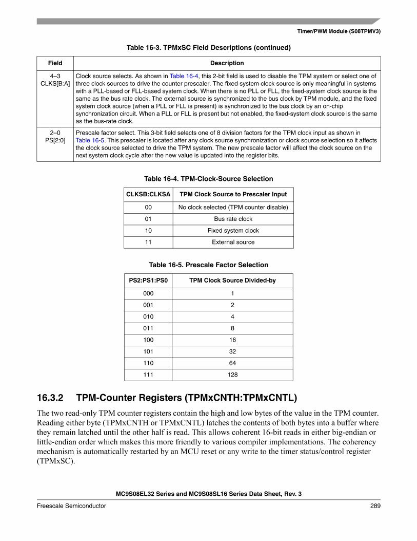
Timer/PWM Module (S08TPMV3)
MC9S08EL32 Series and MC9S08SL16 Series Data Sheet, Rev. 3
Freescale Semiconductor 289
16.3.2 TPM-Counter Registers (TPMxCNTH:TPMxCNTL)
The two read-only TPM counter registers contain the high and low bytes of the value in the TPM counter. Reading either byte (TPMxCNTH or TPMxCNTL) latches the contents of both bytes into a buffer where they remain latched until the other half is read. This allows coherent 16-bit reads in either big-endian or little-endian order which makes this more friendly to various compiler implementations. The coherency mechanism is automatically restarted by an MCU reset or any write to the timer status/control register (TPMxSC).
4–3CLKS[B:A]
Clock source selects. As shown in Table 16-4, this 2-bit field is used to disable the TPM system or select one of three clock sources to drive the counter prescaler. The fixed system clock source is only meaningful in systems with a PLL-based or FLL-based system clock. When there is no PLL or FLL, the fixed-system clock source is the same as the bus rate clock. The external source is synchronized to the bus clock by TPM module, and the fixed system clock source (when a PLL or FLL is present) is synchronized to the bus clock by an on-chip synchronization circuit. When a PLL or FLL is present but not enabled, the fixed-system clock source is the same as the bus-rate clock.
2–0PS[2:0]
Prescale factor select. This 3-bit field selects one of 8 division factors for the TPM clock input as shown in Table 16-5. This prescaler is located after any clock source synchronization or clock source selection so it affects the clock source selected to drive the TPM system. The new prescale factor will affect the clock source on the next system clock cycle after the new value is updated into the register bits.
Table 16-4. TPM-Clock-Source Selection
CLKSB:CLKSA TPM Clock Source to Prescaler Input
00 No clock selected (TPM counter disable)
01 Bus rate clock
10 Fixed system clock
11 External source
Table 16-5. Prescale Factor Selection
PS2:PS1:PS0 TPM Clock Source Divided-by
000 1
001 2
010 4
011 8
100 16
101 32
110 64
111 128
Table 16-3. TPMxSC Field Descriptions (continued)
Field Description
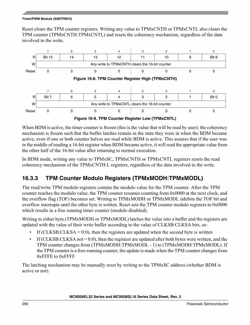
Timer/PWM Module (S08TPMV3)
MC9S08EL32 Series and MC9S08SL16 Series Data Sheet, Rev. 3
290 Freescale Semiconductor
Reset clears the TPM counter registers. Writing any value to TPMxCNTH or TPMxCNTL also clears the TPM counter (TPMxCNTH:TPMxCNTL) and resets the coherency mechanism, regardless of the data involved in the write.
When BDM is active, the timer counter is frozen (this is the value that will be read by user); the coherency mechanism is frozen such that the buffer latches remain in the state they were in when the BDM became active, even if one or both counter halves are read while BDM is active. This assures that if the user was in the middle of reading a 16-bit register when BDM became active, it will read the appropriate value from the other half of the 16-bit value after returning to normal execution.
In BDM mode, writing any value to TPMxSC, TPMxCNTH or TPMxCNTL registers resets the read coherency mechanism of the TPMxCNTH:L registers, regardless of the data involved in the write.
16.3.3 TPM Counter Modulo Registers (TPMxMODH:TPMxMODL)
The read/write TPM modulo registers contain the modulo value for the TPM counter. After the TPM counter reaches the modulo value, the TPM counter resumes counting from 0x0000 at the next clock, and the overflow flag (TOF) becomes set. Writing to TPMxMODH or TPMxMODL inhibits the TOF bit and overflow interrupts until the other byte is written. Reset sets the TPM counter modulo registers to 0x0000 which results in a free running timer counter (modulo disabled).
Writing to either byte (TPMxMODH or TPMxMODL) latches the value into a buffer and the registers are updated with the value of their write buffer according to the value of CLKSB:CLKSA bits, so:
• If (CLKSB:CLKSA = 0:0), then the registers are updated when the second byte is written• If (CLKSB:CLKSA not = 0:0), then the registers are updated after both bytes were written, and the
TPM counter changes from (TPMxMODH:TPMxMODL - 1) to (TPMxMODH:TPMxMODL). If the TPM counter is a free-running counter, the update is made when the TPM counter changes from 0xFFFE to 0xFFFF
The latching mechanism may be manually reset by writing to the TPMxSC address (whether BDM is active or not).
7 6 5 4 3 2 1 0
R Bit 15 14 13 12 11 10 9 Bit 8
W Any write to TPMxCNTH clears the 16-bit counter
Reset 0 0 0 0 0 0 0 0
Figure 16-8. TPM Counter Register High (TPMxCNTH)
7 6 5 4 3 2 1 0
R Bit 7 6 5 4 3 2 1 Bit 0
W Any write to TPMxCNTL clears the 16-bit counter
Reset 0 0 0 0 0 0 0 0
Figure 16-9. TPM Counter Register Low (TPMxCNTL)
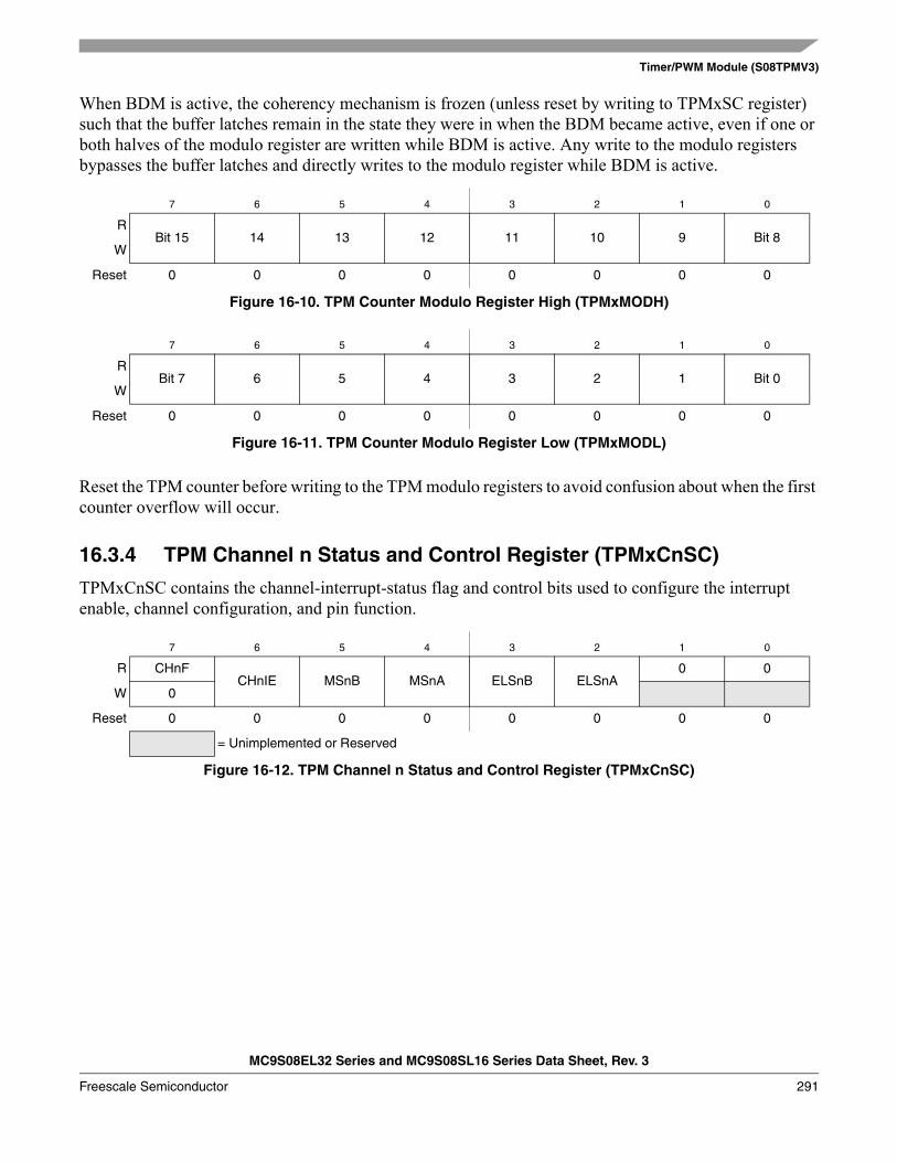
Timer/PWM Module (S08TPMV3)
MC9S08EL32 Series and MC9S08SL16 Series Data Sheet, Rev. 3
Freescale Semiconductor 291
When BDM is active, the coherency mechanism is frozen (unless reset by writing to TPMxSC register) such that the buffer latches remain in the state they were in when the BDM became active, even if one or both halves of the modulo register are written while BDM is active. Any write to the modulo registers bypasses the buffer latches and directly writes to the modulo register while BDM is active.
Reset the TPM counter before writing to the TPM modulo registers to avoid confusion about when the first counter overflow will occur.
16.3.4 TPM Channel n Status and Control Register (TPMxCnSC)
TPMxCnSC contains the channel-interrupt-status flag and control bits used to configure the interrupt enable, channel configuration, and pin function.
7 6 5 4 3 2 1 0
RBit 15 14 13 12 11 10 9 Bit 8
W
Reset 0 0 0 0 0 0 0 0
Figure 16-10. TPM Counter Modulo Register High (TPMxMODH)
7 6 5 4 3 2 1 0
RBit 7 6 5 4 3 2 1 Bit 0
W
Reset 0 0 0 0 0 0 0 0
Figure 16-11. TPM Counter Modulo Register Low (TPMxMODL)
7 6 5 4 3 2 1 0
R CHnFCHnIE MSnB MSnA ELSnB ELSnA
0 0
W 0
Reset 0 0 0 0 0 0 0 0
= Unimplemented or Reserved
Figure 16-12. TPM Channel n Status and Control Register (TPMxCnSC)
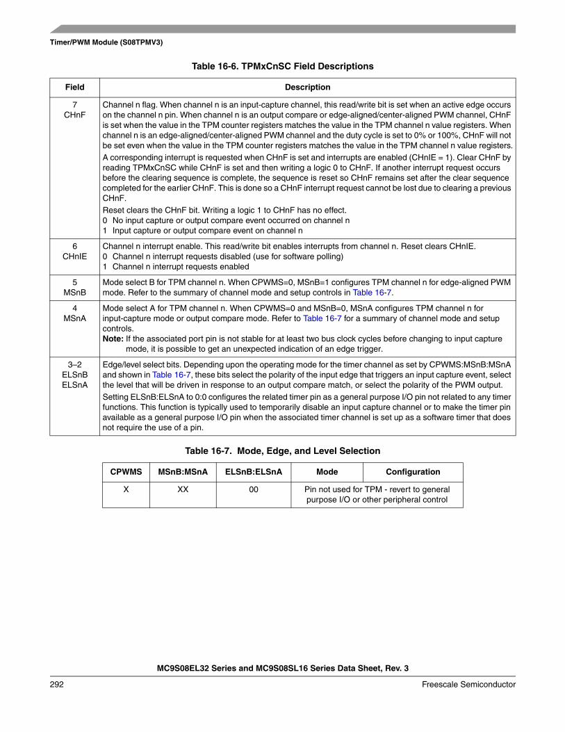
Timer/PWM Module (S08TPMV3)
MC9S08EL32 Series and MC9S08SL16 Series Data Sheet, Rev. 3
292 Freescale Semiconductor
Table 16-6. TPMxCnSC Field Descriptions
Field Description
7CHnF
Channel n flag. When channel n is an input-capture channel, this read/write bit is set when an active edge occurs on the channel n pin. When channel n is an output compare or edge-aligned/center-aligned PWM channel, CHnF is set when the value in the TPM counter registers matches the value in the TPM channel n value registers. When channel n is an edge-aligned/center-aligned PWM channel and the duty cycle is set to 0% or 100%, CHnF will not be set even when the value in the TPM counter registers matches the value in the TPM channel n value registers.A corresponding interrupt is requested when CHnF is set and interrupts are enabled (CHnIE = 1). Clear CHnF by reading TPMxCnSC while CHnF is set and then writing a logic 0 to CHnF. If another interrupt request occurs before the clearing sequence is complete, the sequence is reset so CHnF remains set after the clear sequence completed for the earlier CHnF. This is done so a CHnF interrupt request cannot be lost due to clearing a previous CHnF.Reset clears the CHnF bit. Writing a logic 1 to CHnF has no effect.0 No input capture or output compare event occurred on channel n1 Input capture or output compare event on channel n
6CHnIE
Channel n interrupt enable. This read/write bit enables interrupts from channel n. Reset clears CHnIE.0 Channel n interrupt requests disabled (use for software polling)1 Channel n interrupt requests enabled
5MSnB
Mode select B for TPM channel n. When CPWMS=0, MSnB=1 configures TPM channel n for edge-aligned PWM mode. Refer to the summary of channel mode and setup controls in Table 16-7.
4MSnA
Mode select A for TPM channel n. When CPWMS=0 and MSnB=0, MSnA configures TPM channel n for input-capture mode or output compare mode. Refer to Table 16-7 for a summary of channel mode and setup controls.Note: If the associated port pin is not stable for at least two bus clock cycles before changing to input capture
mode, it is possible to get an unexpected indication of an edge trigger.
3–2ELSnBELSnA
Edge/level select bits. Depending upon the operating mode for the timer channel as set by CPWMS:MSnB:MSnA and shown in Table 16-7, these bits select the polarity of the input edge that triggers an input capture event, select the level that will be driven in response to an output compare match, or select the polarity of the PWM output.
Setting ELSnB:ELSnA to 0:0 configures the related timer pin as a general purpose I/O pin not related to any timer functions. This function is typically used to temporarily disable an input capture channel or to make the timer pin available as a general purpose I/O pin when the associated timer channel is set up as a software timer that does not require the use of a pin.
Table 16-7. Mode, Edge, and Level Selection
CPWMS MSnB:MSnA ELSnB:ELSnA Mode Configuration
X XX 00 Pin not used for TPM - revert to general purpose I/O or other peripheral control
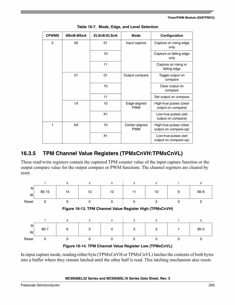
Timer/PWM Module (S08TPMV3)
MC9S08EL32 Series and MC9S08SL16 Series Data Sheet, Rev. 3
Freescale Semiconductor 293
16.3.5 TPM Channel Value Registers (TPMxCnVH:TPMxCnVL)
These read/write registers contain the captured TPM counter value of the input capture function or the output compare value for the output compare or PWM functions. The channel registers are cleared by reset.
In input capture mode, reading either byte (TPMxCnVH or TPMxCnVL) latches the contents of both bytes into a buffer where they remain latched until the other half is read. This latching mechanism also resets
0 00 01 Input capture Capture on rising edge only
10 Capture on falling edge only
11 Capture on rising or falling edge
01 01 Output compare Toggle output on compare
10 Clear output on compare
11 Set output on compare
1X 10 Edge-aligned PWM
High-true pulses (clear output on compare)
X1 Low-true pulses (set output on compare)
1 XX 10 Center-aligned PWM
High-true pulses (clear output on compare-up)
X1 Low-true pulses (set output on compare-up)
7 6 5 4 3 2 1 0
RBit 15 14 13 12 11 10 9 Bit 8
W
Reset 0 0 0 0 0 0 0 0
Figure 16-13. TPM Channel Value Register High (TPMxCnVH)
7 6 5 4 3 2 1 0
RBit 7 6 5 4 3 2 1 Bit 0
W
Reset 0 0 0 0 0 0 0 0
Figure 16-14. TPM Channel Value Register Low (TPMxCnVL)
Table 16-7. Mode, Edge, and Level Selection
CPWMS MSnB:MSnA ELSnB:ELSnA Mode Configuration
Timer/PWM Module (S08TPMV3)
MC9S08EL32 Series and MC9S08SL16 Series Data Sheet, Rev. 3
294 Freescale Semiconductor
(becomes unlatched) when the TPMxCnSC register is written (whether BDM mode is active or not). Any write to the channel registers will be ignored during the input capture mode.
When BDM is active, the coherency mechanism is frozen (unless reset by writing to TPMxCnSC register) such that the buffer latches remain in the state they were in when the BDM became active, even if one or both halves of the channel register are read while BDM is active. This assures that if the user was in the middle of reading a 16-bit register when BDM became active, it will read the appropriate value from the other half of the 16-bit value after returning to normal execution. The value read from the TPMxCnVH and TPMxCnVL registers in BDM mode is the value of these registers and not the value of their read buffer.
In output compare or PWM modes, writing to either byte (TPMxCnVH or TPMxCnVL) latches the value into a buffer. After both bytes are written, they are transferred as a coherent 16-bit value into the timer-channel registers according to the value of CLKSB:CLKSA bits and the selected mode, so:
• If (CLKSB:CLKSA = 0:0), then the registers are updated when the second byte is written.• If (CLKSB:CLKSA not = 0:0 and in output compare mode) then the registers are updated after the
second byte is written and on the next change of the TPM counter (end of the prescaler counting).• If (CLKSB:CLKSA not = 0:0 and in EPWM or CPWM modes), then the registers are updated after
the both bytes were written, and the TPM counter changes from (TPMxMODH:TPMxMODL - 1) to (TPMxMODH:TPMxMODL). If the TPM counter is a free-running counter then the update is made when the TPM counter changes from 0xFFFE to 0xFFFF.
The latching mechanism may be manually reset by writing to the TPMxCnSC register (whether BDM mode is active or not). This latching mechanism allows coherent 16-bit writes in either big-endian or little-endian order which is friendly to various compiler implementations.
When BDM is active, the coherency mechanism is frozen such that the buffer latches remain in the state they were in when the BDM became active even if one or both halves of the channel register are written while BDM is active. Any write to the channel registers bypasses the buffer latches and directly write to the channel register while BDM is active. The values written to the channel register while BDM is active are used for PWM & output compare operation once normal execution resumes. Writes to the channel registers while BDM is active do not interfere with partial completion of a coherency sequence. After the coherency mechanism has been fully exercised, the channel registers are updated using the buffered values written (while BDM was not active) by the user.
16.4 Functional DescriptionAll TPM functions are associated with a central 16-bit counter which allows flexible selection of the clock source and prescale factor. There is also a 16-bit modulo register associated with the main counter.
The CPWMS control bit chooses between center-aligned PWM operation for all channels in the TPM (CPWMS=1) or general purpose timing functions (CPWMS=0) where each channel can independently be configured to operate in input capture, output compare, or edge-aligned PWM mode. The CPWMS control bit is located in the main TPM status and control register because it affects all channels within the TPM and influences the way the main counter operates. (In CPWM mode, the counter changes to an up/down mode rather than the up-counting mode used for general purpose timer functions.)
Timer/PWM Module (S08TPMV3)
MC9S08EL32 Series and MC9S08SL16 Series Data Sheet, Rev. 3
Freescale Semiconductor 295
The following sections describe the main counter and each of the timer operating modes (input capture, output compare, edge-aligned PWM, and center-aligned PWM). Because details of pin operation and interrupt activity depend upon the operating mode, these topics will be covered in the associated mode explanation sections.
16.4.1 Counter
All timer functions are based on the main 16-bit counter (TPMxCNTH:TPMxCNTL). This section discusses selection of the clock source, end-of-count overflow, up-counting vs. up/down counting, and manual counter reset.
16.4.1.1 Counter Clock Source
The 2-bit field, CLKSB:CLKSA, in the timer status and control register (TPMxSC) selects one of three possible clock sources or OFF (which effectively disables the TPM). See Table 16-4. After any MCU reset, CLKSB:CLKSA=0:0 so no clock source is selected, and the TPM is in a very low power state. These control bits may be read or written at any time and disabling the timer (writing 00 to the CLKSB:CLKSA field) does not affect the values in the counter or other timer registers.
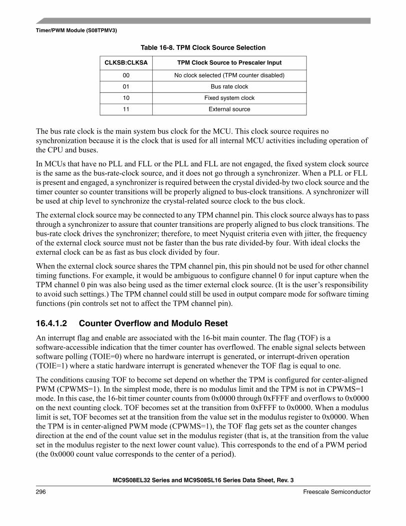
Timer/PWM Module (S08TPMV3)
MC9S08EL32 Series and MC9S08SL16 Series Data Sheet, Rev. 3
296 Freescale Semiconductor
The bus rate clock is the main system bus clock for the MCU. This clock source requires no synchronization because it is the clock that is used for all internal MCU activities including operation of the CPU and buses.
In MCUs that have no PLL and FLL or the PLL and FLL are not engaged, the fixed system clock source is the same as the bus-rate-clock source, and it does not go through a synchronizer. When a PLL or FLL is present and engaged, a synchronizer is required between the crystal divided-by two clock source and the timer counter so counter transitions will be properly aligned to bus-clock transitions. A synchronizer will be used at chip level to synchronize the crystal-related source clock to the bus clock.
The external clock source may be connected to any TPM channel pin. This clock source always has to pass through a synchronizer to assure that counter transitions are properly aligned to bus clock transitions. The bus-rate clock drives the synchronizer; therefore, to meet Nyquist criteria even with jitter, the frequency of the external clock source must not be faster than the bus rate divided-by four. With ideal clocks the external clock can be as fast as bus clock divided by four.
When the external clock source shares the TPM channel pin, this pin should not be used for other channel timing functions. For example, it would be ambiguous to configure channel 0 for input capture when the TPM channel 0 pin was also being used as the timer external clock source. (It is the user’s responsibility to avoid such settings.) The TPM channel could still be used in output compare mode for software timing functions (pin controls set not to affect the TPM channel pin).
16.4.1.2 Counter Overflow and Modulo Reset
An interrupt flag and enable are associated with the 16-bit main counter. The flag (TOF) is a software-accessible indication that the timer counter has overflowed. The enable signal selects between software polling (TOIE=0) where no hardware interrupt is generated, or interrupt-driven operation (TOIE=1) where a static hardware interrupt is generated whenever the TOF flag is equal to one.
The conditions causing TOF to become set depend on whether the TPM is configured for center-aligned PWM (CPWMS=1). In the simplest mode, there is no modulus limit and the TPM is not in CPWMS=1 mode. In this case, the 16-bit timer counter counts from 0x0000 through 0xFFFF and overflows to 0x0000 on the next counting clock. TOF becomes set at the transition from 0xFFFF to 0x0000. When a modulus limit is set, TOF becomes set at the transition from the value set in the modulus register to 0x0000. When the TPM is in center-aligned PWM mode (CPWMS=1), the TOF flag gets set as the counter changes direction at the end of the count value set in the modulus register (that is, at the transition from the value set in the modulus register to the next lower count value). This corresponds to the end of a PWM period (the 0x0000 count value corresponds to the center of a period).
Table 16-8. TPM Clock Source Selection
CLKSB:CLKSA TPM Clock Source to Prescaler Input
00 No clock selected (TPM counter disabled)
01 Bus rate clock
10 Fixed system clock
11 External source
Timer/PWM Module (S08TPMV3)
MC9S08EL32 Series and MC9S08SL16 Series Data Sheet, Rev. 3
Freescale Semiconductor 297
16.4.1.3 Counting Modes
The main timer counter has two counting modes. When center-aligned PWM is selected (CPWMS=1), the counter operates in up/down counting mode. Otherwise, the counter operates as a simple up counter. As an up counter, the timer counter counts from 0x0000 through its terminal count and then continues with 0x0000. The terminal count is 0xFFFF or a modulus value in TPMxMODH:TPMxMODL.
When center-aligned PWM operation is specified, the counter counts up from 0x0000 through its terminal count and then down to 0x0000 where it changes back to up counting. Both 0x0000 and the terminal count value are normal length counts (one timer clock period long). In this mode, the timer overflow flag (TOF) becomes set at the end of the terminal-count period (as the count changes to the next lower count value).
16.4.1.4 Manual Counter Reset
The main timer counter can be manually reset at any time by writing any value to either half of TPMxCNTH or TPMxCNTL. Resetting the counter in this manner also resets the coherency mechanism in case only half of the counter was read before resetting the count.
16.4.2 Channel Mode Selection
Provided CPWMS=0, the MSnB and MSnA control bits in the channel n status and control registers determine the basic mode of operation for the corresponding channel. Choices include input capture, output compare, and edge-aligned PWM.
16.4.2.1 Input Capture Mode
With the input-capture function, the TPM can capture the time at which an external event occurs. When an active edge occurs on the pin of an input-capture channel, the TPM latches the contents of the TPM counter into the channel-value registers (TPMxCnVH:TPMxCnVL). Rising edges, falling edges, or any edge may be chosen as the active edge that triggers an input capture.
In input capture mode, the TPMxCnVH and TPMxCnVL registers are read only.
When either half of the 16-bit capture register is read, the other half is latched into a buffer to support coherent 16-bit accesses in big-endian or little-endian order. The coherency sequence can be manually reset by writing to the channel status/control register (TPMxCnSC).
An input capture event sets a flag bit (CHnF) which may optionally generate a CPU interrupt request.
While in BDM, the input capture function works as configured by the user. When an external event occurs, the TPM latches the contents of the TPM counter (which is frozen because of the BDM mode) into the channel value registers and sets the flag bit.
16.4.2.2 Output Compare Mode
With the output-compare function, the TPM can generate timed pulses with programmable position, polarity, duration, and frequency. When the counter reaches the value in the channel-value registers of an output-compare channel, the TPM can set, clear, or toggle the channel pin.
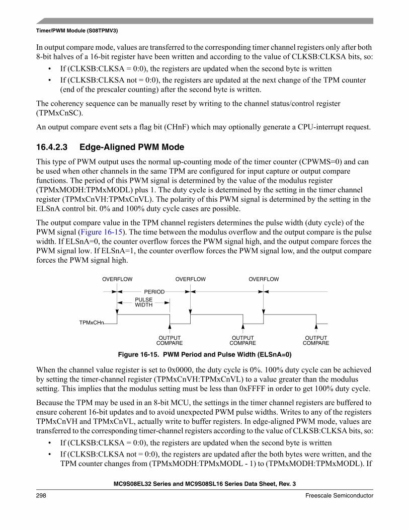
Timer/PWM Module (S08TPMV3)
MC9S08EL32 Series and MC9S08SL16 Series Data Sheet, Rev. 3
298 Freescale Semiconductor
In output compare mode, values are transferred to the corresponding timer channel registers only after both 8-bit halves of a 16-bit register have been written and according to the value of CLKSB:CLKSA bits, so:
• If (CLKSB:CLKSA = 0:0), the registers are updated when the second byte is written• If (CLKSB:CLKSA not = 0:0), the registers are updated at the next change of the TPM counter
(end of the prescaler counting) after the second byte is written.
The coherency sequence can be manually reset by writing to the channel status/control register (TPMxCnSC).
An output compare event sets a flag bit (CHnF) which may optionally generate a CPU-interrupt request.
16.4.2.3 Edge-Aligned PWM Mode
This type of PWM output uses the normal up-counting mode of the timer counter (CPWMS=0) and can be used when other channels in the same TPM are configured for input capture or output compare functions. The period of this PWM signal is determined by the value of the modulus register (TPMxMODH:TPMxMODL) plus 1. The duty cycle is determined by the setting in the timer channel register (TPMxCnVH:TPMxCnVL). The polarity of this PWM signal is determined by the setting in the ELSnA control bit. 0% and 100% duty cycle cases are possible.
The output compare value in the TPM channel registers determines the pulse width (duty cycle) of the PWM signal (Figure 16-15). The time between the modulus overflow and the output compare is the pulse width. If ELSnA=0, the counter overflow forces the PWM signal high, and the output compare forces the PWM signal low. If ELSnA=1, the counter overflow forces the PWM signal low, and the output compare forces the PWM signal high.
Figure 16-15. PWM Period and Pulse Width (ELSnA=0)
When the channel value register is set to 0x0000, the duty cycle is 0%. 100% duty cycle can be achieved by setting the timer-channel register (TPMxCnVH:TPMxCnVL) to a value greater than the modulus setting. This implies that the modulus setting must be less than 0xFFFF in order to get 100% duty cycle.
Because the TPM may be used in an 8-bit MCU, the settings in the timer channel registers are buffered to ensure coherent 16-bit updates and to avoid unexpected PWM pulse widths. Writes to any of the registers TPMxCnVH and TPMxCnVL, actually write to buffer registers. In edge-aligned PWM mode, values are transferred to the corresponding timer-channel registers according to the value of CLKSB:CLKSA bits, so:
• If (CLKSB:CLKSA = 0:0), the registers are updated when the second byte is written• If (CLKSB:CLKSA not = 0:0), the registers are updated after the both bytes were written, and the
TPM counter changes from (TPMxMODH:TPMxMODL - 1) to (TPMxMODH:TPMxMODL). If
PERIOD
PULSEWIDTH
OVERFLOW OVERFLOW OVERFLOW
OUTPUTCOMPARE
OUTPUTCOMPARE
OUTPUTCOMPARE
TPMxCHn
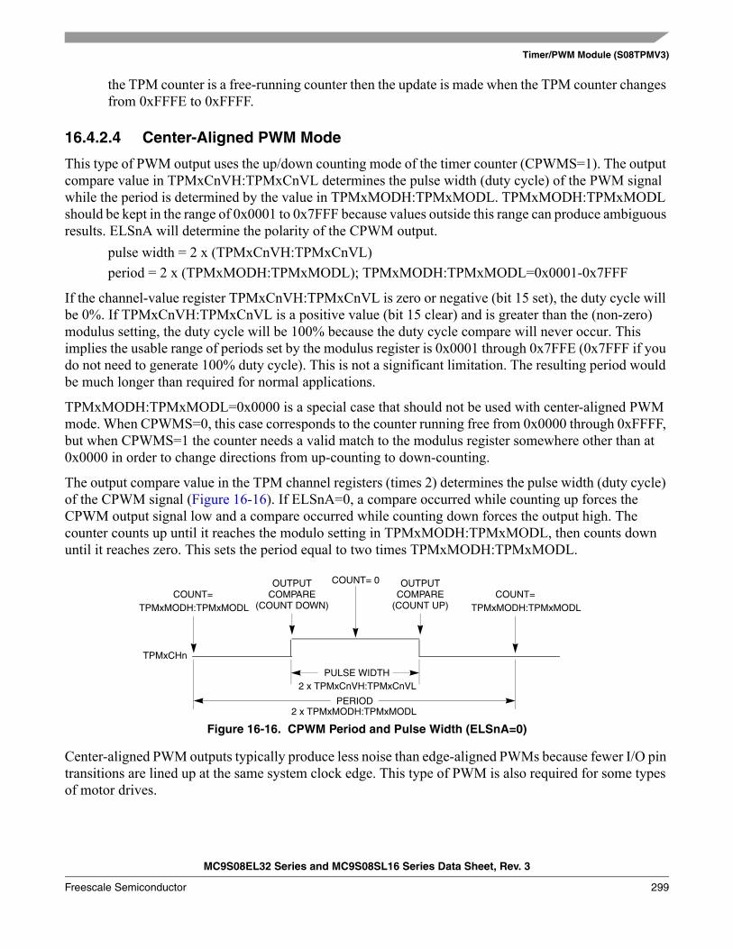
Timer/PWM Module (S08TPMV3)
MC9S08EL32 Series and MC9S08SL16 Series Data Sheet, Rev. 3
Freescale Semiconductor 299
the TPM counter is a free-running counter then the update is made when the TPM counter changes from 0xFFFE to 0xFFFF.
16.4.2.4 Center-Aligned PWM Mode
This type of PWM output uses the up/down counting mode of the timer counter (CPWMS=1). The output compare value in TPMxCnVH:TPMxCnVL determines the pulse width (duty cycle) of the PWM signal while the period is determined by the value in TPMxMODH:TPMxMODL. TPMxMODH:TPMxMODL should be kept in the range of 0x0001 to 0x7FFF because values outside this range can produce ambiguous results. ELSnA will determine the polarity of the CPWM output.
pulse width = 2 x (TPMxCnVH:TPMxCnVL)period = 2 x (TPMxMODH:TPMxMODL); TPMxMODH:TPMxMODL=0x0001-0x7FFF
If the channel-value register TPMxCnVH:TPMxCnVL is zero or negative (bit 15 set), the duty cycle will be 0%. If TPMxCnVH:TPMxCnVL is a positive value (bit 15 clear) and is greater than the (non-zero) modulus setting, the duty cycle will be 100% because the duty cycle compare will never occur. This implies the usable range of periods set by the modulus register is 0x0001 through 0x7FFE (0x7FFF if you do not need to generate 100% duty cycle). This is not a significant limitation. The resulting period would be much longer than required for normal applications.
TPMxMODH:TPMxMODL=0x0000 is a special case that should not be used with center-aligned PWM mode. When CPWMS=0, this case corresponds to the counter running free from 0x0000 through 0xFFFF, but when CPWMS=1 the counter needs a valid match to the modulus register somewhere other than at 0x0000 in order to change directions from up-counting to down-counting.
The output compare value in the TPM channel registers (times 2) determines the pulse width (duty cycle) of the CPWM signal (Figure 16-16). If ELSnA=0, a compare occurred while counting up forces the CPWM output signal low and a compare occurred while counting down forces the output high. The counter counts up until it reaches the modulo setting in TPMxMODH:TPMxMODL, then counts down until it reaches zero. This sets the period equal to two times TPMxMODH:TPMxMODL.
Figure 16-16. CPWM Period and Pulse Width (ELSnA=0)
Center-aligned PWM outputs typically produce less noise than edge-aligned PWMs because fewer I/O pin transitions are lined up at the same system clock edge. This type of PWM is also required for some types of motor drives.
PERIOD
PULSE WIDTH
COUNT=
COUNT= 0
COUNT=OUTPUT
COMPARE(COUNT DOWN)
OUTPUTCOMPARE
(COUNT UP)
TPMxCHn
2 x TPMxMODH:TPMxMODL
2 x TPMxCnVH:TPMxCnVL
TPMxMODH:TPMxMODLTPMxMODH:TPMxMODL
Timer/PWM Module (S08TPMV3)
MC9S08EL32 Series and MC9S08SL16 Series Data Sheet, Rev. 3
300 Freescale Semiconductor
Input capture, output compare, and edge-aligned PWM functions do not make sense when the counter is operating in up/down counting mode so this implies that all active channels within a TPM must be used in CPWM mode when CPWMS=1.
The TPM may be used in an 8-bit MCU. The settings in the timer channel registers are buffered to ensure coherent 16-bit updates and to avoid unexpected PWM pulse widths. Writes to any of the registers TPMxMODH, TPMxMODL, TPMxCnVH, and TPMxCnVL, actually write to buffer registers.
In center-aligned PWM mode, the TPMxCnVH:L registers are updated with the value of their write buffer according to the value of CLKSB:CLKSA bits, so:
• If (CLKSB:CLKSA = 0:0), the registers are updated when the second byte is written• If (CLKSB:CLKSA not = 0:0), the registers are updated after the both bytes were written, and the
TPM counter changes from (TPMxMODH:TPMxMODL - 1) to (TPMxMODH:TPMxMODL). If the TPM counter is a free-running counter, the update is made when the TPM counter changes from 0xFFFE to 0xFFFF.
When TPMxCNTH:TPMxCNTL=TPMxMODH:TPMxMODL, the TPM can optionally generate a TOF interrupt (at the end of this count).
Writing to TPMxSC cancels any values written to TPMxMODH and/or TPMxMODL and resets the coherency mechanism for the modulo registers. Writing to TPMxCnSC cancels any values written to the channel value registers and resets the coherency mechanism for TPMxCnVH:TPMxCnVL.
16.5 Reset Overview
16.5.1 General
The TPM is reset whenever any MCU reset occurs.
16.5.2 Description of Reset Operation
Reset clears the TPMxSC register which disables clocks to the TPM and disables timer overflow interrupts (TOIE=0). CPWMS, MSnB, MSnA, ELSnB, and ELSnA are all cleared which configures all TPM channels for input-capture operation with the associated pins disconnected from I/O pin logic (so all MCU pins related to the TPM revert to general purpose I/O pins).
16.6 Interrupts
16.6.1 General
The TPM generates an optional interrupt for the main counter overflow and an interrupt for each channel. The meaning of channel interrupts depends on each channel’s mode of operation. If the channel is configured for input capture, the interrupt flag is set each time the selected input capture edge is recognized. If the channel is configured for output compare or PWM modes, the interrupt flag is set each time the main timer counter matches the value in the 16-bit channel value register.
Timer/PWM Module (S08TPMV3)
MC9S08EL32 Series and MC9S08SL16 Series Data Sheet, Rev. 3
Freescale Semiconductor 301
All TPM interrupts are listed in Table 16-9 which shows the interrupt name, the name of any local enable that can block the interrupt request from leaving the TPM and getting recognized by the separate interrupt processing logic.
The TPM module will provide a high-true interrupt signal. Vectors and priorities are determined at chip integration time in the interrupt module so refer to the user’s guide for the interrupt module or to the chip’s complete documentation for details.
16.6.2 Description of Interrupt Operation
For each interrupt source in the TPM, a flag bit is set upon recognition of the interrupt condition such as timer overflow, channel-input capture, or output-compare events. This flag may be read (polled) by software to determine that the action has occurred, or an associated enable bit (TOIE or CHnIE) can be set to enable hardware interrupt generation. While the interrupt enable bit is set, a static interrupt will generate whenever the associated interrupt flag equals one. The user’s software must perform a sequence of steps to clear the interrupt flag before returning from the interrupt-service routine.
TPM interrupt flags are cleared by a two-step process including a read of the flag bit while it is set (1) followed by a write of zero (0) to the bit. If a new event is detected between these two steps, the sequence is reset and the interrupt flag remains set after the second step to avoid the possibility of missing the new event.
16.6.2.1 Timer Overflow Interrupt (TOF) Description
The meaning and details of operation for TOF interrupts varies slightly depending upon the mode of operation of the TPM system (general purpose timing functions versus center-aligned PWM operation). The flag is cleared by the two step sequence described above.
16.6.2.1.1 Normal Case
Normally TOF is set when the timer counter changes from 0xFFFF to 0x0000. When the TPM is not configured for center-aligned PWM (CPWMS=0), TOF gets set when the timer counter changes from the terminal count (the value in the modulo register) to 0x0000. This case corresponds to the normal meaning of counter overflow.
Table 16-9. Interrupt Summary
InterruptLocal
EnableSource Description
TOF TOIE Counter overflow Set each time the timer counter reaches its terminal count (at transition to next count value which is usually 0x0000)
CHnF CHnIE Channel event An input capture or output compare event took place on channel n
Timer/PWM Module (S08TPMV3)
MC9S08EL32 Series and MC9S08SL16 Series Data Sheet, Rev. 3
302 Freescale Semiconductor
16.6.2.1.2 Center-Aligned PWM Case
When CPWMS=1, TOF gets set when the timer counter changes direction from up-counting to down-counting at the end of the terminal count (the value in the modulo register). In this case the TOF corresponds to the end of a PWM period.
16.6.2.2 Channel Event Interrupt Description
The meaning of channel interrupts depends on the channel’s current mode (input-capture, output-compare, edge-aligned PWM, or center-aligned PWM).
16.6.2.2.1 Input Capture Events
When a channel is configured as an input capture channel, the ELSnB:ELSnA control bits select no edge (off), rising edges, falling edges or any edge as the edge which triggers an input capture event. When the selected edge is detected, the interrupt flag is set. The flag is cleared by the two-step sequence described in Section 16.6.2, “Description of Interrupt Operation.”
16.6.2.2.2 Output Compare Events
When a channel is configured as an output compare channel, the interrupt flag is set each time the main timer counter matches the 16-bit value in the channel value register. The flag is cleared by the two-step sequence described Section 16.6.2, “Description of Interrupt Operation.”
16.6.2.2.3 PWM End-of-Duty-Cycle Events
For channels configured for PWM operation there are two possibilities. When the channel is configured for edge-aligned PWM, the channel flag gets set when the timer counter matches the channel value register which marks the end of the active duty cycle period. When the channel is configured for center-aligned PWM, the timer count matches the channel value register twice during each PWM cycle. In this CPWM case, the channel flag is set at the start and at the end of the active duty cycle period which are the times when the timer counter matches the channel value register. The flag is cleared by the two-step sequence described Section 16.6.2, “Description of Interrupt Operation.”
16.7 The Differences from TPM v2 to TPM v31. Write to TPMxCNTH:L registers (Section 16.3.2, “TPM-Counter Registers
(TPMxCNTH:TPMxCNTL)) [SE110-TPM case 7]Any write to TPMxCNTH or TPMxCNTL registers in TPM v3 clears the TPM counter (TPMxCNTH:L) and the prescaler counter. Instead, in the TPM v2 only the TPM counter is cleared in this case.
2. Read of TPMxCNTH:L registers (Section 16.3.2, “TPM-Counter Registers (TPMxCNTH:TPMxCNTL))— In TPM v3, any read of TPMxCNTH:L registers during BDM mode returns the value of the
TPM counter that is frozen. In TPM v2, if only one byte of the TPMxCNTH:L registers was read before the BDM mode became active, then any read of TPMxCNTH:L registers during
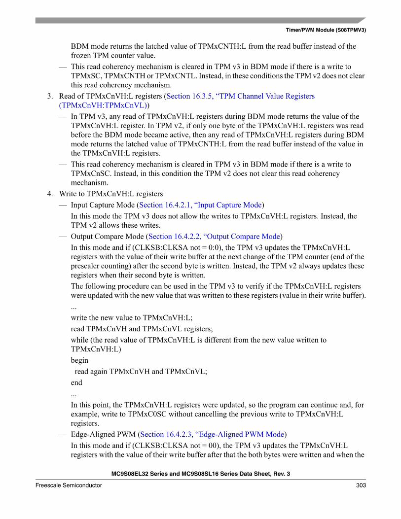
Timer/PWM Module (S08TPMV3)
MC9S08EL32 Series and MC9S08SL16 Series Data Sheet, Rev. 3
Freescale Semiconductor 303
BDM mode returns the latched value of TPMxCNTH:L from the read buffer instead of the frozen TPM counter value.
— This read coherency mechanism is cleared in TPM v3 in BDM mode if there is a write to TPMxSC, TPMxCNTH or TPMxCNTL. Instead, in these conditions the TPM v2 does not clear this read coherency mechanism.
3. Read of TPMxCnVH:L registers (Section 16.3.5, “TPM Channel Value Registers (TPMxCnVH:TPMxCnVL))— In TPM v3, any read of TPMxCnVH:L registers during BDM mode returns the value of the
TPMxCnVH:L register. In TPM v2, if only one byte of the TPMxCnVH:L registers was read before the BDM mode became active, then any read of TPMxCnVH:L registers during BDM mode returns the latched value of TPMxCNTH:L from the read buffer instead of the value in the TPMxCnVH:L registers.
— This read coherency mechanism is cleared in TPM v3 in BDM mode if there is a write to TPMxCnSC. Instead, in this condition the TPM v2 does not clear this read coherency mechanism.
4. Write to TPMxCnVH:L registers— Input Capture Mode (Section 16.4.2.1, “Input Capture Mode)
In this mode the TPM v3 does not allow the writes to TPMxCnVH:L registers. Instead, the TPM v2 allows these writes.
— Output Compare Mode (Section 16.4.2.2, “Output Compare Mode)In this mode and if (CLKSB:CLKSA not = 0:0), the TPM v3 updates the TPMxCnVH:L registers with the value of their write buffer at the next change of the TPM counter (end of the prescaler counting) after the second byte is written. Instead, the TPM v2 always updates these registers when their second byte is written.The following procedure can be used in the TPM v3 to verify if the TPMxCnVH:L registers were updated with the new value that was written to these registers (value in their write buffer)....write the new value to TPMxCnVH:L;read TPMxCnVH and TPMxCnVL registers;while (the read value of TPMxCnVH:L is different from the new value written to TPMxCnVH:L)begin read again TPMxCnVH and TPMxCnVL;end...In this point, the TPMxCnVH:L registers were updated, so the program can continue and, for example, write to TPMxC0SC without cancelling the previous write to TPMxCnVH:L registers.
— Edge-Aligned PWM (Section 16.4.2.3, “Edge-Aligned PWM Mode)In this mode and if (CLKSB:CLKSA not = 00), the TPM v3 updates the TPMxCnVH:L registers with the value of their write buffer after that the both bytes were written and when the
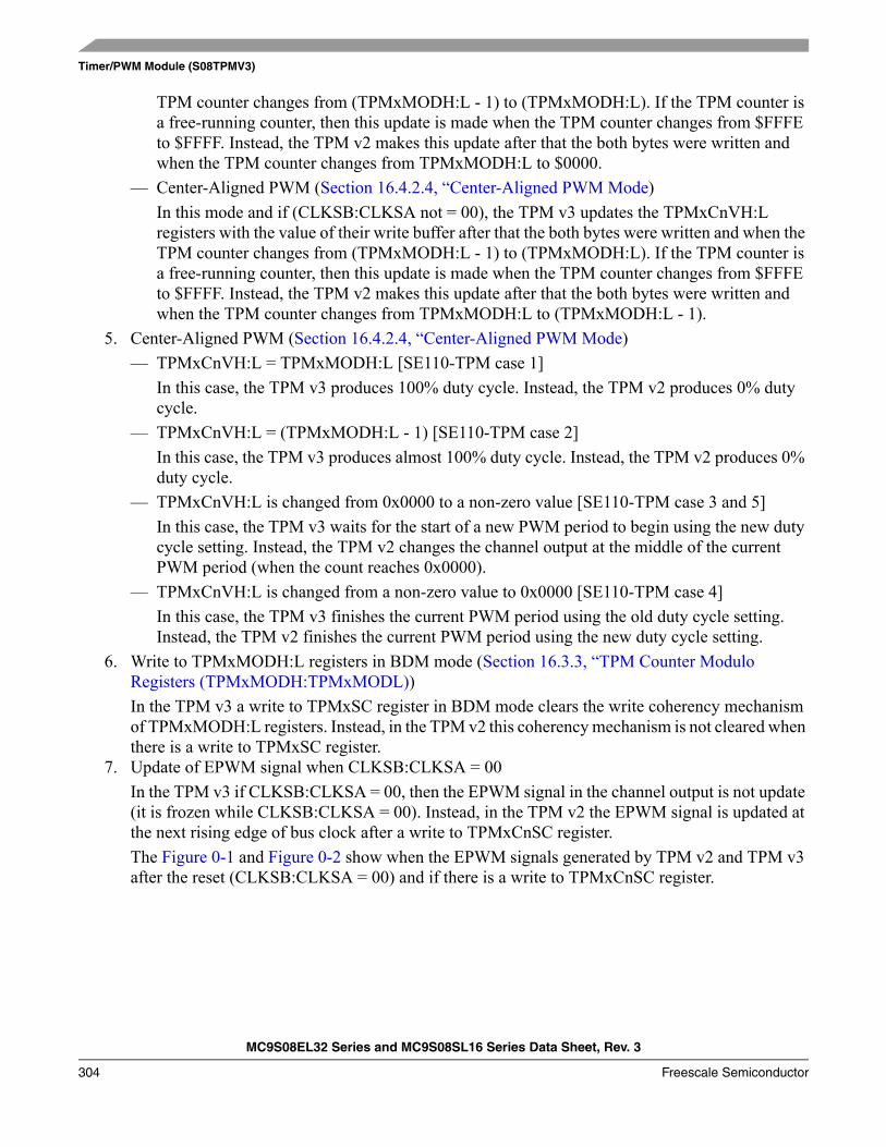
Timer/PWM Module (S08TPMV3)
MC9S08EL32 Series and MC9S08SL16 Series Data Sheet, Rev. 3
304 Freescale Semiconductor
TPM counter changes from (TPMxMODH:L - 1) to (TPMxMODH:L). If the TPM counter is a free-running counter, then this update is made when the TPM counter changes from $FFFE to $FFFF. Instead, the TPM v2 makes this update after that the both bytes were written and when the TPM counter changes from TPMxMODH:L to $0000.
— Center-Aligned PWM (Section 16.4.2.4, “Center-Aligned PWM Mode)In this mode and if (CLKSB:CLKSA not = 00), the TPM v3 updates the TPMxCnVH:L registers with the value of their write buffer after that the both bytes were written and when the TPM counter changes from (TPMxMODH:L - 1) to (TPMxMODH:L). If the TPM counter is a free-running counter, then this update is made when the TPM counter changes from $FFFE to $FFFF. Instead, the TPM v2 makes this update after that the both bytes were written and when the TPM counter changes from TPMxMODH:L to (TPMxMODH:L - 1).
5. Center-Aligned PWM (Section 16.4.2.4, “Center-Aligned PWM Mode)— TPMxCnVH:L = TPMxMODH:L [SE110-TPM case 1]
In this case, the TPM v3 produces 100% duty cycle. Instead, the TPM v2 produces 0% duty cycle.
— TPMxCnVH:L = (TPMxMODH:L - 1) [SE110-TPM case 2]In this case, the TPM v3 produces almost 100% duty cycle. Instead, the TPM v2 produces 0% duty cycle.
— TPMxCnVH:L is changed from 0x0000 to a non-zero value [SE110-TPM case 3 and 5]In this case, the TPM v3 waits for the start of a new PWM period to begin using the new duty cycle setting. Instead, the TPM v2 changes the channel output at the middle of the current PWM period (when the count reaches 0x0000).
— TPMxCnVH:L is changed from a non-zero value to 0x0000 [SE110-TPM case 4]In this case, the TPM v3 finishes the current PWM period using the old duty cycle setting. Instead, the TPM v2 finishes the current PWM period using the new duty cycle setting.
6. Write to TPMxMODH:L registers in BDM mode (Section 16.3.3, “TPM Counter Modulo Registers (TPMxMODH:TPMxMODL))In the TPM v3 a write to TPMxSC register in BDM mode clears the write coherency mechanism of TPMxMODH:L registers. Instead, in the TPM v2 this coherency mechanism is not cleared when there is a write to TPMxSC register.
7. Update of EPWM signal when CLKSB:CLKSA = 00In the TPM v3 if CLKSB:CLKSA = 00, then the EPWM signal in the channel output is not update (it is frozen while CLKSB:CLKSA = 00). Instead, in the TPM v2 the EPWM signal is updated at the next rising edge of bus clock after a write to TPMxCnSC register.The Figure 0-1 and Figure 0-2 show when the EPWM signals generated by TPM v2 and TPM v3 after the reset (CLKSB:CLKSA = 00) and if there is a write to TPMxCnSC register.
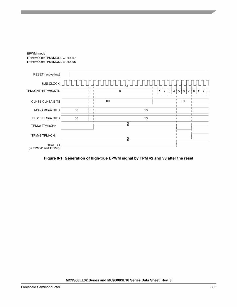
MC9S08EL32 Series and MC9S08SL16 Series Data Sheet, Rev. 3
Freescale Semiconductor 305
Figure 0-1. Generation of high-true EPWM signal by TPM v2 and v3 after the reset
ELSnB:ELSnA BITS
CLKSB:CLKSA BITS
0
TPMxMODH:TPMxMODL = 0x0007TPMxMODH:TPMxMODL = 0x0005
TPMxCNTH:TPMxCNTL
TPMv2 TPMxCHn
EPWM mode
00
00 10
BUS CLOCK
01
1 2 3 4 5 6 7 0 1 2
CHnF BIT
MSnB:MSnA BITS 00 10
(in TPMv2 and TPMv3)
TPMv3 TPMxCHn
...
RESET (active low)
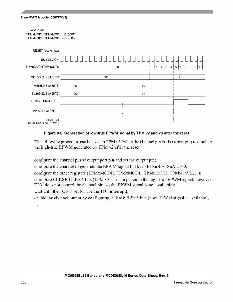
Timer/PWM Module (S08TPMV3)
MC9S08EL32 Series and MC9S08SL16 Series Data Sheet, Rev. 3
306 Freescale Semiconductor
Figure 0-2. Generation of low-true EPWM signal by TPM v2 and v3 after the reset
The following procedure can be used in TPM v3 (when the channel pin is also a port pin) to emulate the high-true EPWM generated by TPM v2 after the reset....configure the channel pin as output port pin and set the output pin;configure the channel to generate the EPWM signal but keep ELSnB:ELSnA as 00;configure the other registers (TPMxMODH, TPMxMODL, TPMxCnVH, TPMxCnVL, ...);configure CLKSB:CLKSA bits (TPM v3 starts to generate the high-true EPWM signal, however TPM does not control the channel pin, so the EPWM signal is not available);wait until the TOF is set (or use the TOF interrupt);enable the channel output by configuring ELSnB:ELSnA bits (now EPWM signal is available);...
ELSnB:ELSnA BITS
CLKSB:CLKSA BITS
0
TPMxMODH:TPMxMODL = 0x0007TPMxMODH:TPMxMODL = 0x0005
TPMxCNTH:TPMxCNTL
TPMv2 TPMxCHn
EPWM mode
00
00 01
BUS CLOCK
01
1 2 3 4 5 6 7 0 1 2
CHnF BIT
MSnB:MSnA BITS 00 10
(in TPMv2 and TPMv3)
TPMv3 TPMxCHn
...
RESET (active low)
MC9S08EL32 Series and MC9S08SL16 Series Data Sheet, Rev. 3
Freescale Semiconductor 307
Chapter 17 Development Support
17.1 IntroductionDevelopment support systems in the HCS08 include the background debug controller (BDC) and the on-chip debug module (DBG). The BDC provides a single-wire debug interface to the target MCU that provides a convenient interface for programming the on-chip FLASH and other nonvolatile memories. The BDC is also the primary debug interface for development and allows non-intrusive access to memory data and traditional debug features such as CPU register modify, breakpoints, and single instruction trace commands.
In the HCS08 Family, address and data bus signals are not available on external pins (not even in test modes). Debug is done through commands fed into the target MCU via the single-wire background debug interface. The debug module provides a means to selectively trigger and capture bus information so an external development system can reconstruct what happened inside the MCU on a cycle-by-cycle basis without having external access to the address and data signals.
17.1.1 Forcing Active Background
The method for forcing active background mode depends on the specific HCS08 derivative. For the MC9S08EL32 Series and MC9S08SL16 Series, you can force active background after a power-on reset by holding the BKGD pin low as the device exits the reset condition (independent of the reset source). You can also force active background by driving BKGD low immediately after a serial background command that writes a one to the BDFR bit in the SBDFR register. If no debug pod is connected to the BKGD pin, the MCU always resets into normal operating mode.
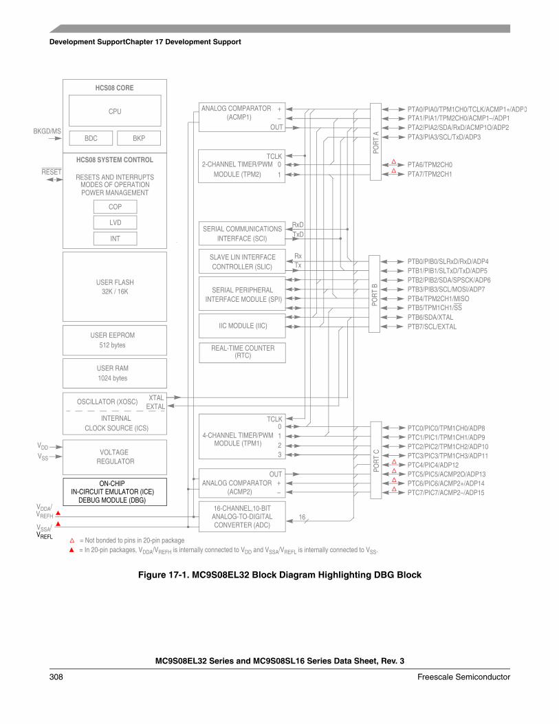
Development SupportChapter 17 Development Support
MC9S08EL32 Series and MC9S08SL16 Series Data Sheet, Rev. 3
308 Freescale Semiconductor
Figure 17-1. MC9S08EL32 Block Diagram Highlighting DBG Block
VSS
IIC MODULE (IIC)
SERIAL PERIPHERAL INTERFACE MODULE (SPI)
USER FLASH
USER RAM
32K / 16K
HCS08 CORE
CPU
BDC
2-CHANNEL TIMER/PWMMODULE (TPM2)
HCS08 SYSTEM CONTROL
RESETS AND INTERRUPTSMODES OF OPERATIONPOWER MANAGEMENT
VOLTAGE REGULATOR
COP
LVD
OSCILLATOR (XOSC)
INTERNALCLOCK SOURCE (ICS)
RESET
VREFH
1024 bytes
INTERFACE (SCI)SERIAL COMMUNICATIONS
XTALEXTAL
4-CHANNEL TIMER/PWMMODULE (TPM1)
REAL-TIME COUNTER
IN-CIRCUIT EMULATOR (ICE)
BKGD/MS PTA3/PIA3/SCL/TxD/ADP3
PTA6/TPM2CH0
PTA2/PIA2/SDA/RxD/ACMP1O/ADP2PTA1/PIA1/TPM2CH0/ACMP1–/ADP1PTA0/PIA0/TPM1CH0/TCLK/ACMP1+/ADP0
PTA7/TPM2CH1
PTB3/PIB3/SCL/MOSI/ADP7PTB4/TPM2CH1/MISO
PTB2/PIB2/SDA/SPSCK/ADP6PTB1/PIB1/SLTxD/TxD/ADP5PTB0/PIB0/SLRxD/RxD/ADP4
PTB7/SCL/EXTAL
PTC3/PIC3/TPM1CH3/ADP11PTC4/PIC4/ADP12PTC5/PIC5/ACMP2O/ADP13
PTC2/PIC2/TPM1CH2/ADP10PTC1/PIC1/TPM1CH1/ADP9
POR
T C
PTC6/PIC6/ACMP2+/ADP14
VDD
BKP
INT
ANALOG COMPARATOR(ACMP2)
USER EEPROM512 bytes
CONTROLLER (SLIC)SLAVE LIN INTERFACE
ANALOG-TO-DIGITALCONVERTER (ADC)
16-CHANNEL,10-BIT16
= In 20-pin packages, VDDA/VREFH is internally connected to VDD and VSSA/VREFL is internally connected to VSS.
VDDA/
VREFL
VSSA/
DEBUG MODULE (DBG)
ON-CHIP
(RTC)
PTC0/PIC0/TPM1CH0/ADP8
PTC7/PIC7/ACMP2–/ADP15
PTB6/SDA/XTAL
POR
T B
POR
T A
PTB5/TPM1CH1/SS
ANALOG COMPARATOR(ACMP1)
= Not bonded to pins in 20-pin package
TCLK
TCLK
+–
OUT
+–
OUT
0123
10
RxDTxD
TxRx

Development SupportChapter 17 Development Support
MC9S08EL32 Series and MC9S08SL16 Series Data Sheet, Rev. 3
Freescale Semiconductor 309
Development Support
MC9S08EL32 Series and MC9S08SL16 Series Data Sheet, Rev. 3
310 Freescale Semiconductor
17.1.2 Features
Features of the BDC module include:• Single pin for mode selection and background communications• BDC registers are not located in the memory map• SYNC command to determine target communications rate• Non-intrusive commands for memory access• Active background mode commands for CPU register access• GO and TRACE1 commands• BACKGROUND command can wake CPU from stop or wait modes• One hardware address breakpoint built into BDC• Oscillator runs in stop mode, if BDC enabled• COP watchdog disabled while in active background mode
Features of the ICE system include:• Two trigger comparators: Two address + read/write (R/W) or one full address + data + R/W• Flexible 8-word by 16-bit FIFO (first-in, first-out) buffer for capture information:
— Change-of-flow addresses or— Event-only data
• Two types of breakpoints:— Tag breakpoints for instruction opcodes— Force breakpoints for any address access
• Nine trigger modes:— Basic: A-only, A OR B— Sequence: A then B— Full: A AND B data, A AND NOT B data — Event (store data): Event-only B, A then event-only B— Range: Inside range (A ≤ address ≤ B), outside range (address < A or address > B)
17.2 Background Debug Controller (BDC)All MCUs in the HCS08 Family contain a single-wire background debug interface that supports in-circuit programming of on-chip nonvolatile memory and sophisticated non-intrusive debug capabilities. Unlike debug interfaces on earlier 8-bit MCUs, this system does not interfere with normal application resources. It does not use any user memory or locations in the memory map and does not share any on-chip peripherals.
BDC commands are divided into two groups:• Active background mode commands require that the target MCU is in active background mode (the
user program is not running). Active background mode commands allow the CPU registers to be read or written, and allow the user to trace one user instruction at a time, or GO to the user program from active background mode.
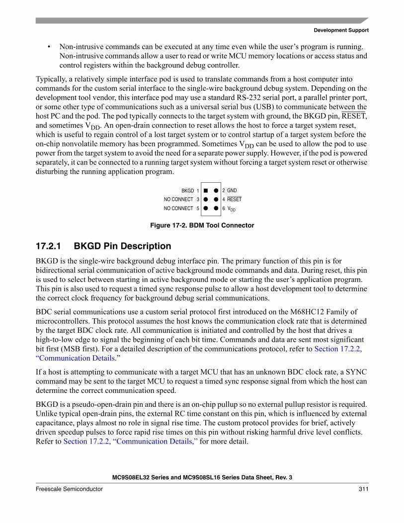
Development Support
MC9S08EL32 Series and MC9S08SL16 Series Data Sheet, Rev. 3
Freescale Semiconductor 311
• Non-intrusive commands can be executed at any time even while the user’s program is running. Non-intrusive commands allow a user to read or write MCU memory locations or access status and control registers within the background debug controller.
Typically, a relatively simple interface pod is used to translate commands from a host computer into commands for the custom serial interface to the single-wire background debug system. Depending on the development tool vendor, this interface pod may use a standard RS-232 serial port, a parallel printer port, or some other type of communications such as a universal serial bus (USB) to communicate between the host PC and the pod. The pod typically connects to the target system with ground, the BKGD pin, RESET, and sometimes VDD. An open-drain connection to reset allows the host to force a target system reset, which is useful to regain control of a lost target system or to control startup of a target system before the on-chip nonvolatile memory has been programmed. Sometimes VDD can be used to allow the pod to use power from the target system to avoid the need for a separate power supply. However, if the pod is powered separately, it can be connected to a running target system without forcing a target system reset or otherwise disturbing the running application program.
Figure 17-2. BDM Tool Connector
17.2.1 BKGD Pin Description
BKGD is the single-wire background debug interface pin. The primary function of this pin is for bidirectional serial communication of active background mode commands and data. During reset, this pin is used to select between starting in active background mode or starting the user’s application program. This pin is also used to request a timed sync response pulse to allow a host development tool to determine the correct clock frequency for background debug serial communications.
BDC serial communications use a custom serial protocol first introduced on the M68HC12 Family of microcontrollers. This protocol assumes the host knows the communication clock rate that is determined by the target BDC clock rate. All communication is initiated and controlled by the host that drives a high-to-low edge to signal the beginning of each bit time. Commands and data are sent most significant bit first (MSB first). For a detailed description of the communications protocol, refer to Section 17.2.2, “Communication Details.”
If a host is attempting to communicate with a target MCU that has an unknown BDC clock rate, a SYNC command may be sent to the target MCU to request a timed sync response signal from which the host can determine the correct communication speed.
BKGD is a pseudo-open-drain pin and there is an on-chip pullup so no external pullup resistor is required. Unlike typical open-drain pins, the external RC time constant on this pin, which is influenced by external capacitance, plays almost no role in signal rise time. The custom protocol provides for brief, actively driven speedup pulses to force rapid rise times on this pin without risking harmful drive level conflicts. Refer to Section 17.2.2, “Communication Details,” for more detail.
2
4
6NO CONNECT 5
NO CONNECT 3
1
RESET
BKGD GND
VDD
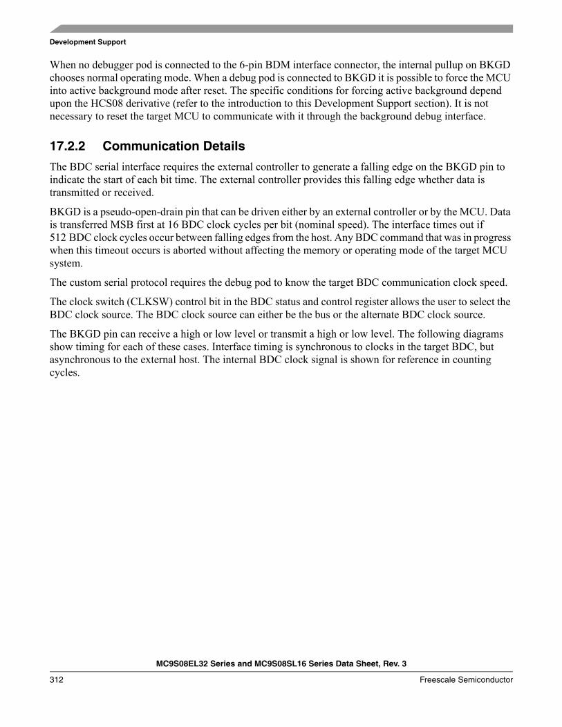
Development Support
MC9S08EL32 Series and MC9S08SL16 Series Data Sheet, Rev. 3
312 Freescale Semiconductor
When no debugger pod is connected to the 6-pin BDM interface connector, the internal pullup on BKGD chooses normal operating mode. When a debug pod is connected to BKGD it is possible to force the MCU into active background mode after reset. The specific conditions for forcing active background depend upon the HCS08 derivative (refer to the introduction to this Development Support section). It is not necessary to reset the target MCU to communicate with it through the background debug interface.
17.2.2 Communication Details
The BDC serial interface requires the external controller to generate a falling edge on the BKGD pin to indicate the start of each bit time. The external controller provides this falling edge whether data is transmitted or received.
BKGD is a pseudo-open-drain pin that can be driven either by an external controller or by the MCU. Data is transferred MSB first at 16 BDC clock cycles per bit (nominal speed). The interface times out if 512 BDC clock cycles occur between falling edges from the host. Any BDC command that was in progress when this timeout occurs is aborted without affecting the memory or operating mode of the target MCU system.
The custom serial protocol requires the debug pod to know the target BDC communication clock speed.
The clock switch (CLKSW) control bit in the BDC status and control register allows the user to select the BDC clock source. The BDC clock source can either be the bus or the alternate BDC clock source.
The BKGD pin can receive a high or low level or transmit a high or low level. The following diagrams show timing for each of these cases. Interface timing is synchronous to clocks in the target BDC, but asynchronous to the external host. The internal BDC clock signal is shown for reference in counting cycles.
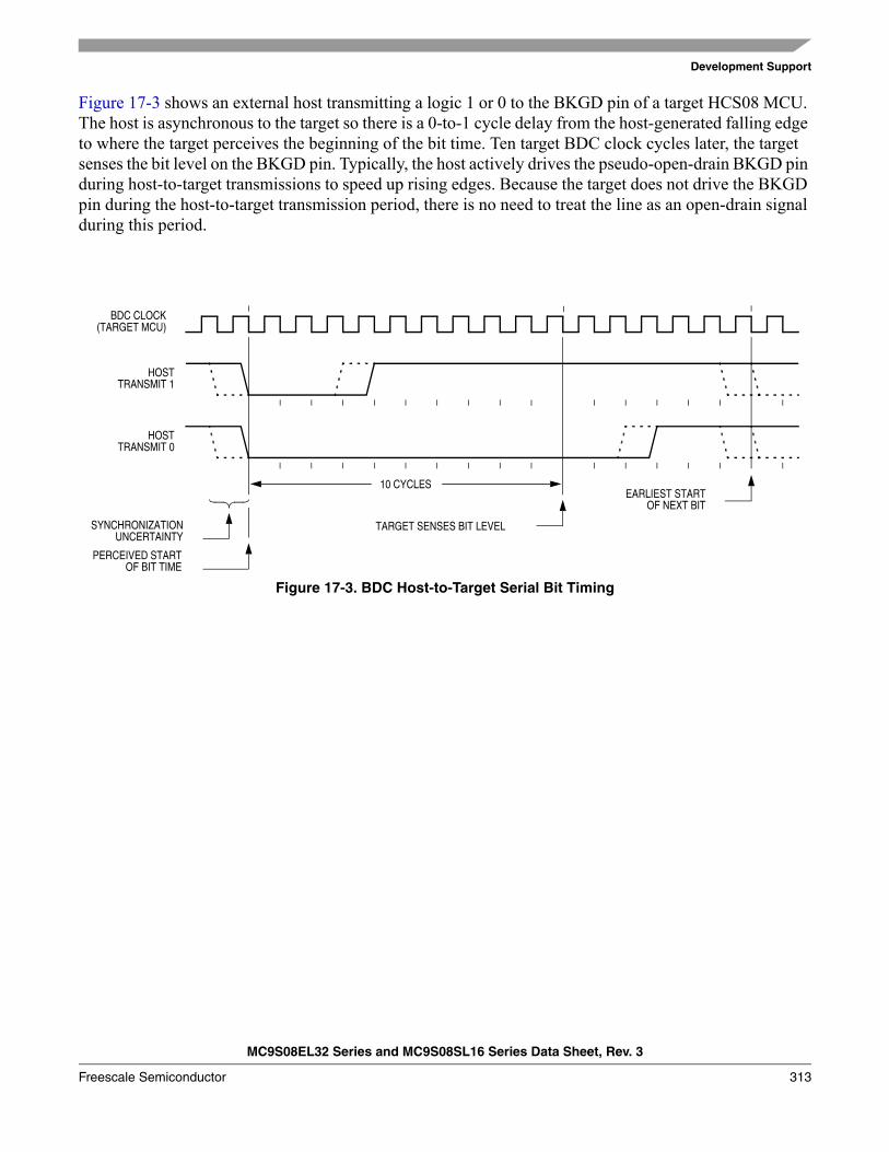
Development Support
MC9S08EL32 Series and MC9S08SL16 Series Data Sheet, Rev. 3
Freescale Semiconductor 313
Figure 17-3 shows an external host transmitting a logic 1 or 0 to the BKGD pin of a target HCS08 MCU. The host is asynchronous to the target so there is a 0-to-1 cycle delay from the host-generated falling edge to where the target perceives the beginning of the bit time. Ten target BDC clock cycles later, the target senses the bit level on the BKGD pin. Typically, the host actively drives the pseudo-open-drain BKGD pin during host-to-target transmissions to speed up rising edges. Because the target does not drive the BKGD pin during the host-to-target transmission period, there is no need to treat the line as an open-drain signal during this period.
Figure 17-3. BDC Host-to-Target Serial Bit Timing
EARLIEST START
TARGET SENSES BIT LEVEL
10 CYCLES
SYNCHRONIZATIONUNCERTAINTY
BDC CLOCK(TARGET MCU)
HOSTTRANSMIT 1
HOSTTRANSMIT 0
PERCEIVED STARTOF BIT TIME
OF NEXT BIT
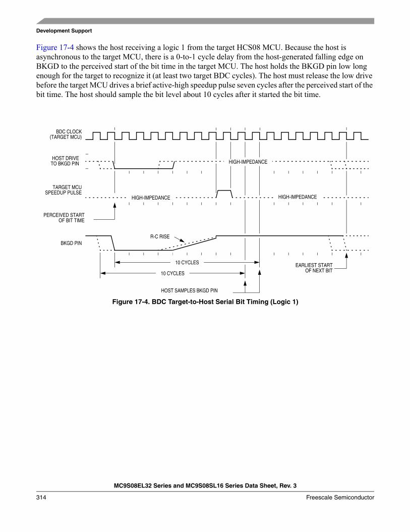
Development Support
MC9S08EL32 Series and MC9S08SL16 Series Data Sheet, Rev. 3
314 Freescale Semiconductor
Figure 17-4 shows the host receiving a logic 1 from the target HCS08 MCU. Because the host is asynchronous to the target MCU, there is a 0-to-1 cycle delay from the host-generated falling edge on BKGD to the perceived start of the bit time in the target MCU. The host holds the BKGD pin low long enough for the target to recognize it (at least two target BDC cycles). The host must release the low drive before the target MCU drives a brief active-high speedup pulse seven cycles after the perceived start of the bit time. The host should sample the bit level about 10 cycles after it started the bit time.
Figure 17-4. BDC Target-to-Host Serial Bit Timing (Logic 1)
HOST SAMPLES BKGD PIN
10 CYCLES
BDC CLOCK(TARGET MCU)
HOST DRIVETO BKGD PIN
TARGET MCUSPEEDUP PULSE
PERCEIVED STARTOF BIT TIME
HIGH-IMPEDANCE
HIGH-IMPEDANCE HIGH-IMPEDANCE
BKGD PINR-C RISE
10 CYCLES
EARLIEST STARTOF NEXT BIT
Development Support
MC9S08EL32 Series and MC9S08SL16 Series Data Sheet, Rev. 3
Freescale Semiconductor 315
Figure 17-5 shows the host receiving a logic 0 from the target HCS08 MCU. Because the host is asynchronous to the target MCU, there is a 0-to-1 cycle delay from the host-generated falling edge on BKGD to the start of the bit time as perceived by the target MCU. The host initiates the bit time but the target HCS08 finishes it. Because the target wants the host to receive a logic 0, it drives the BKGD pin low for 13 BDC clock cycles, then briefly drives it high to speed up the rising edge. The host samples the bit level about 10 cycles after starting the bit time.
Figure 17-5. BDM Target-to-Host Serial Bit Timing (Logic 0)
10 CYCLES
BDC CLOCK(TARGET MCU)
HOST DRIVETO BKGD PIN
TARGET MCUDRIVE AND
PERCEIVED STARTOF BIT TIME
HIGH-IMPEDANCE
BKGD PIN
10 CYCLES
SPEED-UP PULSE
SPEEDUPPULSE
EARLIEST STARTOF NEXT BIT
HOST SAMPLES BKGD PIN
Development Support
MC9S08EL32 Series and MC9S08SL16 Series Data Sheet, Rev. 3
316 Freescale Semiconductor
17.2.3 BDC Commands
BDC commands are sent serially from a host computer to the BKGD pin of the target HCS08 MCU. All commands and data are sent MSB-first using a custom BDC communications protocol. Active background mode commands require that the target MCU is currently in the active background mode while non-intrusive commands may be issued at any time whether the target MCU is in active background mode or running a user application program.
Table 17-1 shows all HCS08 BDC commands, a shorthand description of their coding structure, and the meaning of each command.
Coding Structure Nomenclature
This nomenclature is used in Table 17-1 to describe the coding structure of the BDC commands.Commands begin with an 8-bit hexadecimal command code in the host-to-target direction (most significant bit first)
/ = separates parts of the commandd = delay 16 target BDC clock cycles
AAAA = a 16-bit address in the host-to-target directionRD = 8 bits of read data in the target-to-host direction
WD = 8 bits of write data in the host-to-target directionRD16 = 16 bits of read data in the target-to-host direction
WD16 = 16 bits of write data in the host-to-target directionSS = the contents of BDCSCR in the target-to-host direction (STATUS)CC = 8 bits of write data for BDCSCR in the host-to-target direction (CONTROL)
RBKP = 16 bits of read data in the target-to-host direction (from BDCBKPT breakpoint register)
WBKP = 16 bits of write data in the host-to-target direction (for BDCBKPT breakpoint register)
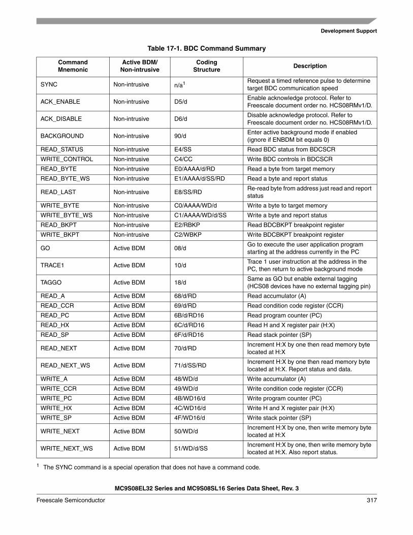
Development Support
MC9S08EL32 Series and MC9S08SL16 Series Data Sheet, Rev. 3
Freescale Semiconductor 317
Table 17-1. BDC Command Summary
CommandMnemonic
Active BDM/Non-intrusive
CodingStructure
Description
SYNC Non-intrusive n/a1
1 The SYNC command is a special operation that does not have a command code.
Request a timed reference pulse to determine target BDC communication speed
ACK_ENABLE Non-intrusive D5/dEnable acknowledge protocol. Refer to Freescale document order no. HCS08RMv1/D.
ACK_DISABLE Non-intrusive D6/dDisable acknowledge protocol. Refer to Freescale document order no. HCS08RMv1/D.
BACKGROUND Non-intrusive 90/dEnter active background mode if enabled (ignore if ENBDM bit equals 0)
READ_STATUS Non-intrusive E4/SS Read BDC status from BDCSCR
WRITE_CONTROL Non-intrusive C4/CC Write BDC controls in BDCSCR
READ_BYTE Non-intrusive E0/AAAA/d/RD Read a byte from target memory
READ_BYTE_WS Non-intrusive E1/AAAA/d/SS/RD Read a byte and report status
READ_LAST Non-intrusive E8/SS/RDRe-read byte from address just read and report status
WRITE_BYTE Non-intrusive C0/AAAA/WD/d Write a byte to target memory
WRITE_BYTE_WS Non-intrusive C1/AAAA/WD/d/SS Write a byte and report status
READ_BKPT Non-intrusive E2/RBKP Read BDCBKPT breakpoint register
WRITE_BKPT Non-intrusive C2/WBKP Write BDCBKPT breakpoint register
GO Active BDM 08/dGo to execute the user application program starting at the address currently in the PC
TRACE1 Active BDM 10/dTrace 1 user instruction at the address in the PC, then return to active background mode
TAGGO Active BDM 18/dSame as GO but enable external tagging (HCS08 devices have no external tagging pin)
READ_A Active BDM 68/d/RD Read accumulator (A)
READ_CCR Active BDM 69/d/RD Read condition code register (CCR)
READ_PC Active BDM 6B/d/RD16 Read program counter (PC)
READ_HX Active BDM 6C/d/RD16 Read H and X register pair (H:X)
READ_SP Active BDM 6F/d/RD16 Read stack pointer (SP)
READ_NEXT Active BDM 70/d/RDIncrement H:X by one then read memory byte located at H:X
READ_NEXT_WS Active BDM 71/d/SS/RDIncrement H:X by one then read memory byte located at H:X. Report status and data.
WRITE_A Active BDM 48/WD/d Write accumulator (A)
WRITE_CCR Active BDM 49/WD/d Write condition code register (CCR)
WRITE_PC Active BDM 4B/WD16/d Write program counter (PC)
WRITE_HX Active BDM 4C/WD16/d Write H and X register pair (H:X)
WRITE_SP Active BDM 4F/WD16/d Write stack pointer (SP)
WRITE_NEXT Active BDM 50/WD/dIncrement H:X by one, then write memory byte located at H:X
WRITE_NEXT_WS Active BDM 51/WD/d/SSIncrement H:X by one, then write memory byte located at H:X. Also report status.
Development Support
MC9S08EL32 Series and MC9S08SL16 Series Data Sheet, Rev. 3
318 Freescale Semiconductor
The SYNC command is unlike other BDC commands because the host does not necessarily know the correct communications speed to use for BDC communications until after it has analyzed the response to the SYNC command.
To issue a SYNC command, the host:• Drives the BKGD pin low for at least 128 cycles of the slowest possible BDC clock (The slowest
clock is normally the reference oscillator/64 or the self-clocked rate/64.)• Drives BKGD high for a brief speedup pulse to get a fast rise time (This speedup pulse is typically
one cycle of the fastest clock in the system.)• Removes all drive to the BKGD pin so it reverts to high impedance• Monitors the BKGD pin for the sync response pulse
The target, upon detecting the SYNC request from the host (which is a much longer low time than would ever occur during normal BDC communications):
• Waits for BKGD to return to a logic high• Delays 16 cycles to allow the host to stop driving the high speedup pulse• Drives BKGD low for 128 BDC clock cycles• Drives a 1-cycle high speedup pulse to force a fast rise time on BKGD• Removes all drive to the BKGD pin so it reverts to high impedance
The host measures the low time of this 128-cycle sync response pulse and determines the correct speed for subsequent BDC communications. Typically, the host can determine the correct communication speed within a few percent of the actual target speed and the communication protocol can easily tolerate speed errors of several percent.
17.2.4 BDC Hardware Breakpoint
The BDC includes one relatively simple hardware breakpoint that compares the CPU address bus to a 16-bit match value in the BDCBKPT register. This breakpoint can generate a forced breakpoint or a tagged breakpoint. A forced breakpoint causes the CPU to enter active background mode at the first instruction boundary following any access to the breakpoint address. The tagged breakpoint causes the instruction opcode at the breakpoint address to be tagged so that the CPU will enter active background mode rather than executing that instruction if and when it reaches the end of the instruction queue. This implies that tagged breakpoints can only be placed at the address of an instruction opcode while forced breakpoints can be set at any address.
The breakpoint enable (BKPTEN) control bit in the BDC status and control register (BDCSCR) is used to enable the breakpoint logic (BKPTEN = 1). When BKPTEN = 0, its default value after reset, the breakpoint logic is disabled and no BDC breakpoints are requested regardless of the values in other BDC breakpoint registers and control bits. The force/tag select (FTS) control bit in BDCSCR is used to select forced (FTS = 1) or tagged (FTS = 0) type breakpoints.
The on-chip debug module (DBG) includes circuitry for two additional hardware breakpoints that are more flexible than the simple breakpoint in the BDC module.
Development Support
MC9S08EL32 Series and MC9S08SL16 Series Data Sheet, Rev. 3
Freescale Semiconductor 319
17.3 On-Chip Debug System (DBG)Because HCS08 devices do not have external address and data buses, the most important functions of an in-circuit emulator have been built onto the chip with the MCU. The debug system consists of an 8-stage FIFO that can store address or data bus information, and a flexible trigger system to decide when to capture bus information and what information to capture. The system relies on the single-wire background debug system to access debug control registers and to read results out of the eight stage FIFO.
The debug module includes control and status registers that are accessible in the user’s memory map. These registers are located in the high register space to avoid using valuable direct page memory space.
Most of the debug module’s functions are used during development, and user programs rarely access any of the control and status registers for the debug module. The one exception is that the debug system can provide the means to implement a form of ROM patching. This topic is discussed in greater detail in Section 17.3.6, “Hardware Breakpoints.”
17.3.1 Comparators A and B
Two 16-bit comparators (A and B) can optionally be qualified with the R/W signal and an opcode tracking circuit. Separate control bits allow you to ignore R/W for each comparator. The opcode tracking circuitry optionally allows you to specify that a trigger will occur only if the opcode at the specified address is actually executed as opposed to only being read from memory into the instruction queue. The comparators are also capable of magnitude comparisons to support the inside range and outside range trigger modes. Comparators are disabled temporarily during all BDC accesses.
The A comparator is always associated with the 16-bit CPU address. The B comparator compares to the CPU address or the 8-bit CPU data bus, depending on the trigger mode selected. Because the CPU data bus is separated into a read data bus and a write data bus, the RWAEN and RWA control bits have an additional purpose, in full address plus data comparisons they are used to decide which of these buses to use in the comparator B data bus comparisons. If RWAEN = 1 (enabled) and RWA = 0 (write), the CPU’s write data bus is used. Otherwise, the CPU’s read data bus is used.
The currently selected trigger mode determines what the debugger logic does when a comparator detects a qualified match condition. A match can cause:
• Generation of a breakpoint to the CPU • Storage of data bus values into the FIFO• Starting to store change-of-flow addresses into the FIFO (begin type trace)• Stopping the storage of change-of-flow addresses into the FIFO (end type trace)
17.3.2 Bus Capture Information and FIFO Operation
The usual way to use the FIFO is to setup the trigger mode and other control options, then arm the debugger. When the FIFO has filled or the debugger has stopped storing data into the FIFO, you would read the information out of it in the order it was stored into the FIFO. Status bits indicate the number of words of valid information that are in the FIFO as data is stored into it. If a trace run is manually halted by writing 0 to ARM before the FIFO is full (CNT = 1:0:0:0), the information is shifted by one position and
Development Support
MC9S08EL32 Series and MC9S08SL16 Series Data Sheet, Rev. 3
320 Freescale Semiconductor
the host must perform ((8 – CNT) – 1) dummy reads of the FIFO to advance it to the first significant entry in the FIFO.
In most trigger modes, the information stored in the FIFO consists of 16-bit change-of-flow addresses. In these cases, read DBGFH then DBGFL to get one coherent word of information out of the FIFO. Reading DBGFL (the low-order byte of the FIFO data port) causes the FIFO to shift so the next word of information is available at the FIFO data port. In the event-only trigger modes (see Section 17.3.5, “Trigger Modes”), 8-bit data information is stored into the FIFO. In these cases, the high-order half of the FIFO (DBGFH) is not used and data is read out of the FIFO by simply reading DBGFL. Each time DBGFL is read, the FIFO is shifted so the next data value is available through the FIFO data port at DBGFL.
In trigger modes where the FIFO is storing change-of-flow addresses, there is a delay between CPU addresses and the input side of the FIFO. Because of this delay, if the trigger event itself is a change-of-flow address or a change-of-flow address appears during the next two bus cycles after a trigger event starts the FIFO, it will not be saved into the FIFO. In the case of an end-trace, if the trigger event is a change-of-flow, it will be saved as the last change-of-flow entry for that debug run.
The FIFO can also be used to generate a profile of executed instruction addresses when the debugger is not armed. When ARM = 0, reading DBGFL causes the address of the most-recently fetched opcode to be saved in the FIFO. To use the profiling feature, a host debugger would read addresses out of the FIFO by reading DBGFH then DBGFL at regular periodic intervals. The first eight values would be discarded because they correspond to the eight DBGFL reads needed to initially fill the FIFO. Additional periodic reads of DBGFH and DBGFL return delayed information about executed instructions so the host debugger can develop a profile of executed instruction addresses.
17.3.3 Change-of-Flow Information
To minimize the amount of information stored in the FIFO, only information related to instructions that cause a change to the normal sequential execution of instructions is stored. With knowledge of the source and object code program stored in the target system, an external debugger system can reconstruct the path of execution through many instructions from the change-of-flow information stored in the FIFO.
For conditional branch instructions where the branch is taken (branch condition was true), the source address is stored (the address of the conditional branch opcode). Because BRA and BRN instructions are not conditional, these events do not cause change-of-flow information to be stored in the FIFO.
Indirect JMP and JSR instructions use the current contents of the H:X index register pair to determine the destination address, so the debug system stores the run-time destination address for any indirect JMP or JSR. For interrupts, RTI, or RTS, the destination address is stored in the FIFO as change-of-flow information.
17.3.4 Tag vs. Force Breakpoints and Triggers
Tagging is a term that refers to identifying an instruction opcode as it is fetched into the instruction queue, but not taking any other action until and unless that instruction is actually executed by the CPU. This distinction is important because any change-of-flow from a jump, branch, subroutine call, or interrupt causes some instructions that have been fetched into the instruction queue to be thrown away without being executed.
Development Support
MC9S08EL32 Series and MC9S08SL16 Series Data Sheet, Rev. 3
Freescale Semiconductor 321
A force-type breakpoint waits for the current instruction to finish and then acts upon the breakpoint request. The usual action in response to a breakpoint is to go to active background mode rather than continuing to the next instruction in the user application program.
The tag vs. force terminology is used in two contexts within the debug module. The first context refers to breakpoint requests from the debug module to the CPU. The second refers to match signals from the comparators to the debugger control logic. When a tag-type break request is sent to the CPU, a signal is entered into the instruction queue along with the opcode so that if/when this opcode ever executes, the CPU will effectively replace the tagged opcode with a BGND opcode so the CPU goes to active background mode rather than executing the tagged instruction. When the TRGSEL control bit in the DBGT register is set to select tag-type operation, the output from comparator A or B is qualified by a block of logic in the debug module that tracks opcodes and only produces a trigger to the debugger if the opcode at the compare address is actually executed. There is separate opcode tracking logic for each comparator so more than one compare event can be tracked through the instruction queue at a time.
17.3.5 Trigger Modes
The trigger mode controls the overall behavior of a debug run. The 4-bit TRG field in the DBGT register selects one of nine trigger modes. When TRGSEL = 1 in the DBGT register, the output of the comparator must propagate through an opcode tracking circuit before triggering FIFO actions. The BEGIN bit in DBGT chooses whether the FIFO begins storing data when the qualified trigger is detected (begin trace), or the FIFO stores data in a circular fashion from the time it is armed until the qualified trigger is detected (end trigger).
A debug run is started by writing a 1 to the ARM bit in the DBGC register, which sets the ARMF flag and clears the AF and BF flags and the CNT bits in DBGS. A begin-trace debug run ends when the FIFO gets full. An end-trace run ends when the selected trigger event occurs. Any debug run can be stopped manually by writing a 0 to ARM or DBGEN in DBGC.
In all trigger modes except event-only modes, the FIFO stores change-of-flow addresses. In event-only trigger modes, the FIFO stores data in the low-order eight bits of the FIFO.
The BEGIN control bit is ignored in event-only trigger modes and all such debug runs are begin type traces. When TRGSEL = 1 to select opcode fetch triggers, it is not necessary to use R/W in comparisons because opcode tags would only apply to opcode fetches that are always read cycles. It would also be unusual to specify TRGSEL = 1 while using a full mode trigger because the opcode value is normally known at a particular address.
The following trigger mode descriptions only state the primary comparator conditions that lead to a trigger. Either comparator can usually be further qualified with R/W by setting RWAEN (RWBEN) and the corresponding RWA (RWB) value to be matched against R/W. The signal from the comparator with optional R/W qualification is used to request a CPU breakpoint if BRKEN = 1 and TAG determines whether the CPU request will be a tag request or a force request.
Development Support
MC9S08EL32 Series and MC9S08SL16 Series Data Sheet, Rev. 3
322 Freescale Semiconductor
A-Only — Trigger when the address matches the value in comparator A
A OR B — Trigger when the address matches either the value in comparator A or the value in comparator B
A Then B — Trigger when the address matches the value in comparator B but only after the address for another cycle matched the value in comparator A. There can be any number of cycles after the A match and before the B match.
A AND B Data (Full Mode) — This is called a full mode because address, data, and R/W (optionally) must match within the same bus cycle to cause a trigger event. Comparator A checks address, the low byte of comparator B checks data, and R/W is checked against RWA if RWAEN = 1. The high-order half of comparator B is not used.
In full trigger modes it is not useful to specify a tag-type CPU breakpoint (BRKEN = TAG = 1), but if you do, the comparator B data match is ignored for the purpose of issuing the tag request to the CPU and the CPU breakpoint is issued when the comparator A address matches.
A AND NOT B Data (Full Mode) — Address must match comparator A, data must not match the low half of comparator B, and R/W must match RWA if RWAEN = 1. All three conditions must be met within the same bus cycle to cause a trigger.
In full trigger modes it is not useful to specify a tag-type CPU breakpoint (BRKEN = TAG = 1), but if you do, the comparator B data match is ignored for the purpose of issuing the tag request to the CPU and the CPU breakpoint is issued when the comparator A address matches.
Event-Only B (Store Data) — Trigger events occur each time the address matches the value in comparator B. Trigger events cause the data to be captured into the FIFO. The debug run ends when the FIFO becomes full.
A Then Event-Only B (Store Data) — After the address has matched the value in comparator A, a trigger event occurs each time the address matches the value in comparator B. Trigger events cause the data to be captured into the FIFO. The debug run ends when the FIFO becomes full.
Inside Range (A ≤ Address ≤ B) — A trigger occurs when the address is greater than or equal to the value in comparator A and less than or equal to the value in comparator B at the same time.
Outside Range (Address < A or Address > B) — A trigger occurs when the address is either less than the value in comparator A or greater than the value in comparator B.
Development Support
MC9S08EL32 Series and MC9S08SL16 Series Data Sheet, Rev. 3
Freescale Semiconductor 323
17.3.6 Hardware Breakpoints
The BRKEN control bit in the DBGC register may be set to 1 to allow any of the trigger conditions described in Section 17.3.5, “Trigger Modes,” to be used to generate a hardware breakpoint request to the CPU. TAG in DBGC controls whether the breakpoint request will be treated as a tag-type breakpoint or a force-type breakpoint. A tag breakpoint causes the current opcode to be marked as it enters the instruction queue. If a tagged opcode reaches the end of the pipe, the CPU executes a BGND instruction to go to active background mode rather than executing the tagged opcode. A force-type breakpoint causes the CPU to finish the current instruction and then go to active background mode.
If the background mode has not been enabled (ENBDM = 1) by a serial WRITE_CONTROL command through the BKGD pin, the CPU will execute an SWI instruction instead of going to active background mode.
17.4 Register Definition
This section contains the descriptions of the BDC and DBG registers and control bits.
Refer to the high-page register summary in the device overview chapter of this data sheet for the absolute address assignments for all DBG registers. This section refers to registers and control bits only by their names. A Freescale-provided equate or header file is used to translate these names into the appropriate absolute addresses.
17.4.1 BDC Registers and Control Bits
The BDC has two registers:• The BDC status and control register (BDCSCR) is an 8-bit register containing control and status
bits for the background debug controller. • The BDC breakpoint match register (BDCBKPT) holds a 16-bit breakpoint match address.
These registers are accessed with dedicated serial BDC commands and are not located in the memory space of the target MCU (so they do not have addresses and cannot be accessed by user programs).
Some of the bits in the BDCSCR have write limitations; otherwise, these registers may be read or written at any time. For example, the ENBDM control bit may not be written while the MCU is in active background mode. (This prevents the ambiguous condition of the control bit forbidding active background mode while the MCU is already in active background mode.) Also, the four status bits (BDMACT, WS, WSF, and DVF) are read-only status indicators and can never be written by the WRITE_CONTROL serial BDC command. The clock switch (CLKSW) control bit may be read or written at any time.
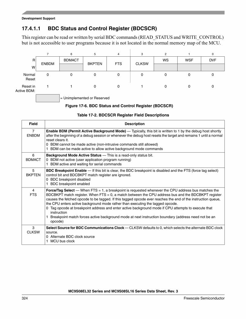
Development Support
MC9S08EL32 Series and MC9S08SL16 Series Data Sheet, Rev. 3
324 Freescale Semiconductor
17.4.1.1 BDC Status and Control Register (BDCSCR)
This register can be read or written by serial BDC commands (READ_STATUS and WRITE_CONTROL) but is not accessible to user programs because it is not located in the normal memory map of the MCU.
7 6 5 4 3 2 1 0
RENBDM
BDMACTBKPTEN FTS CLKSW
WS WSF DVF
W
NormalReset
0 0 0 0 0 0 0 0
Reset inActive BDM:
1 1 0 0 1 0 0 0
= Unimplemented or Reserved
Figure 17-6. BDC Status and Control Register (BDCSCR)
Table 17-2. BDCSCR Register Field Descriptions
Field Description
7ENBDM
Enable BDM (Permit Active Background Mode) — Typically, this bit is written to 1 by the debug host shortly after the beginning of a debug session or whenever the debug host resets the target and remains 1 until a normal reset clears it.0 BDM cannot be made active (non-intrusive commands still allowed)1 BDM can be made active to allow active background mode commands
6BDMACT
Background Mode Active Status — This is a read-only status bit.0 BDM not active (user application program running)1 BDM active and waiting for serial commands
5BKPTEN
BDC Breakpoint Enable — If this bit is clear, the BDC breakpoint is disabled and the FTS (force tag select) control bit and BDCBKPT match register are ignored.0 BDC breakpoint disabled1 BDC breakpoint enabled
4FTS
Force/Tag Select — When FTS = 1, a breakpoint is requested whenever the CPU address bus matches the BDCBKPT match register. When FTS = 0, a match between the CPU address bus and the BDCBKPT register causes the fetched opcode to be tagged. If this tagged opcode ever reaches the end of the instruction queue, the CPU enters active background mode rather than executing the tagged opcode.0 Tag opcode at breakpoint address and enter active background mode if CPU attempts to execute that
instruction1 Breakpoint match forces active background mode at next instruction boundary (address need not be an
opcode)
3CLKSW
Select Source for BDC Communications Clock — CLKSW defaults to 0, which selects the alternate BDC clock source.0 Alternate BDC clock source1 MCU bus clock
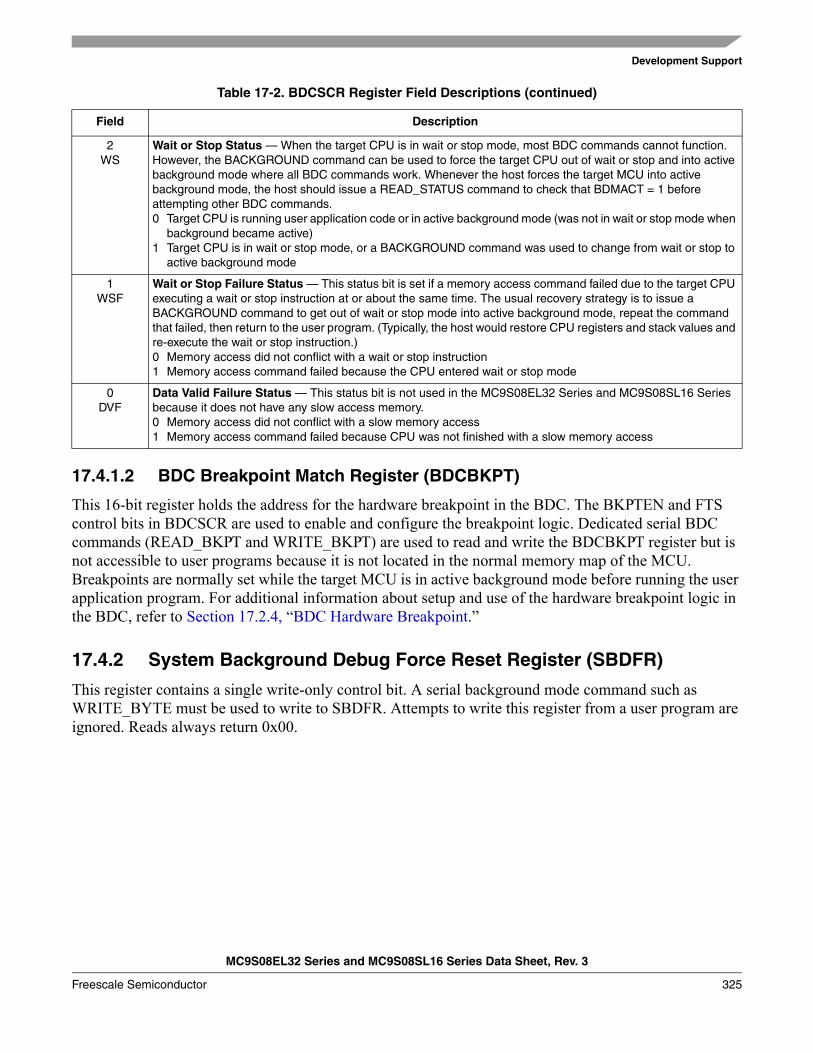
Development Support
MC9S08EL32 Series and MC9S08SL16 Series Data Sheet, Rev. 3
Freescale Semiconductor 325
17.4.1.2 BDC Breakpoint Match Register (BDCBKPT)
This 16-bit register holds the address for the hardware breakpoint in the BDC. The BKPTEN and FTS control bits in BDCSCR are used to enable and configure the breakpoint logic. Dedicated serial BDC commands (READ_BKPT and WRITE_BKPT) are used to read and write the BDCBKPT register but is not accessible to user programs because it is not located in the normal memory map of the MCU. Breakpoints are normally set while the target MCU is in active background mode before running the user application program. For additional information about setup and use of the hardware breakpoint logic in the BDC, refer to Section 17.2.4, “BDC Hardware Breakpoint.”
17.4.2 System Background Debug Force Reset Register (SBDFR)
This register contains a single write-only control bit. A serial background mode command such as WRITE_BYTE must be used to write to SBDFR. Attempts to write this register from a user program are ignored. Reads always return 0x00.
2WS
Wait or Stop Status — When the target CPU is in wait or stop mode, most BDC commands cannot function. However, the BACKGROUND command can be used to force the target CPU out of wait or stop and into active background mode where all BDC commands work. Whenever the host forces the target MCU into active background mode, the host should issue a READ_STATUS command to check that BDMACT = 1 before attempting other BDC commands.0 Target CPU is running user application code or in active background mode (was not in wait or stop mode when
background became active)1 Target CPU is in wait or stop mode, or a BACKGROUND command was used to change from wait or stop to
active background mode
1WSF
Wait or Stop Failure Status — This status bit is set if a memory access command failed due to the target CPU executing a wait or stop instruction at or about the same time. The usual recovery strategy is to issue a BACKGROUND command to get out of wait or stop mode into active background mode, repeat the command that failed, then return to the user program. (Typically, the host would restore CPU registers and stack values and re-execute the wait or stop instruction.)0 Memory access did not conflict with a wait or stop instruction1 Memory access command failed because the CPU entered wait or stop mode
0DVF
Data Valid Failure Status — This status bit is not used in the MC9S08EL32 Series and MC9S08SL16 Series because it does not have any slow access memory.0 Memory access did not conflict with a slow memory access1 Memory access command failed because CPU was not finished with a slow memory access
Table 17-2. BDCSCR Register Field Descriptions (continued)
Field Description
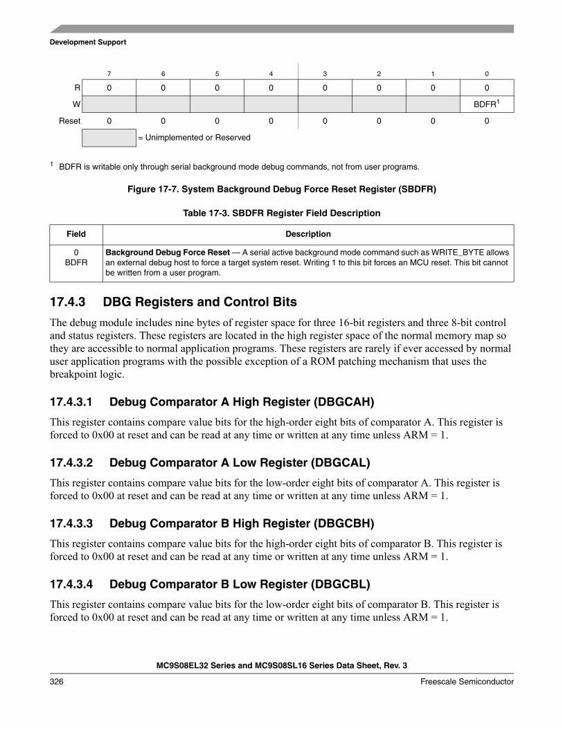
Development Support
MC9S08EL32 Series and MC9S08SL16 Series Data Sheet, Rev. 3
326 Freescale Semiconductor
Figure 17-7. System Background Debug Force Reset Register (SBDFR)
17.4.3 DBG Registers and Control Bits
The debug module includes nine bytes of register space for three 16-bit registers and three 8-bit control and status registers. These registers are located in the high register space of the normal memory map so they are accessible to normal application programs. These registers are rarely if ever accessed by normal user application programs with the possible exception of a ROM patching mechanism that uses the breakpoint logic.
17.4.3.1 Debug Comparator A High Register (DBGCAH)
This register contains compare value bits for the high-order eight bits of comparator A. This register is forced to 0x00 at reset and can be read at any time or written at any time unless ARM = 1.
17.4.3.2 Debug Comparator A Low Register (DBGCAL)
This register contains compare value bits for the low-order eight bits of comparator A. This register is forced to 0x00 at reset and can be read at any time or written at any time unless ARM = 1.
17.4.3.3 Debug Comparator B High Register (DBGCBH)
This register contains compare value bits for the high-order eight bits of comparator B. This register is forced to 0x00 at reset and can be read at any time or written at any time unless ARM = 1.
17.4.3.4 Debug Comparator B Low Register (DBGCBL)
This register contains compare value bits for the low-order eight bits of comparator B. This register is forced to 0x00 at reset and can be read at any time or written at any time unless ARM = 1.
7 6 5 4 3 2 1 0
R 0 0 0 0 0 0 0 0
W BDFR1
1 BDFR is writable only through serial background mode debug commands, not from user programs.
Reset 0 0 0 0 0 0 0 0
= Unimplemented or Reserved
Table 17-3. SBDFR Register Field Description
Field Description
0BDFR
Background Debug Force Reset — A serial active background mode command such as WRITE_BYTE allows an external debug host to force a target system reset. Writing 1 to this bit forces an MCU reset. This bit cannot be written from a user program.
Development Support
MC9S08EL32 Series and MC9S08SL16 Series Data Sheet, Rev. 3
Freescale Semiconductor 327
17.4.3.5 Debug FIFO High Register (DBGFH)
This register provides read-only access to the high-order eight bits of the FIFO. Writes to this register have no meaning or effect. In the event-only trigger modes, the FIFO only stores data into the low-order byte of each FIFO word, so this register is not used and will read 0x00.
Reading DBGFH does not cause the FIFO to shift to the next word. When reading 16-bit words out of the FIFO, read DBGFH before reading DBGFL because reading DBGFL causes the FIFO to advance to the next word of information.
17.4.3.6 Debug FIFO Low Register (DBGFL)
This register provides read-only access to the low-order eight bits of the FIFO. Writes to this register have no meaning or effect.
Reading DBGFL causes the FIFO to shift to the next available word of information. When the debug module is operating in event-only modes, only 8-bit data is stored into the FIFO (high-order half of each FIFO word is unused). When reading 8-bit words out of the FIFO, simply read DBGFL repeatedly to get successive bytes of data from the FIFO. It isn’t necessary to read DBGFH in this case.
Do not attempt to read data from the FIFO while it is still armed (after arming but before the FIFO is filled or ARMF is cleared) because the FIFO is prevented from advancing during reads of DBGFL. This can interfere with normal sequencing of reads from the FIFO.
Reading DBGFL while the debugger is not armed causes the address of the most-recently fetched opcode to be stored to the last location in the FIFO. By reading DBGFH then DBGFL periodically, external host software can develop a profile of program execution. After eight reads from the FIFO, the ninth read will return the information that was stored as a result of the first read. To use the profiling feature, read the FIFO eight times without using the data to prime the sequence and then begin using the data to get a delayed picture of what addresses were being executed. The information stored into the FIFO on reads of DBGFL (while the FIFO is not armed) is the address of the most-recently fetched opcode.
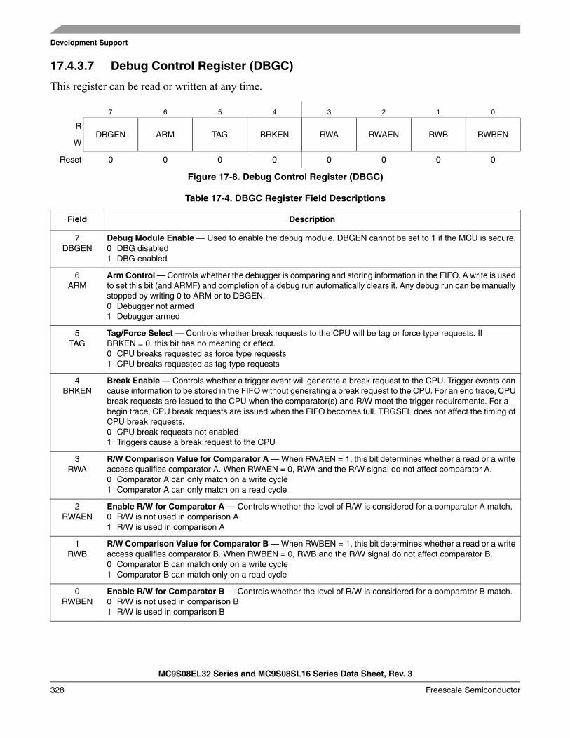
Development Support
MC9S08EL32 Series and MC9S08SL16 Series Data Sheet, Rev. 3
328 Freescale Semiconductor
17.4.3.7 Debug Control Register (DBGC)
This register can be read or written at any time.
7 6 5 4 3 2 1 0
RDBGEN ARM TAG BRKEN RWA RWAEN RWB RWBEN
W
Reset 0 0 0 0 0 0 0 0
Figure 17-8. Debug Control Register (DBGC)
Table 17-4. DBGC Register Field Descriptions
Field Description
7DBGEN
Debug Module Enable — Used to enable the debug module. DBGEN cannot be set to 1 if the MCU is secure.0 DBG disabled1 DBG enabled
6ARM
Arm Control — Controls whether the debugger is comparing and storing information in the FIFO. A write is used to set this bit (and ARMF) and completion of a debug run automatically clears it. Any debug run can be manually stopped by writing 0 to ARM or to DBGEN.0 Debugger not armed1 Debugger armed
5TAG
Tag/Force Select — Controls whether break requests to the CPU will be tag or force type requests. If BRKEN = 0, this bit has no meaning or effect.0 CPU breaks requested as force type requests1 CPU breaks requested as tag type requests
4BRKEN
Break Enable — Controls whether a trigger event will generate a break request to the CPU. Trigger events can cause information to be stored in the FIFO without generating a break request to the CPU. For an end trace, CPU break requests are issued to the CPU when the comparator(s) and R/W meet the trigger requirements. For a begin trace, CPU break requests are issued when the FIFO becomes full. TRGSEL does not affect the timing of CPU break requests.0 CPU break requests not enabled1 Triggers cause a break request to the CPU
3RWA
R/W Comparison Value for Comparator A — When RWAEN = 1, this bit determines whether a read or a write access qualifies comparator A. When RWAEN = 0, RWA and the R/W signal do not affect comparator A.0 Comparator A can only match on a write cycle1 Comparator A can only match on a read cycle
2RWAEN
Enable R/W for Comparator A — Controls whether the level of R/W is considered for a comparator A match.0 R/W is not used in comparison A1 R/W is used in comparison A
1RWB
R/W Comparison Value for Comparator B — When RWBEN = 1, this bit determines whether a read or a write access qualifies comparator B. When RWBEN = 0, RWB and the R/W signal do not affect comparator B.0 Comparator B can match only on a write cycle1 Comparator B can match only on a read cycle
0RWBEN
Enable R/W for Comparator B — Controls whether the level of R/W is considered for a comparator B match.0 R/W is not used in comparison B1 R/W is used in comparison B
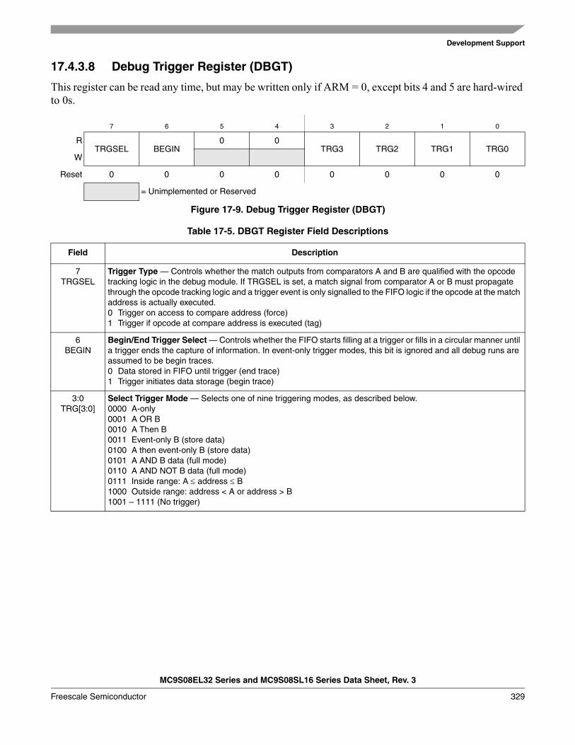
Development Support
MC9S08EL32 Series and MC9S08SL16 Series Data Sheet, Rev. 3
Freescale Semiconductor 329
17.4.3.8 Debug Trigger Register (DBGT)
This register can be read any time, but may be written only if ARM = 0, except bits 4 and 5 are hard-wired to 0s.
7 6 5 4 3 2 1 0
RTRGSEL BEGIN
0 0TRG3 TRG2 TRG1 TRG0
W
Reset 0 0 0 0 0 0 0 0
= Unimplemented or Reserved
Figure 17-9. Debug Trigger Register (DBGT)
Table 17-5. DBGT Register Field Descriptions
Field Description
7TRGSEL
Trigger Type — Controls whether the match outputs from comparators A and B are qualified with the opcode tracking logic in the debug module. If TRGSEL is set, a match signal from comparator A or B must propagate through the opcode tracking logic and a trigger event is only signalled to the FIFO logic if the opcode at the match address is actually executed.0 Trigger on access to compare address (force)1 Trigger if opcode at compare address is executed (tag)
6BEGIN
Begin/End Trigger Select — Controls whether the FIFO starts filling at a trigger or fills in a circular manner until a trigger ends the capture of information. In event-only trigger modes, this bit is ignored and all debug runs are assumed to be begin traces.0 Data stored in FIFO until trigger (end trace)1 Trigger initiates data storage (begin trace)
3:0TRG[3:0]
Select Trigger Mode — Selects one of nine triggering modes, as described below.0000 A-only0001 A OR B0010 A Then B0011 Event-only B (store data)0100 A then event-only B (store data)0101 A AND B data (full mode)0110 A AND NOT B data (full mode)0111 Inside range: A ≤ address ≤ B1000 Outside range: address < A or address > B1001 – 1111 (No trigger)
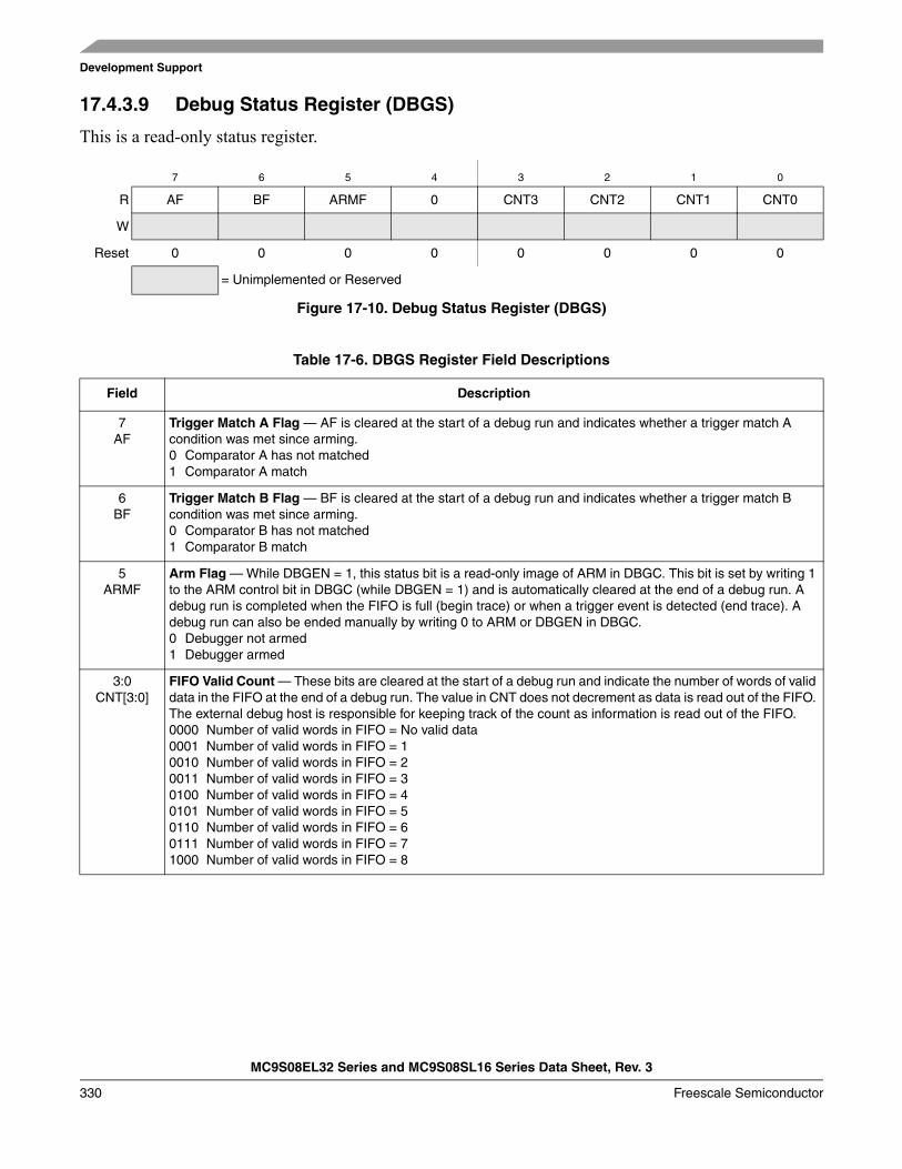
Development Support
MC9S08EL32 Series and MC9S08SL16 Series Data Sheet, Rev. 3
330 Freescale Semiconductor
17.4.3.9 Debug Status Register (DBGS)
This is a read-only status register.
7 6 5 4 3 2 1 0
R AF BF ARMF 0 CNT3 CNT2 CNT1 CNT0
W
Reset 0 0 0 0 0 0 0 0
= Unimplemented or Reserved
Figure 17-10. Debug Status Register (DBGS)
Table 17-6. DBGS Register Field Descriptions
Field Description
7AF
Trigger Match A Flag — AF is cleared at the start of a debug run and indicates whether a trigger match A condition was met since arming.0 Comparator A has not matched1 Comparator A match
6BF
Trigger Match B Flag — BF is cleared at the start of a debug run and indicates whether a trigger match B condition was met since arming.0 Comparator B has not matched1 Comparator B match
5ARMF
Arm Flag — While DBGEN = 1, this status bit is a read-only image of ARM in DBGC. This bit is set by writing 1 to the ARM control bit in DBGC (while DBGEN = 1) and is automatically cleared at the end of a debug run. A debug run is completed when the FIFO is full (begin trace) or when a trigger event is detected (end trace). A debug run can also be ended manually by writing 0 to ARM or DBGEN in DBGC.0 Debugger not armed1 Debugger armed
3:0CNT[3:0]
FIFO Valid Count — These bits are cleared at the start of a debug run and indicate the number of words of valid data in the FIFO at the end of a debug run. The value in CNT does not decrement as data is read out of the FIFO. The external debug host is responsible for keeping track of the count as information is read out of the FIFO. 0000 Number of valid words in FIFO = No valid data0001 Number of valid words in FIFO = 10010 Number of valid words in FIFO = 20011 Number of valid words in FIFO = 30100 Number of valid words in FIFO = 40101 Number of valid words in FIFO = 50110 Number of valid words in FIFO = 60111 Number of valid words in FIFO = 71000 Number of valid words in FIFO = 8
MC9S08EL32 Series and MC9S08SL16 Series Data Sheet, Rev. 3
Freescale Semiconductor 331
Appendix AElectrical Characteristics
A.1 IntroductionThis section contains the most accurate electrical and timing information for the MC9S08EL32 Series and MC9S08SL16 Series of microcontrollers available at the time of publication.
A.2 Parameter ClassificationThe electrical parameters shown in this supplement are guaranteed by various methods. To give the customer a better understanding the following classification is used and the parameters are tagged accordingly in the tables where appropriate:
NOTEThe classification is shown in the column labeled “C” in the parameter tables where appropriate.
A.3 Absolute Maximum RatingsAbsolute maximum ratings are stress ratings only, and functional operation at the maxima is not guaranteed. Stress beyond the limits specified in Table A-2 may affect device reliability or cause permanent damage to the device. For functional operating conditions, refer to the remaining tables in this section.
This device contains circuitry protecting against damage due to high static voltage or electrical fields; however, it is advised that normal precautions be taken to avoid application of any voltages higher than maximum-rated voltages to this high-impedance circuit. Reliability of operation is enhanced if unused inputs are tied to an appropriate logic voltage level (for instance, either VSS or VDD) or the programmable pull-up resistor associated with the pin is enabled.
Table A-1. Parameter Classifications
P Those parameters are guaranteed during production testing on each individual device.
C Those parameters are achieved by the design characterization by measuring a statistically relevant sample size across process variations.
TThose parameters are achieved by design characterization on a small sample size from typical devices under typical conditions unless otherwise noted. All values shown in the typical column are within this category.
D Those parameters are derived mainly from simulations.
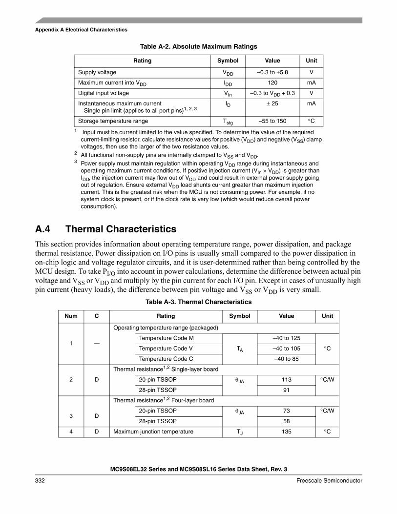
Appendix A Electrical Characteristics
MC9S08EL32 Series and MC9S08SL16 Series Data Sheet, Rev. 3
332 Freescale Semiconductor
A.4 Thermal CharacteristicsThis section provides information about operating temperature range, power dissipation, and package thermal resistance. Power dissipation on I/O pins is usually small compared to the power dissipation in on-chip logic and voltage regulator circuits, and it is user-determined rather than being controlled by the MCU design. To take PI/O into account in power calculations, determine the difference between actual pin voltage and VSS or VDD and multiply by the pin current for each I/O pin. Except in cases of unusually high pin current (heavy loads), the difference between pin voltage and VSS or VDD is very small.
Table A-2. Absolute Maximum Ratings
Rating Symbol Value Unit
Supply voltage VDD –0.3 to +5.8 V
Maximum current into VDD IDD 120 mA
Digital input voltage VIn –0.3 to VDD + 0.3 V
Instantaneous maximum current Single pin limit (applies to all port pins)1, 2, 3
1 Input must be current limited to the value specified. To determine the value of the required current-limiting resistor, calculate resistance values for positive (VDD) and negative (VSS) clamp voltages, then use the larger of the two resistance values.
2 All functional non-supply pins are internally clamped to VSS and VDD.3 Power supply must maintain regulation within operating VDD range during instantaneous and
operating maximum current conditions. If positive injection current (VIn > VDD) is greater than IDD, the injection current may flow out of VDD and could result in external power supply going out of regulation. Ensure external VDD load shunts current greater than maximum injection current. This is the greatest risk when the MCU is not consuming power. For example, if no system clock is present, or if the clock rate is very low (which would reduce overall power consumption).
ID ± 25 mA
Storage temperature range Tstg –55 to 150 °C
Table A-3. Thermal Characteristics
Num C Rating Symbol Value Unit
1 —
Operating temperature range (packaged)
Temperature Code M
TA
–40 to 125
°CTemperature Code V –40 to 105
Temperature Code C –40 to 85
2 D
Thermal resistance1,2 Single-layer board
20-pin TSSOP θJA 113 °C/W
28-pin TSSOP 91
3 D
Thermal resistance1,2 Four-layer board
20-pin TSSOP θJA 73 °C/W
28-pin TSSOP 58
4 D Maximum junction temperature TJ 135 °C
Appendix A Electrical Characteristics
MC9S08EL32 Series and MC9S08SL16 Series Data Sheet, Rev. 3
Freescale Semiconductor 333
The average chip-junction temperature (TJ) in °C can be obtained from:
TJ = TA + (PD × θJA) Eqn. A-1
where:
TA = Ambient temperature, °CθJA = Package thermal resistance, junction-to-ambient, °C/WPD = Pint + PI/OPint = IDD × VDD, Watts — chip internal powerPI/O = Power dissipation on input and output pins — user determined
For most applications, PI/O << Pint and can be neglected. An approximate relationship between PD and TJ (if PI/O is neglected) is:
PD = K ÷ (TJ + 273°C) Eqn. A-2
Solving Equation A-1 and Equation A-2 for K gives:
K = PD × (TA + 273°C) + θJA × (PD)2 Eqn. A-3
where K is a constant pertaining to the particular part. K can be determined from equation 3 by measuring PD (at equilibrium) for a known TA. Using this value of K, the values of PD and TJ can be obtained by solving Equation A-1 and Equation A-2 iteratively for any value of TA.
A.5 ESD Protection and Latch-Up ImmunityAlthough damage from electrostatic discharge (ESD) is much less common on these devices than on early CMOS circuits, normal handling precautions should be used to avoid exposure to static discharge. Qualification tests are performed to ensure that these devices can withstand exposure to reasonable levels of static without suffering any permanent damage.
All ESD testing is in conformity with AEC-Q100 Stress Test Qualification for Automotive Grade Integrated Circuits. During the device qualification ESD stresses were performed for the human body model (HBM) and the charge device model (CDM).
A device is defined as a failure if after exposure to ESD pulses the device no longer meets the device specification. Complete DC parametric and functional testing is performed per the applicable device specification at room temperature followed by hot temperature, unless specified otherwise in the device specification.
1 Junction temperature is a function of die size, on-chip power dissipation, package thermal resistance, mounting site (board) temperature, ambient temperature, air flow, power dissipation of other components on the board, and board thermal resistance.
2 Junction to Ambient Natural Convection
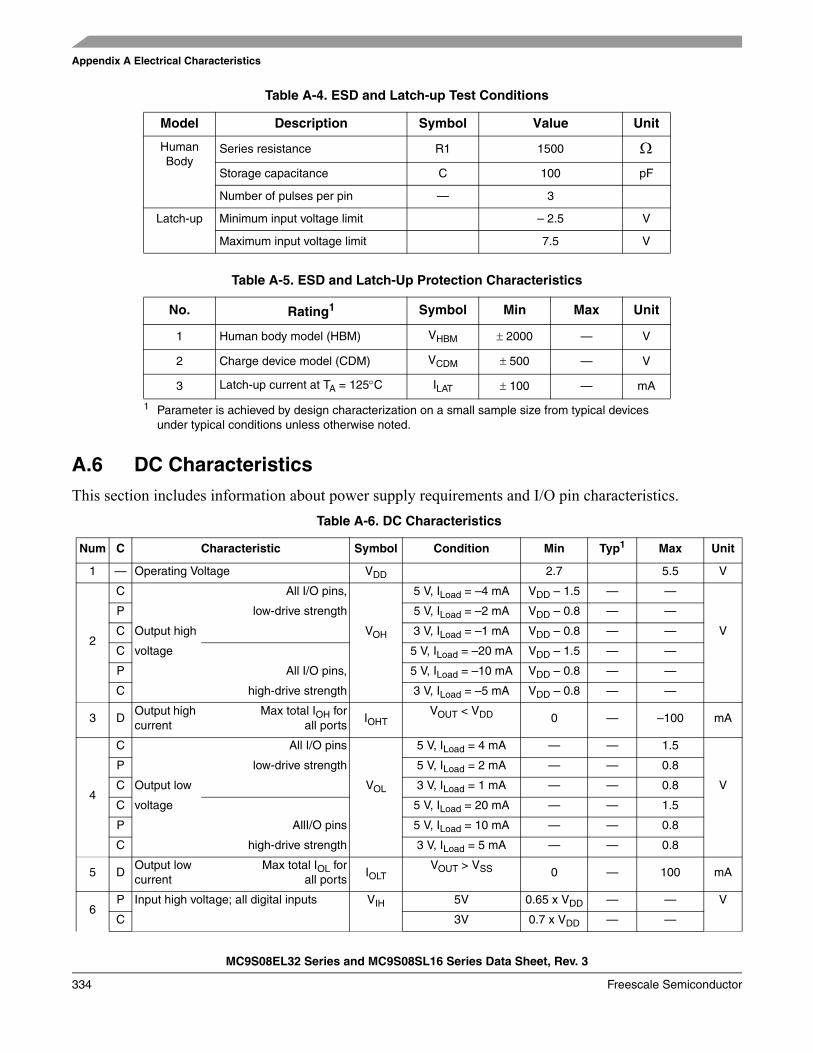
Appendix A Electrical Characteristics
MC9S08EL32 Series and MC9S08SL16 Series Data Sheet, Rev. 3
334 Freescale Semiconductor
A.6 DC CharacteristicsThis section includes information about power supply requirements and I/O pin characteristics.
Table A-4. ESD and Latch-up Test Conditions
Model Description Symbol Value Unit
Human Body
Series resistance R1 1500 ΩStorage capacitance C 100 pF
Number of pulses per pin — 3
Latch-up Minimum input voltage limit – 2.5 V
Maximum input voltage limit 7.5 V
Table A-5. ESD and Latch-Up Protection Characteristics
No. Rating1
1 Parameter is achieved by design characterization on a small sample size from typical devices under typical conditions unless otherwise noted.
Symbol Min Max Unit
1 Human body model (HBM) VHBM ± 2000 — V
2 Charge device model (CDM) VCDM ± 500 — V
3 Latch-up current at TA = 125°C ILAT ± 100 — mA
Table A-6. DC Characteristics
Num C Characteristic Symbol Condition Min Typ1 Max Unit
1 — Operating Voltage VDD 2.7 5.5 V
2
C All I/O pins, 5 V, ILoad = –4 mA VDD – 1.5 — —
P low-drive strength 5 V, ILoad = –2 mA VDD – 0.8 — —
C Output high VOH 3 V, ILoad = –1 mA VDD – 0.8 — — V
C voltage 5 V, ILoad = –20 mA VDD – 1.5 — —
P All I/O pins, 5 V, ILoad = –10 mA VDD – 0.8 — —
C high-drive strength 3 V, ILoad = –5 mA VDD – 0.8 — —
3 DOutput high current
Max total IOH forall ports
IOHTVOUT < VDD 0 — –100 mA
4
C All I/O pins 5 V, ILoad = 4 mA — — 1.5
P low-drive strength 5 V, ILoad = 2 mA — — 0.8
C Output low VOL 3 V, ILoad = 1 mA — — 0.8 V
C voltage 5 V, ILoad = 20 mA — — 1.5
P AllI/O pins 5 V, ILoad = 10 mA — — 0.8
C high-drive strength 3 V, ILoad = 5 mA — — 0.8
5 DOutput low current
Max total IOL forall ports
IOLTVOUT > VSS 0 — 100 mA
6P Input high voltage; all digital inputs VIH 5V 0.65 x VDD — — V
C 3V 0.7 x VDD — —
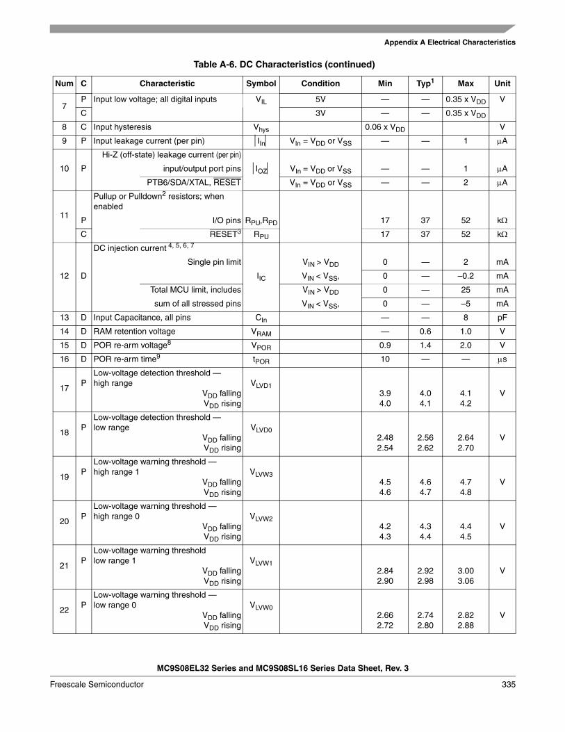
Appendix A Electrical Characteristics
MC9S08EL32 Series and MC9S08SL16 Series Data Sheet, Rev. 3
Freescale Semiconductor 335
7P Input low voltage; all digital inputs VIL 5V — — 0.35 x VDD V
C 3V — — 0.35 x VDD
C Input hysteresis Vhys 0.06 x VDD V8
9 P Input leakage current (per pin) |IIn| VIn = VDD or VSS — — 1 μA
10
Hi-Z (off-state) leakage current (per pin)P input/output port pins |IOZ| VIn = VDD or VSS — — 1 μA
PTB6/SDA/XTAL, RESET VIn = VDD or VSS — — 2 μA
11
Pullup or Pulldown2 resistors; when enabled
P I/O pins RPU,RPD 17 37 52 kΩ
C RESET3 RPU 17 37 52 kΩ
12
DC injection current 4, 5, 6, 7
Single pin limit VIN > VDD 0 — 2 mA
D IIC VIN < VSS, 0 — –0.2 mA
Total MCU limit, includes VIN > VDD 0 — 25 mA
sum of all stressed pins VIN < VSS, 0 — –5 mA
13 D Input Capacitance, all pins CIn — — 8 pF
14 D RAM retention voltage VRAM — 0.6 1.0 V
15 D POR re-arm voltage8 VPOR 0.9 1.4 2.0 V
16 D POR re-arm time9 tPOR 10 — — μs
17P
Low-voltage detection threshold —high range
VDD fallingVDD rising
VLVD13.94.0
4.04.1
4.14.2
V
18P
Low-voltage detection threshold —low range
VDD fallingVDD rising
VLVD02.482.54
2.562.62
2.642.70
V
19P
Low-voltage warning threshold —high range 1
VDD fallingVDD rising
VLVW34.54.6
4.64.7
4.74.8
V
20P
Low-voltage warning threshold —high range 0
VDD fallingVDD rising
VLVW24.24.3
4.34.4
4.44.5
V
21P
Low-voltage warning threshold low range 1
VDD fallingVDD rising
VLVW12.842.90
2.922.98
3.003.06
V
22P
Low-voltage warning threshold —low range 0
VDD fallingVDD rising
VLVW02.662.72
2.742.80
2.822.88
V
Table A-6. DC Characteristics (continued)
Num C Characteristic Symbol Condition Min Typ1 Max Unit
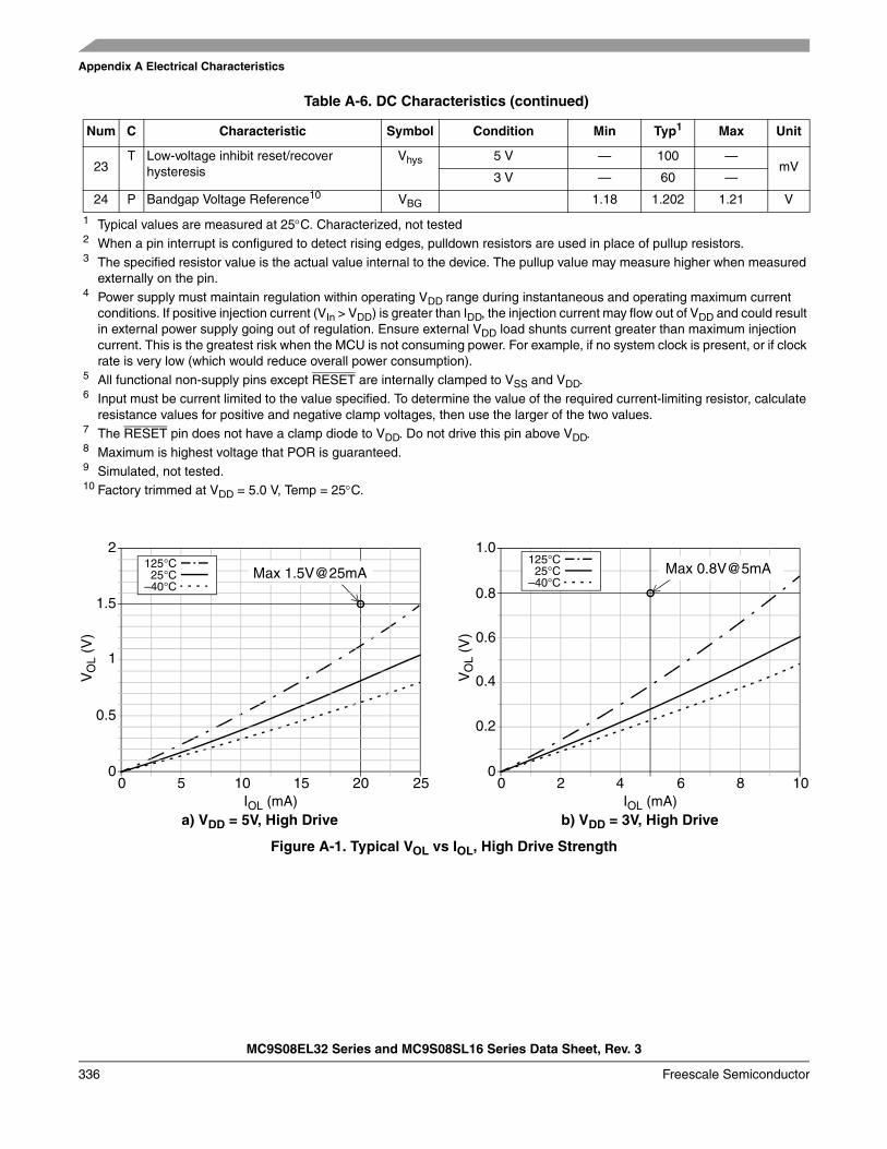
Appendix A Electrical Characteristics
MC9S08EL32 Series and MC9S08SL16 Series Data Sheet, Rev. 3
336 Freescale Semiconductor
Figure A-1. Typical VOL vs IOL, High Drive Strength
23T Low-voltage inhibit reset/recover
hysteresisVhys 5 V — 100 —
mV3 V — 60 —
24 P Bandgap Voltage Reference10 VBG 1.18 1.202 1.21 V
1 Typical values are measured at 25°C. Characterized, not tested2 When a pin interrupt is configured to detect rising edges, pulldown resistors are used in place of pullup resistors.3 The specified resistor value is the actual value internal to the device. The pullup value may measure higher when measured
externally on the pin.4 Power supply must maintain regulation within operating VDD range during instantaneous and operating maximum current
conditions. If positive injection current (VIn > VDD) is greater than IDD, the injection current may flow out of VDD and could result in external power supply going out of regulation. Ensure external VDD load shunts current greater than maximum injection current. This is the greatest risk when the MCU is not consuming power. For example, if no system clock is present, or if clock rate is very low (which would reduce overall power consumption).
5 All functional non-supply pins except RESET are internally clamped to VSS and VDD.6 Input must be current limited to the value specified. To determine the value of the required current-limiting resistor, calculate
resistance values for positive and negative clamp voltages, then use the larger of the two values.7 The RESET pin does not have a clamp diode to VDD. Do not drive this pin above VDD.8 Maximum is highest voltage that POR is guaranteed.9 Simulated, not tested.10 Factory trimmed at VDD = 5.0 V, Temp = 25°C.
Table A-6. DC Characteristics (continued)
Num C Characteristic Symbol Condition Min Typ1 Max Unit
VO
L (V
)
IOL (mA)20151050 25
0
0.5
1
1.5
2
a) VDD = 5V, High Drive
VO
L (V
)
IOL (mA)86420 10
0
0.2
0.4
0.8
1.0
b) VDD = 3V, High Drive
0.6
125°C25°C
–40°CMax 0.8V@5mAMax 1.5V@25mA
125°C25°C
–40°C
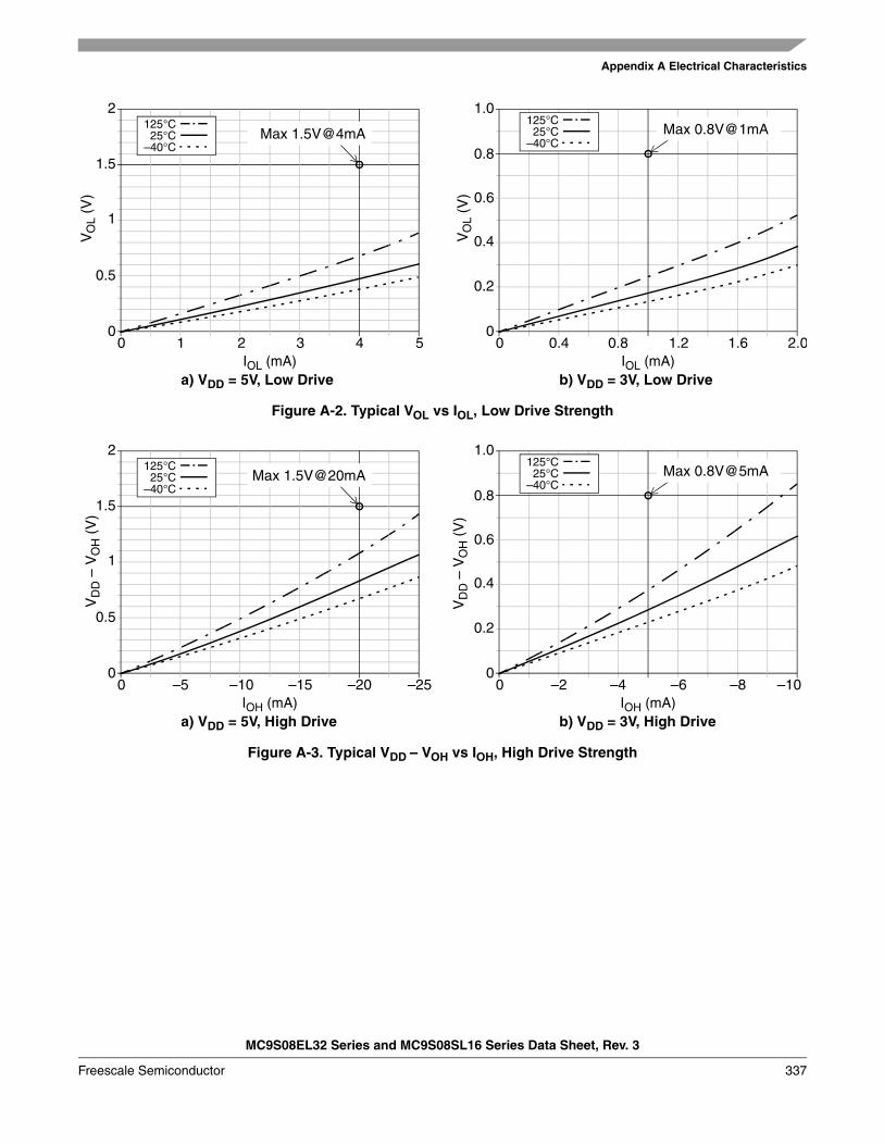
Appendix A Electrical Characteristics
MC9S08EL32 Series and MC9S08SL16 Series Data Sheet, Rev. 3
Freescale Semiconductor 337
Figure A-2. Typical VOL vs IOL, Low Drive Strength
Figure A-3. Typical VDD – VOH vs IOH, High Drive Strength
VO
L (V
)
IOL (mA)43210 5
0
0.5
1
1.5
2125°C25°C
–40°C
a) VDD = 5V, Low Drive
VO
L (V
)
IOL (mA)1.61.20.80.40 2.0
0
0.2
0.4
0.8
1.0
b) VDD = 3V, Low Drive
0.6
125°C25°C
–40°CMax 0.8V@1mAMax 1.5V@4mA
IOH (mA)–20–15–10–50 –25
0
0.5
1
1.5
2125°C25°C
–40°C
a) VDD = 5V, High DriveIOH (mA)
–8–6–4–20 –100
0.2
0.4
0.8
1.0
b) VDD = 3V, High Drive
0.6
125°C25°C
–40°CMax 0.8V@5mAMax 1.5V@20mA
VD
D –
VO
H (
V)
VD
D –
VO
H (
V)
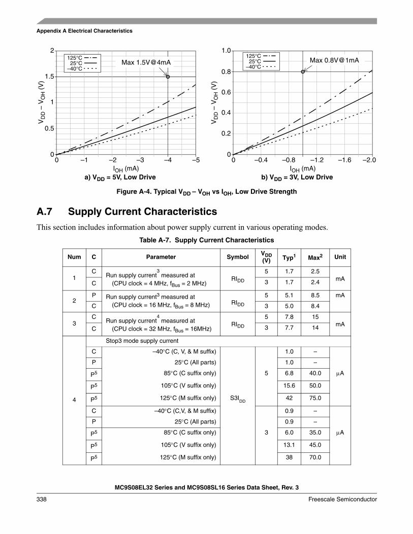
Appendix A Electrical Characteristics
MC9S08EL32 Series and MC9S08SL16 Series Data Sheet, Rev. 3
338 Freescale Semiconductor
Figure A-4. Typical VDD – VOH vs IOH, Low Drive Strength
A.7 Supply Current CharacteristicsThis section includes information about power supply current in various operating modes.
Table A-7. Supply Current Characteristics
Num C Parameter Symbol VDD (V) Typ1 Max2 Unit
1C
Run supply current3 measured at
(CPU clock = 4 MHz, fBus = 2 MHz)RIDD
5 1.7 2.5mA
C 3 1.7 2.4
2P Run supply current3 measured at
(CPU clock = 16 MHz, fBus = 8 MHz) RIDD
5 5.1 8.5 mA
C 3 5.0 8.4
3C
Run supply current4 measured at
(CPU clock = 32 MHz, fBus = 16MHz)RIDD
5 7.8 15mA
C 3 7.7 14
4
Stop3 mode supply current
C –40°C (C, V, & M suffix) 1.0 –
P 25°C (All parts) 1.0 –
P5 85°C (C suffix only) 5 6.8 40.0 μA
P5 105°C (V suffix only) 15.6 50.0
P5 125°C (M suffix only) S3IDD
42 75.0
C –40°C (C,V, & M suffix) 0.9 –
P 25°C (All parts) 0.9 –
P5 85°C (C suffix only) 3 6.0 35.0 μA
P5 105°C (V suffix only) 13.1 45.0
P5 125°C (M suffix only) 38 70.0
VD
D –
VO
H (
V)
IOH (mA)–4–3–2–10 –5
0
0.5
1
1.5
2125°C25°C
–40°C
a) VDD = 5V, Low DriveIOH (mA)
–1.6–1.2–0.8–0.40 –2.00
0.2
0.4
0.8
1.0
b) VDD = 3V, Low Drive
0.6
125°C25°C
–40°CMax 0.8V@1mAMax 1.5V@4mA
VD
D –
VO
H (
V)
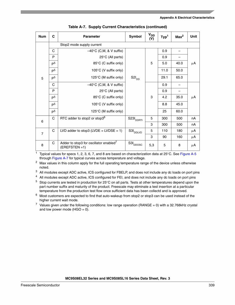
Appendix A Electrical Characteristics
MC9S08EL32 Series and MC9S08SL16 Series Data Sheet, Rev. 3
Freescale Semiconductor 339
5
Stop2 mode supply current
C –40°C (C,M, & V suffix) 0.9 –
P 25°C (All parts) 0.9 –
P5 85°C (C suffix only) 5 5.0 40.0 μA
P5 105°C (V suffix only) 11.0 50.0
P5 125°C (M suffix only) S2IDD
29.1 65.0
C –40°C (C,M, & V suffix) 0.9 –
P 25°C (All parts) 0.9 –
P5 85°C (C suffix only) 3 4.2 35.0 μA
P5 105°C (V suffix only) 8.8 45.0
P5 125°C (M suffix only) 25 60.0
6C RTC adder to stop2 or stop36 S23I
DDRTI5 300 500 nA
3 300 500 nA
7C LVD adder to stop3 (LVDE = LVDSE = 1) S3I
DDLVD5 110 180 μA
3 90 160 μA
8C Adder to stop3 for oscillator enabled7
(EREFSTEN =1)S3I
DDOSC 5,3 5 8 μA
1 Typical values for specs 1, 2, 3, 6, 7, and 8 are based on characterization data at 25°C. See Figure A-5 through Figure A-7 for typical curves across temperature and voltage.
2 Max values in this column apply for the full operating temperature range of the device unless otherwise noted.
3 All modules except ADC active, ICS configured for FBELP, and does not include any dc loads on port pins4 All modules except ADC active, ICS configured for FEI, and does not include any dc loads on port pins5 Stop currents are tested in production for 25°C on all parts. Tests at other temperatures depend upon the
part number suffix and maturity of the product. Freescale may eliminate a test insertion at a particular temperature from the production test flow once sufficient data has been collectd and is approved.
6 Most customers are expected to find that auto-wakeup from stop2 or stop3 can be used instead of the higher current wait mode.
7 Values given under the following conditions: low range operation (RANGE = 0) with a 32.768kHz crystal and low power mode (HGO = 0).
Table A-7. Supply Current Characteristics (continued)
Num C Parameter Symbol VDD (V) Typ1 Max2 Unit
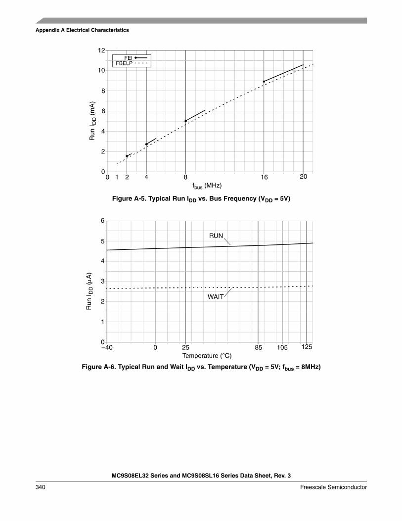
Appendix A Electrical Characteristics
MC9S08EL32 Series and MC9S08SL16 Series Data Sheet, Rev. 3
340 Freescale Semiconductor
Figure A-5. Typical Run IDD vs. Bus Frequency (VDD = 5V)
Figure A-6. Typical Run and Wait IDD vs. Temperature (VDD = 5V; fbus = 8MHz)
Run
I DD
(m
A)
fbus (MHz)84210 16
0
2
4
10
20
6
8
FEIFBELP
12
Run
I DD
(μA
)
Temperature (°C)85250–40 105
0
1
2
5
125
3
4
RUN
WAIT
6
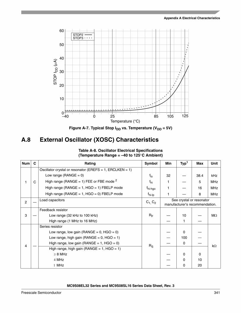
Appendix A Electrical Characteristics
MC9S08EL32 Series and MC9S08SL16 Series Data Sheet, Rev. 3
Freescale Semiconductor 341
Figure A-7. Typical Stop IDD vs. Temperature (VDD = 5V)
A.8 External Oscillator (XOSC) Characteristics
Table A-8. Oscillator Electrical Specifications(Temperature Range = –40 to 125°C Ambient)
Num C Rating Symbol Min Typ1 Max Unit
1 C
Oscillator crystal or resonator (EREFS = 1, ERCLKEN = 1)
Low range (RANGE = 0) flo 32 — 38.4 kHz
High range (RANGE = 1) FEE or FBE mode 2 fhi 1 — 5 MHz
High range (RANGE = 1, HGO = 1) FBELP mode fhi-hgo 1 — 16 MHz
High range (RANGE = 1, HGO = 0) FBELP mode fhi-lp 1 — 8 MHz
2 —Load capacitors C1, C2
See crystal or resonator manufacturer’s recommendation.
3 —
Feedback resistor
RF MΩLow range (32 kHz to 100 kHz) — 10 —
High range (1 MHz to 16 MHz) — 1 —
4 —
Series resistor
RS kΩ
Low range, low gain (RANGE = 0, HGO = 0) — 0 —
Low range, high gain (RANGE = 0, HGO = 1) — 100 —
High range, low gain (RANGE = 1, HGO = 0) — 0 —
High range, high gain (RANGE = 1, HGO = 1)
≥ 8 MHz — 0 0
4 MHz — 0 10
1 MHz — 0 20
STO
P I D
D (
μA)
Temperature (°C)85250–40 105
0
10
20
50
125
30
40
60STOP2STOP3
Appendix A Electrical Characteristics
MC9S08EL32 Series and MC9S08SL16 Series Data Sheet, Rev. 3
342 Freescale Semiconductor
A.9 Internal Clock Source (ICS) Characteristics
5 T
Crystal start-up time 3
ms
Low range, low gain (RANGE = 0, HGO = 0) tCSTL-LP — 200 —
Low range, high gain (RANGE = 0, HGO = 1) tCSTL-HGO — 400 —
High range, low gain (RANGE = 1, HGO = 0)4 tCSTH-LP — 5 —
High range, high gain (RANGE = 1, HGO = 1)4 tCSTH-HGO — 20 —
6 T
Square wave input clock frequency (EREFS = 0, ERCLKEN = 1)
fextalFEE or FBE mode 2 0.03125 — 5 MHz
FBELP mode 0 — 40 MHz1 Typical data was characterized at 5.0 V, 25°C or is recommended value.2 The input clock source must be divided using RDIV to within the range of 31.25 kHz to 39.0625 kHz.3 Characterized and not tested on each device. Proper PC board layout procedures must be followed to achieve specifications.4 4 MHz crystal
Table A-9. ICS Frequency Specifications(Temperature Range = –40 to 125°C Ambient)
Num C Rating Symbol Min Typical Max Unit
1 PInternal reference frequency — factory trimmed at VDD
= 5 V and temperature = 25°Cfint_ft — 31.25 — kHz
2 T Internal reference frequency — untrimmed1 fint_ut 25 36 41.66 kHz
3 P Internal reference frequency — trimmed fint_t 31.25 — 39.0625 kHz
4 D Internal reference startup time tirefst — 55 100 μs
5 — DCO output frequency range — untrimmed1 value provided for reference: fdco_ut = 1024 x fint_ut
fdco_ut 25.6 36.86 42.66 MHz
6 D DCO output frequency range — trimmed fdco_t 32 — 40 MHz
7 DResolution of trimmed DCO output frequency at fixed voltage and temperature (using FTRIM)
Δfdco_res_t — ± 0.1 ± 0.2 %fdco
8 DResolution of trimmed DCO output frequency at fixed voltage and temperature (not using FTRIM)
Δfdco_res_t — ± 0.2 ± 0.4 %fdco
Table A-8. Oscillator Electrical Specifications(Temperature Range = –40 to 125°C Ambient) (continued)
Num C Rating Symbol Min Typ1 Max Unit
MCUEXTAL XTAL
Crystal or Resonator
RS
C2
RF
C1
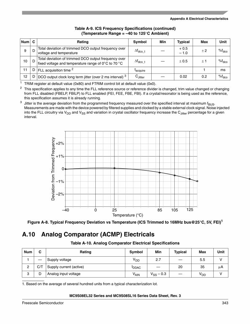
Appendix A Electrical Characteristics
MC9S08EL32 Series and MC9S08SL16 Series Data Sheet, Rev. 3
Freescale Semiconductor 343
Figure A-8. Typical Frequency Deviation vs Temperature (ICS Trimmed to 16MHz bus@25°C, 5V, FEI)1
A.10 Analog Comparator (ACMP) Electricals
9 DTotal deviation of trimmed DCO output frequency over voltage and temperature
Δfdco_t —+ 0.5– 1.0
± 2 %fdco
10 DTotal deviation of trimmed DCO output frequency over fixed voltage and temperature range of 0°C to 70 °C
Δfdco_t — ± 0.5 ± 1 %fdco
11 D FLL acquisition time 2 tacquire 1 ms
12 D DCO output clock long term jitter (over 2 ms interval) 3 CJitter — 0.02 0.2 %fdco
1 TRIM register at default value (0x80) and FTRIM control bit at default value (0x0).2 This specification applies to any time the FLL reference source or reference divider is changed, trim value changed or changing
from FLL disabled (FBELP, FBILP) to FLL enabled (FEI, FEE, FBE, FBI). If a crystal/resonator is being used as the reference, this specification assumes it is already running.
3 Jitter is the average deviation from the programmed frequency measured over the specified interval at maximum fBUS. Measurements are made with the device powered by filtered supplies and clocked by a stable external clock signal. Noise injected into the FLL circuitry via VDD and VSS and variation in crystal oscillator frequency increase the CJitter percentage for a given interval.
1. Based on the average of several hundred units from a typical characterization lot.
Table A-10. Analog Comparator Electrical Specifications
Num C Rating Symbol Min Typical Max Unit
1 — Supply voltage VDD 2.7 — 5.5 V
2 C/T Supply current (active) IDDAC — 20 35 μA
3 D Analog input voltage VAIN VSS – 0.3 — VDD V
Table A-9. ICS Frequency Specifications (continued)(Temperature Range = –40 to 125°C Ambient)
Num C Rating Symbol Min Typical Max Unit
Dev
iatio
n fr
om T
rimm
ed F
requ
ency
Temperature (°C)85250–40 105
–2%
–1%
+2%
125
+1%
0
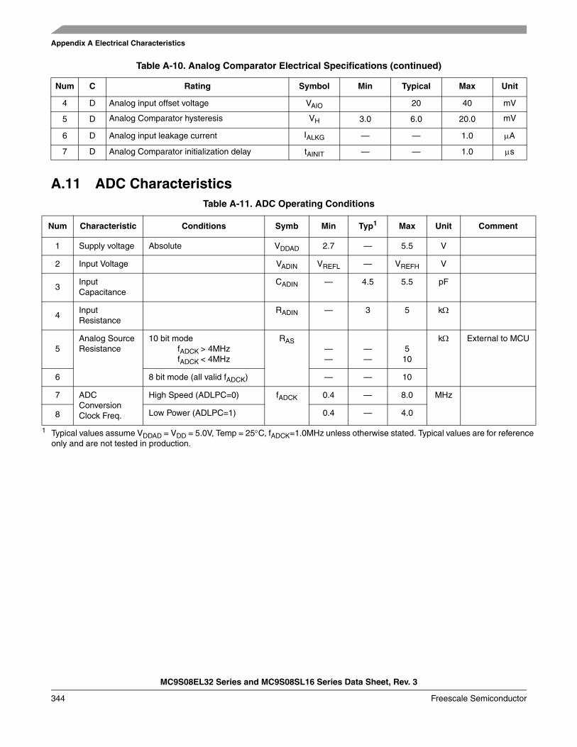
Appendix A Electrical Characteristics
MC9S08EL32 Series and MC9S08SL16 Series Data Sheet, Rev. 3
344 Freescale Semiconductor
A.11 ADC Characteristics
4 D Analog input offset voltage VAIO 20 40 mV
5 D Analog Comparator hysteresis VH 3.0 6.0 20.0 mV
6 D Analog input leakage current IALKG — — 1.0 μA
7 D Analog Comparator initialization delay tAINIT — — 1.0 μs
Table A-11. ADC Operating Conditions
Num Characteristic Conditions Symb Min Typ1
1 Typical values assume VDDAD = VDD = 5.0V, Temp = 25°C, fADCK=1.0MHz unless otherwise stated. Typical values are for reference only and are not tested in production.
Max Unit Comment
1 Supply voltage Absolute VDDAD 2.7 — 5.5 V
2 Input Voltage VADIN VREFL — VREFH V
3Input Capacitance
CADIN — 4.5 5.5 pF
4Input Resistance
RADIN — 3 5 kΩ
5Analog Source Resistance
10 bit modefADCK > 4MHzfADCK < 4MHz
RAS——
——
510
kΩ External to MCU
6 8 bit mode (all valid fADCK) — — 10
7 ADC Conversion Clock Freq.
High Speed (ADLPC=0) fADCK 0.4 — 8.0 MHz
8 Low Power (ADLPC=1) 0.4 — 4.0
Table A-10. Analog Comparator Electrical Specifications (continued)
Num C Rating Symbol Min Typical Max Unit
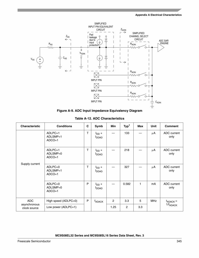
Appendix A Electrical Characteristics
MC9S08EL32 Series and MC9S08SL16 Series Data Sheet, Rev. 3
Freescale Semiconductor 345
Figure A-9. ADC Input Impedance Equivalency Diagram
Table A-12. ADC Characteristics
Characteristic Conditions C Symb Min Typ1 Max Unit Comment
Supply current
ADLPC=1ADLSMP=1ADCO=1
T IDD + IDDAD
— 133 — μA ADC current only
ADLPC=1ADLSMP=0ADCO=1
T IDD + IDDAD
— 218 — μA ADC current only
ADLPC=0ADLSMP=1ADCO=1
T IDD + IDDAD
— 327 — μA ADC current only
ADLPC=0ADLSMP=0ADCO=1
P IDD + IDDAD
— 0.582 1 mA ADC current only
ADC asynchronous clock source
High speed (ADLPC=0) P fADACK 2 3.3 5 MHz tADACK =1/fADACK
Low power (ADLPC=1) 1.25 2 3.3
+–
+
–VAS
RAS
CAS
VADIN
ZASPad leakagedue toinput protection
ZADIN
SIMPLIFIED INPUT PIN EQUIVALENT
CIRCUIT
RADIN
ADC SARENGINE
SIMPLIFIED CHANNEL SELECT
CIRCUIT
INPUT PIN
RADIN
CADIN
INPUT PIN
RADIN
INPUT PIN
RADIN
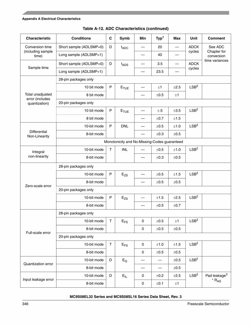
Appendix A Electrical Characteristics
MC9S08EL32 Series and MC9S08SL16 Series Data Sheet, Rev. 3
346 Freescale Semiconductor
Conversion time (including sample
time)
Short sample (ADLSMP=0) D tADC — 20 — ADCK cycles
See ADC Chapter for conversion
time variances
Long sample (ADLSMP=1) — 40 —
Sample timeShort sample (ADLSMP=0) D tADS — 3.5 — ADCK
cyclesLong sample (ADLSMP=1) — 23.5 —
Total unadjusted error (includes quantization)
28-pin packages only
10 bit mode P ETUE — ±1 ±2.5 LSB2
8 bit mode — ±0.5 ±1
20-pin packages only
10 bit mode P ETUE — ±.5 ±3.5 LSB2
8 bit mode — ±0.7 ±1.5
Differential Non-Linearity
10-bit mode P DNL — ±0.5 ±1.0 LSB2
8-bit mode — ±0.3 ±0.5
Monotonicity and No-Missing-Codes guaranteed
Integral non-linearity
10-bit mode T INL — ±0.5 ±1.0 LSB2
8-bit mode — ±0.3 ±0.5
Zero-scale error
28-pin packages only
10-bit mode P EZS — ±0.5 ±1.5 LSB2
8-bit mode — ±0.5 ±0.5
20-pin packages only
10-bit mode P EZS — ±1.5 ±2.5 LSB2
8-bit mode — ±0.5 ±0.7
Full-scale error
28-pin packages only
10-bit mode T EFS 0 ±0.5 ±1 LSB2
8-bit mode 0 ±0.5 ±0.5
20-pin packages only
10-bit mode T EFS 0 ±1.0 ±1.5 LSB2
8-bit mode 0 ±0.5 ±0.5
Quantization error10-bit mode D EQ — — ±0.5 LSB2
8-bit mode — — ±0.5
Input leakage error10-bit mode D EIL 0 ±0.2 ±2.5 LSB2 Pad leakage3
* RAS8-bit mode 0 ±0.1 ±1
Table A-12. ADC Characteristics (continued)
Characteristic Conditions C Symb Min Typ1 Max Unit Comment
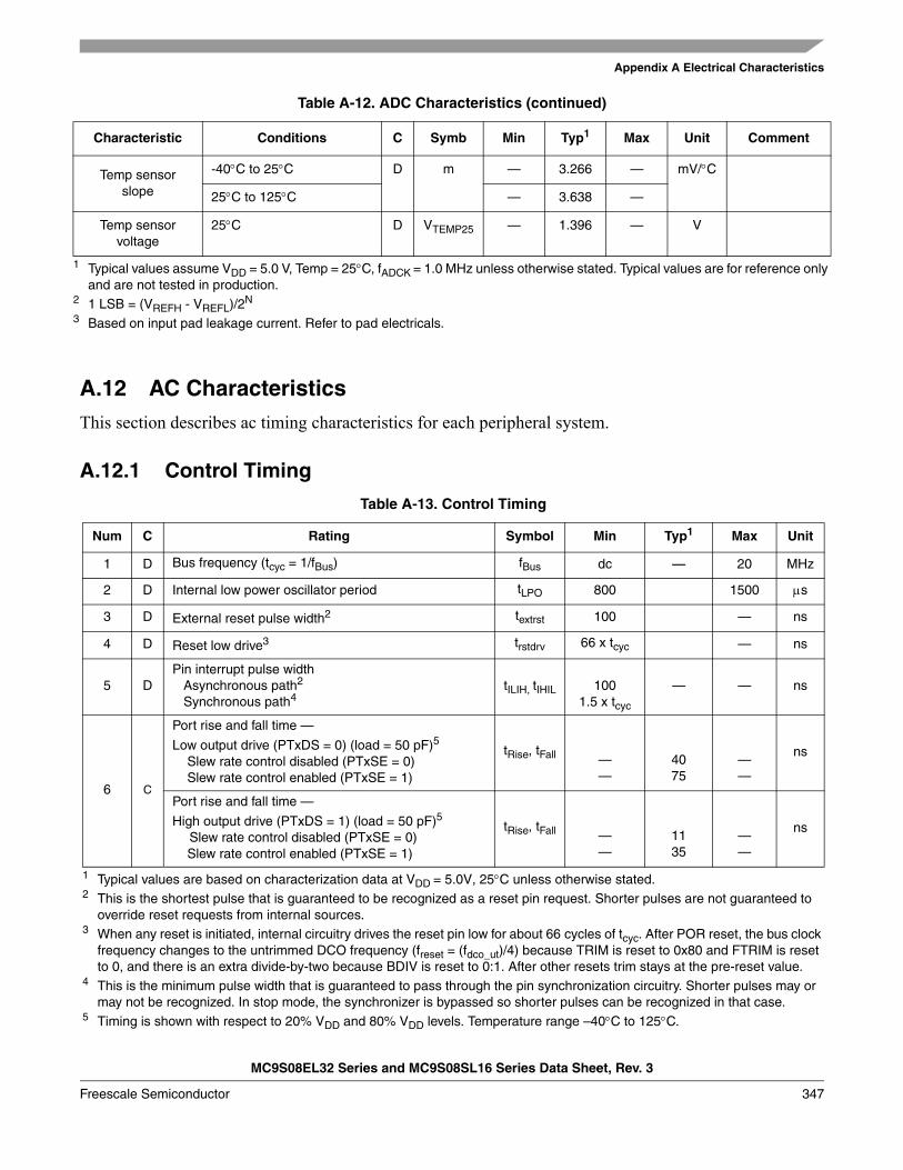
Appendix A Electrical Characteristics
MC9S08EL32 Series and MC9S08SL16 Series Data Sheet, Rev. 3
Freescale Semiconductor 347
A.12 AC CharacteristicsThis section describes ac timing characteristics for each peripheral system.
A.12.1 Control Timing
Temp sensorslope
-40°C to 25°C D m — 3.266 — mV/°C
25°C to 125°C — 3.638 —
Temp sensorvoltage
25°C D VTEMP25 — 1.396 — V
1 Typical values assume VDD = 5.0 V, Temp = 25°C, fADCK = 1.0 MHz unless otherwise stated. Typical values are for reference only and are not tested in production.
2 1 LSB = (VREFH - VREFL)/2N
3 Based on input pad leakage current. Refer to pad electricals.
Table A-13. Control Timing
Num C Rating Symbol Min Typ1
1 Typical values are based on characterization data at VDD = 5.0V, 25°C unless otherwise stated.
Max Unit
1 D Bus frequency (tcyc = 1/fBus) fBus dc — 20 MHz
2 D Internal low power oscillator period tLPO 800 1500 μs
3 D External reset pulse width2
2 This is the shortest pulse that is guaranteed to be recognized as a reset pin request. Shorter pulses are not guaranteed to override reset requests from internal sources.
textrst 100 — ns
4 D Reset low drive3
3 When any reset is initiated, internal circuitry drives the reset pin low for about 66 cycles of tcyc. After POR reset, the bus clock frequency changes to the untrimmed DCO frequency (freset = (fdco_ut)/4) because TRIM is reset to 0x80 and FTRIM is reset to 0, and there is an extra divide-by-two because BDIV is reset to 0:1. After other resets trim stays at the pre-reset value.
trstdrv 66 x tcyc — ns
5 DPin interrupt pulse width
Asynchronous path2
Synchronous path4
4 This is the minimum pulse width that is guaranteed to pass through the pin synchronization circuitry. Shorter pulses may or may not be recognized. In stop mode, the synchronizer is bypassed so shorter pulses can be recognized in that case.
tILIH, tIHIL 1001.5 x tcyc
— — ns
6 C
Port rise and fall time —
Low output drive (PTxDS = 0) (load = 50 pF)5
Slew rate control disabled (PTxSE = 0) Slew rate control enabled (PTxSE = 1)
5 Timing is shown with respect to 20% VDD and 80% VDD levels. Temperature range –40°C to 125°C.
tRise, tFall ——
4075
——
ns
Port rise and fall time —
High output drive (PTxDS = 1) (load = 50 pF)5
Slew rate control disabled (PTxSE = 0) Slew rate control enabled (PTxSE = 1)
tRise, tFall ——
1135
——
ns
Table A-12. ADC Characteristics (continued)
Characteristic Conditions C Symb Min Typ1 Max Unit Comment
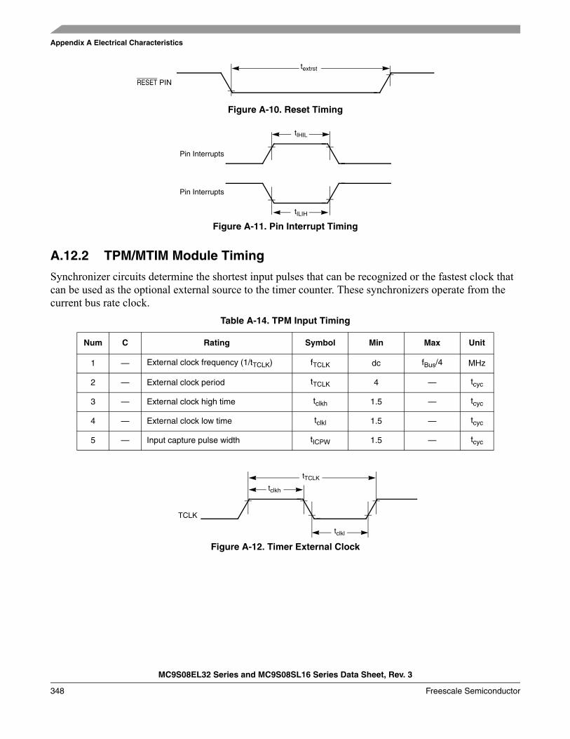
Appendix A Electrical Characteristics
MC9S08EL32 Series and MC9S08SL16 Series Data Sheet, Rev. 3
348 Freescale Semiconductor
Figure A-10. Reset Timing
Figure A-11. Pin Interrupt Timing
A.12.2 TPM/MTIM Module Timing
Synchronizer circuits determine the shortest input pulses that can be recognized or the fastest clock that can be used as the optional external source to the timer counter. These synchronizers operate from the current bus rate clock.
Figure A-12. Timer External Clock
Table A-14. TPM Input Timing
Num C Rating Symbol Min Max Unit
1 — External clock frequency (1/tTCLK) fTCLK dc fBus/4 MHz
2 — External clock period tTCLK 4 — tcyc
3 — External clock high time tclkh 1.5 — tcyc
4 — External clock low time tclkl 1.5 — tcyc
5 — Input capture pulse width tICPW 1.5 — tcyc
textrst
RESET PIN
tIHIL
Pin Interrupts
tILIH
Pin Interrupts
tTCLK
tclkh
tclkl
TCLK
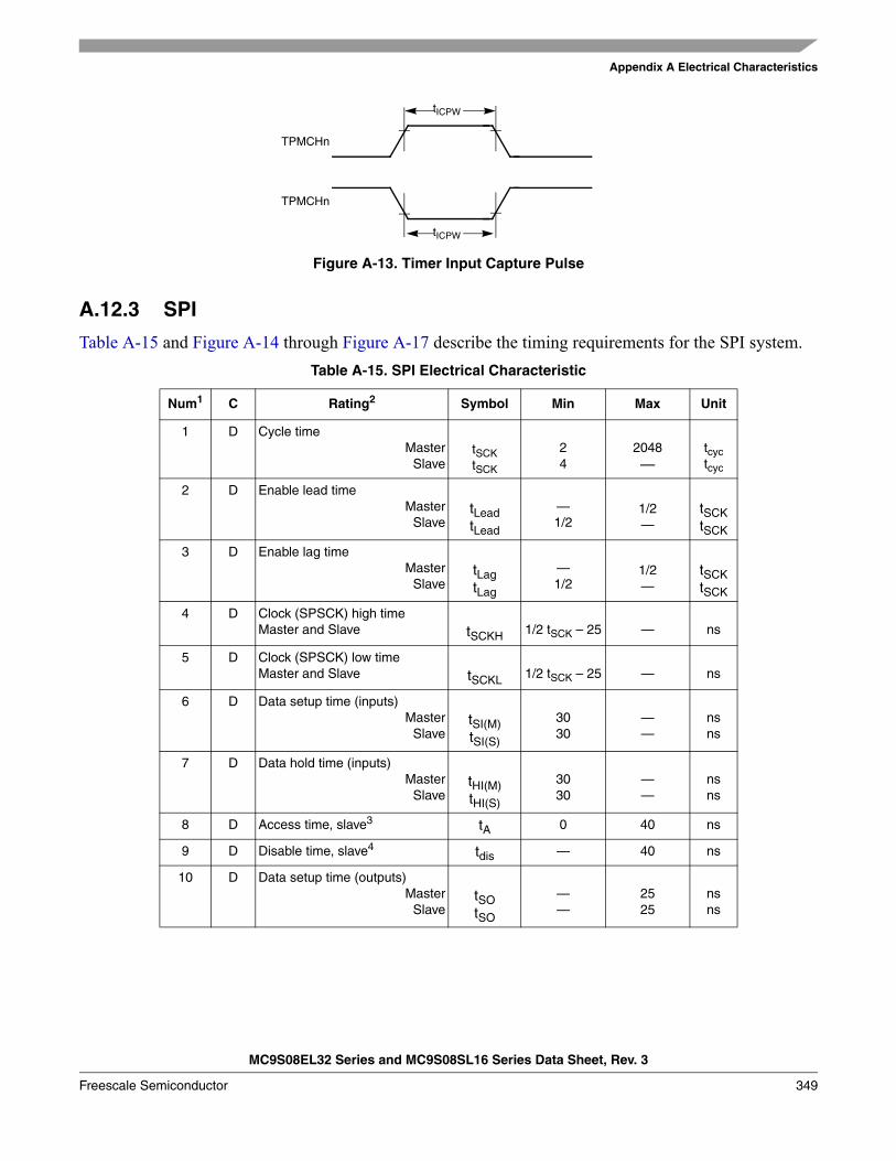
Appendix A Electrical Characteristics
MC9S08EL32 Series and MC9S08SL16 Series Data Sheet, Rev. 3
Freescale Semiconductor 349
Figure A-13. Timer Input Capture Pulse
A.12.3 SPI
Table A-15 and Figure A-14 through Figure A-17 describe the timing requirements for the SPI system.Table A-15. SPI Electrical Characteristic
Num1 C Rating2 Symbol Min Max Unit
1 D Cycle timeMaster
SlavetSCKtSCK
24
2048—
tcyctcyc
2 D Enable lead timeMaster
SlavetLeadtLead
—1/2
1/2—
tSCKtSCK
3 D Enable lag timeMaster
SlavetLagtLag
—1/2
1/2—
tSCKtSCK
4 D Clock (SPSCK) high timeMaster and Slave tSCKH 1/2 tSCK – 25 — ns
5 D Clock (SPSCK) low time Master and Slave tSCKL 1/2 tSCK – 25 — ns
6 D Data setup time (inputs)Master
SlavetSI(M)tSI(S)
3030
——
nsns
7 D Data hold time (inputs)Master
SlavetHI(M)tHI(S)
3030
——
nsns
8 D Access time, slave3 tA 0 40 ns
9 D Disable time, slave4 tdis — 40 ns
10 D Data setup time (outputs)Master
SlavetSOtSO
——
2525
nsns
tICPW
TPMCHn
tICPW
TPMCHn
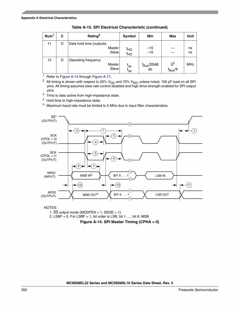
Appendix A Electrical Characteristics
MC9S08EL32 Series and MC9S08SL16 Series Data Sheet, Rev. 3
350 Freescale Semiconductor
Figure A-14. SPI Master Timing (CPHA = 0)
11 D Data hold time (outputs)Master
SlavetHOtHO
–10–10
——
nsns
12 D Operating frequencyMaster
Slavefopfop
fBus/2048dc
55
fBus/4MHz
1 Refer to Figure A-14 through Figure A-17.2 All timing is shown with respect to 20% VDD and 70% VDD, unless noted; 100 pF load on all SPI
pins. All timing assumes slew rate control disabled and high drive strength enabled for SPI output pins.
3 Time to data active from high-impedance state.4 Hold time to high-impedance state.5 Maximum baud rate must be limited to 5 MHz due to input filter characteristics.
Table A-15. SPI Electrical Characteristic (continued)
Num1 C Rating2 Symbol Min Max Unit
SCK
(OUTPUT)
SCK
(OUTPUT)
MISO(INPUT)
MOSI(OUTPUT)
SS1
(OUTPUT)
MSB IN2
BIT 6 . . . 1
LSB IN
MSB OUT2 LSB OUT
BIT 6 . . . 1
(CPOL = 0)
(CPOL = 1)
NOTES:
2. LSBF = 0. For LSBF = 1, bit order is LSB, bit 1, ..., bit 6, MSB.1. SS output mode (MODFEN = 1, SSOE = 1).
12 3
5
6 7
10 11
5
10
4
4
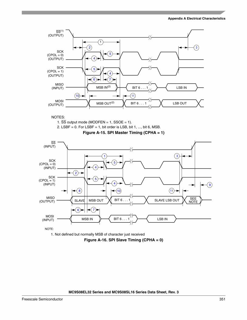
Appendix A Electrical Characteristics
MC9S08EL32 Series and MC9S08SL16 Series Data Sheet, Rev. 3
Freescale Semiconductor 351
Figure A-15. SPI Master Timing (CPHA = 1)
Figure A-16. SPI Slave Timing (CPHA = 0)
SCK
(OUTPUT)
SCK
(OUTPUT)
MISO(INPUT)
MOSI(OUTPUT)
MSB IN(2)
BIT 6 . . . 1
LSB IN
MSB OUT(2) LSB OUT
BIT 6 . . . 1
(CPOL = 0)
(CPOL = 1)
SS(1)
(OUTPUT)
1. SS output mode (MODFEN = 1, SSOE = 1).2. LSBF = 0. For LSBF = 1, bit order is LSB, bit 1, ..., bit 6, MSB.
NOTES:
2
1
3
45
6 7
10 11
54
SCK
(INPUT)
SCK
(INPUT)
MOSI(INPUT)
MISO(OUTPUT)
SS(INPUT)
MSB IN
BIT 6 . . . 1
LSB IN
MSB OUT SLAVE LSB OUT
BIT 6 . . . 1
(CPOL = 0)
(CPOL = 1)
NOTE:
SLAVESEE
NOTE
1. Not defined but normally MSB of character just received
1
2
3
4
6 7
8
9
10 11
5
54
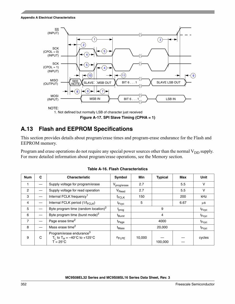
Appendix A Electrical Characteristics
MC9S08EL32 Series and MC9S08SL16 Series Data Sheet, Rev. 3
352 Freescale Semiconductor
Figure A-17. SPI Slave Timing (CPHA = 1)
A.13 Flash and EEPROM SpecificationsThis section provides details about program/erase times and program-erase endurance for the Flash and EEPROM memory.
Program and erase operations do not require any special power sources other than the normal VDD supply. For more detailed information about program/erase operations, see the Memory section.
Table A-16. Flash Characteristics
Num C Characteristic Symbol Min Typical Max Unit
1 — Supply voltage for program/erase Vprog/erase 2.7 5.5 V
2 — Supply voltage for read operation VRead 2.7 5.5 V
3 — Internal FCLK frequency1 fFCLK 150 200 kHz
4 — Internal FCLK period (1/fFCLK) tFcyc 5 6.67 μs
5 — Byte program time (random location)2 tprog 9 tFcyc
6 — Byte program time (burst mode)2 tBurst 4 tFcyc
7 — Page erase time2 tPage 4000 tFcyc
8 — Mass erase time2 tMass 20,000 tFcyc
9 CProgram/erase endurance3
TL to TH = –40°C to +125°CT = 25°C
nFLPE 10,000 —100,000
——
cycles
SCK
(INPUT)
SCK
(INPUT)
MOSI(INPUT)
MISO(OUTPUT)
MSB IN
BIT 6 . . . 1
LSB IN
MSB OUT SLAVE LSB OUT
BIT 6 . . . 1
SEE
(CPOL = 0)
(CPOL = 1)
SS(INPUT)
NOTE:
SLAVE NOTE
1. Not defined but normally LSB of character just received
1
2
3
4
6 78
910 11
45
5
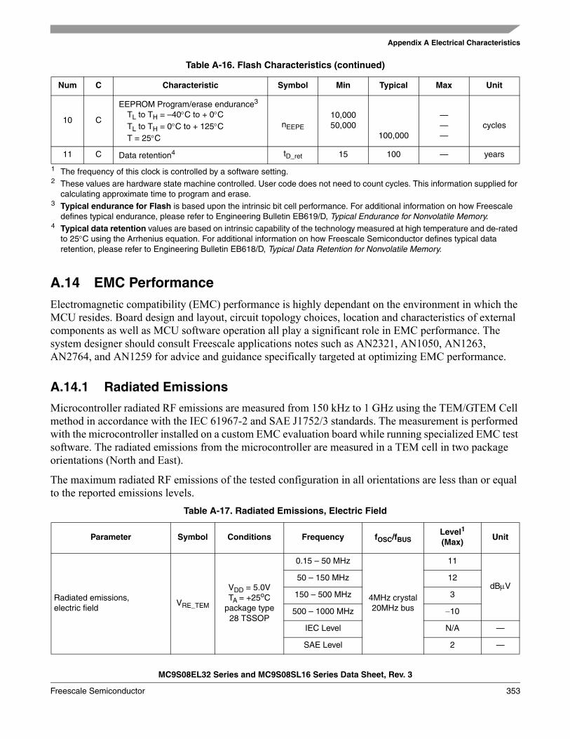
Appendix A Electrical Characteristics
MC9S08EL32 Series and MC9S08SL16 Series Data Sheet, Rev. 3
Freescale Semiconductor 353
A.14 EMC PerformanceElectromagnetic compatibility (EMC) performance is highly dependant on the environment in which the MCU resides. Board design and layout, circuit topology choices, location and characteristics of external components as well as MCU software operation all play a significant role in EMC performance. The system designer should consult Freescale applications notes such as AN2321, AN1050, AN1263, AN2764, and AN1259 for advice and guidance specifically targeted at optimizing EMC performance.
A.14.1 Radiated Emissions
Microcontroller radiated RF emissions are measured from 150 kHz to 1 GHz using the TEM/GTEM Cell method in accordance with the IEC 61967-2 and SAE J1752/3 standards. The measurement is performed with the microcontroller installed on a custom EMC evaluation board while running specialized EMC test software. The radiated emissions from the microcontroller are measured in a TEM cell in two package orientations (North and East).
The maximum radiated RF emissions of the tested configuration in all orientations are less than or equal to the reported emissions levels.
10 C
EEPROM Program/erase endurance3
TL to TH = –40°C to + 0°CTL to TH = 0°C to + 125°CT = 25°C
nEEPE
10,00050,000
100,000
———
cycles
11 C Data retention4 tD_ret 15 100 — years
1 The frequency of this clock is controlled by a software setting.2 These values are hardware state machine controlled. User code does not need to count cycles. This information supplied for
calculating approximate time to program and erase.3 Typical endurance for Flash is based upon the intrinsic bit cell performance. For additional information on how Freescale
defines typical endurance, please refer to Engineering Bulletin EB619/D, Typical Endurance for Nonvolatile Memory.4 Typical data retention values are based on intrinsic capability of the technology measured at high temperature and de-rated
to 25°C using the Arrhenius equation. For additional information on how Freescale Semiconductor defines typical data retention, please refer to Engineering Bulletin EB618/D, Typical Data Retention for Nonvolatile Memory.
Table A-17. Radiated Emissions, Electric Field
Parameter Symbol Conditions Frequency fOSC/fBUSLevel1
(Max)Unit
Radiated emissions,electric field
VRE_TEM
VDD = 5.0V TA = +25oC
package type28 TSSOP
0.15 – 50 MHz
4MHz crystal20MHz bus
11
dBμV50 – 150 MHz 12
150 – 500 MHz 3
500 – 1000 MHz −10
IEC Level N/A —
SAE Level 2 —
Table A-16. Flash Characteristics (continued)
Num C Characteristic Symbol Min Typical Max Unit
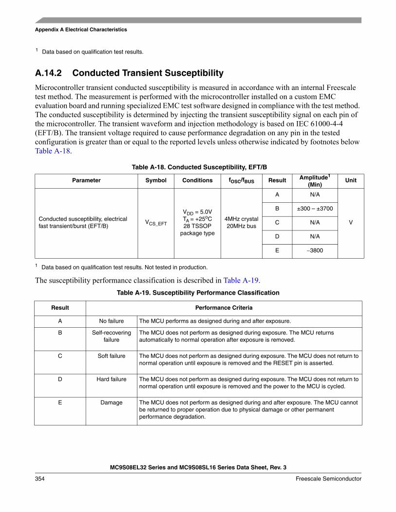
Appendix A Electrical Characteristics
MC9S08EL32 Series and MC9S08SL16 Series Data Sheet, Rev. 3
354 Freescale Semiconductor
A.14.2 Conducted Transient Susceptibility
Microcontroller transient conducted susceptibility is measured in accordance with an internal Freescale test method. The measurement is performed with the microcontroller installed on a custom EMC evaluation board and running specialized EMC test software designed in compliance with the test method. The conducted susceptibility is determined by injecting the transient susceptibility signal on each pin of the microcontroller. The transient waveform and injection methodology is based on IEC 61000-4-4 (EFT/B). The transient voltage required to cause performance degradation on any pin in the tested configuration is greater than or equal to the reported levels unless otherwise indicated by footnotes below Table A-18.
The susceptibility performance classification is described in Table A-19.
1 Data based on qualification test results.
Table A-18. Conducted Susceptibility, EFT/B
Parameter Symbol Conditions fOSC/fBUS Result Amplitude1
(Min)
1 Data based on qualification test results. Not tested in production.
Unit
Conducted susceptibility, electrical fast transient/burst (EFT/B)
VCS_EFT
VDD = 5.0VTA = +25oC28 TSSOP
package type
4MHz crystal20MHz bus
A N/A
V
B ±300 – ±3700
C N/A
D N/A
E −3800
Table A-19. Susceptibility Performance Classification
Result Performance Criteria
A No failure The MCU performs as designed during and after exposure.
B Self-recovering failure
The MCU does not perform as designed during exposure. The MCU returns automatically to normal operation after exposure is removed.
C Soft failure The MCU does not perform as designed during exposure. The MCU does not return to normal operation until exposure is removed and the RESET pin is asserted.
D Hard failure The MCU does not perform as designed during exposure. The MCU does not return to normal operation until exposure is removed and the power to the MCU is cycled.
E Damage The MCU does not perform as designed during and after exposure. The MCU cannot be returned to proper operation due to physical damage or other permanent performance degradation.
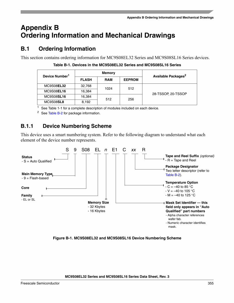
Appendix B Ordering Information and Mechanical Drawings
MC9S08EL32 Series and MC9S08SL16 Series Data Sheet, Rev. 3
Freescale Semiconductor 355
Appendix BOrdering Information and Mechanical Drawings
B.1 Ordering InformationThis section contains ordering information for MC9S08EL32 Series and MC9S08SL16 Series devices.
B.1.1 Device Numbering Scheme
This device uses a smart numbering system. Refer to the following diagram to understand what each element of the device number represents.
Figure B-1. MC9S08EL32 and MC9S08SL16 Device Numbering Scheme
Table B-1. Devices in the MC9S08EL32 Series and MC9S08SL16 Series
Device Number1
1 See Table 1-1 for a complete description of modules included on each device.
MemoryAvailable Packages2
2 See Table B-2 for package information.
FLASH RAM EEPROM
MC9S08EL32 32,7681024 512
28-TSSOP, 20-TSSOPMC9S08EL16 16,384
MC9S08SL16 16,384512 256
MC9S08SL8 8,192
S 9 S08 EL n E1 C xx R
Status- S = Auto Qualified
Main Memory Type- 9 = Flash-based
Core
Family- EL or SL
Memory Size- 32 Kbytes- 16 Kbytes
Mask Set Identifier — this field only appears in “Auto Qualified” part numbers- Alpha character references
wafer fab.- Numeric character identifies
mask.
Temperature Option- C = –40 to 85 °C- V = –40 to 105 °C- M = –40 to 125 °C
Package DesignatorTwo letter descriptor (refer to Table B-2).
Tape and Reel Suffix (optional)- R = Tape and Reel
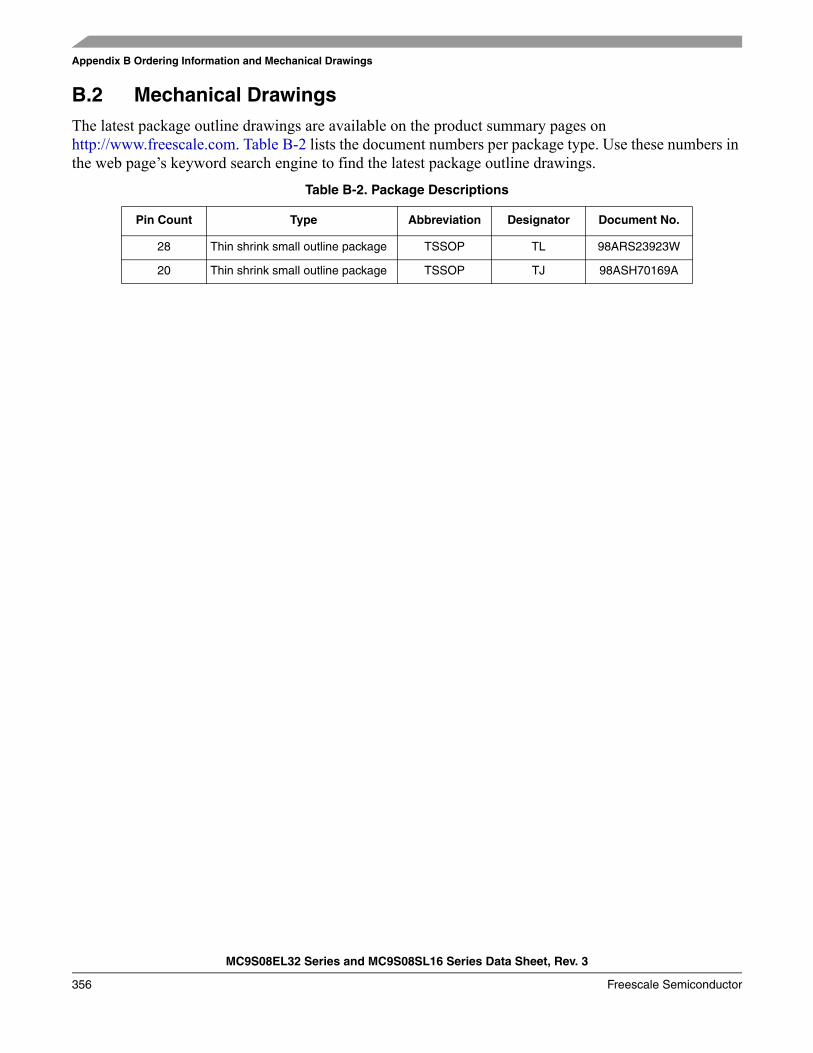
Appendix B Ordering Information and Mechanical Drawings
MC9S08EL32 Series and MC9S08SL16 Series Data Sheet, Rev. 3
356 Freescale Semiconductor
B.2 Mechanical DrawingsThe latest package outline drawings are available on the product summary pages on http://www.freescale.com. Table B-2 lists the document numbers per package type. Use these numbers in the web page’s keyword search engine to find the latest package outline drawings.
Table B-2. Package Descriptions
Pin Count Type Abbreviation Designator Document No.
28 Thin shrink small outline package TSSOP TL 98ARS23923W
20 Thin shrink small outline package TSSOP TJ 98ASH70169A

MC9S08EL32Rev. 3, 7/2008
How to Reach Us:
Home Page:www.freescale.com
E-mail:[email protected]
USA/Europe or Locations Not Listed:Freescale SemiconductorTechnical Information Center, CH3701300 N. Alma School RoadChandler, Arizona 85224+1-800-521-6274 or [email protected]
Europe, Middle East, and Africa:Freescale Halbleiter Deutschland GmbHTechnical Information CenterSchatzbogen 781829 Muenchen, Germany+44 1296 380 456 (English)+46 8 52200080 (English)+49 89 92103 559 (German)+33 1 69 35 48 48 (French)[email protected]
Japan:Freescale Semiconductor Japan Ltd.HeadquartersARCO Tower 15F1-8-1, Shimo-Meguro, Meguro-ku,Tokyo 153-0064Japan0120 191014 or +81 3 5437 [email protected]
Asia/Pacific:Freescale Semiconductor China Ltd.Exchange Building 23FNo. 118 Jianguo RoadChaoyang DistrictBeijing 100022China+86 10 5879 [email protected]
For Literature Requests Only:Freescale Semiconductor Literature Distribution CenterP.O. Box 5405Denver, Colorado 802171-800-441-2447 or 1-303-675-2140Fax: [email protected]
Information in this document is provided solely to enable system and software implementers to use Freescale Semiconductor products. There are no express or implied copyright licenses granted hereunder to design or fabricate any integrated circuits or integrated circuits based on the information in this document.
Freescale Semiconductor reserves the right to make changes without further notice to any products herein. Freescale Semiconductor makes no warranty, representation or guarantee regarding the suitability of its products for any particular purpose, nor does Freescale Semiconductor assume any liability arising out of the application or use of any product or circuit, and specifically disclaims any and all liability, including without limitation consequential or incidental damages. “Typical” parameters that may be provided in Freescale Semiconductor data sheets and/or specifications can and do vary in different applications and actual performance may vary over time. All operating parameters, including “Typicals”, must be validated for each customer application by customer’s technical experts. Freescale Semiconductor does not convey any license under its patent rights nor the rights of others. Freescale Semiconductor products are not designed, intended, or authorized for use as components in systems intended for surgical implant into the body, or other applications intended to support or sustain life, or for any other application in which the failure of the Freescale Semiconductor product could create a situation where personal injury or death may occur. Should Buyer purchase or use Freescale Semiconductor products for any such unintended or unauthorized application, Buyer shall indemnify and hold Freescale Semiconductor and its officers, employees, subsidiaries, affiliates, and distributors harmless against all claims, costs, damages, and expenses, and reasonable attorney fees arising out of, directly or indirectly, any claim of personal injury or death associated with such unintended or unauthorized use, even if such claim alleges that Freescale Semiconductor was negligent regarding the design or manufacture of the part.
Freescale™ and the Freescale logo are trademarks of Freescale Semiconductor, Inc.All other product or service names are the property of their respective owners.
© Freescale Semiconductor, Inc. 2008. All rights reserved.