datasheet irfb
8
IRFB20N50K 4/2/02 www.irf.com 1 SMPS MOSFET HEXFET ® Power MOSFET V DSS R DS(on) typ. I D 500V 0.21Ω 20A Parameter Max. Units I D @ T C = 25°C Continuous Drain Current, V GS @ 10V 20 I D @ T C = 100°C Continuous Drain Current, V GS @ 10V 12 A I DM Pulsed Drain Current 80 P D @T C = 25°C Power Dissipation 280 W Linear Derating Factor 2.2 W/°C V GS Gate-to-Source Voltage ± 30 V dv/dt Peak Diode Recovery dv/dt 6.9 V/ns T J Operating Junction and -55 to + 150 T STG Storage Temperature Range Soldering Temperature, for 10 seconds 300 (1.6mm from case ) °C Mounting Torque, 6-32 or M3 screw 10 N Absolute Maximum Ratings TO- 220AB l Switch Mode Power Supply (SMPS) l Uninterruptible Power Supply l High Speed Power Switching l Hard Switched and High Frequency Circuits Benefits Applications l Low Gate Charge Qg results in Simple Drive Requirement l Improved Gate, Avalanche and Dynamicdv/dt Ruggedness l Fully Characterized Capacitance and Avalanche Voltage and Current l Low R DS(on) Symbol Parameter Typ. Max. Units E AS Single Pulse Avalanche Energy ––– 330 mJ I AR Avalanche Current ––– 20 A E AR Repetitive Avalanche Energy ––– 28 mJ Avalanche Characteristics Symbol Parameter Typ. Max. Units R θJC Junction-to-Case ––– 0.45 R θCS Case-to-Sink, Flat, Greased Surface 0.50 ––– °C/W R θJA Junction-to-Ambient ––– 58 Thermal Resistance PD - 94418
-
Upload
farides-pitre -
Category
Documents
-
view
212 -
download
0
Transcript of datasheet irfb

IRFB20N50K
4/2/02
www.irf.com 1
SMPS MOSFETHEXFETPower MOSFET
VDSS RDS(on) typ. ID500V 0.21Ω 20A
Parameter Max. UnitsID @ TC = 25°C Continuous Drain Current, VGS @ 10V 20ID @ TC = 100°C Continuous Drain Current, VGS @ 10V 12 AIDM Pulsed Drain Current 80PD @TC = 25°C Power Dissipation 280 W
Linear Derating Factor 2.2 W/°CVGS Gate-to-Source Voltage ± 30 Vdv/dt Peak Diode Recovery dv/dt 6.9 V/nsTJ Operating Junction and -55 to + 150TSTG Storage Temperature Range
Soldering Temperature, for 10 seconds 300 (1.6mm from case )
°C
Mounting Torque, 6-32 or M3 screw 10 N
Absolute Maximum Ratings
TO-220AB
Switch Mode Power Supply (SMPS) Uninterruptible Power Supply High Speed Power Switching Hard Switched and High Frequency Circuits
Benefits
Applications
Low Gate Charge Qg results in Simple Drive Requirement Improved Gate, Avalanche and Dynamicdv/dt Ruggedness Fully Characterized Capacitance and Avalanche Voltage
and Current Low RDS(on)
Symbol Parameter Typ. Max. UnitsEAS Single Pulse Avalanche Energy ––– 330 mJIAR Avalanche Current ––– 20 AEAR Repetitive Avalanche Energy ––– 28 mJ
Avalanche Characteristics
Symbol Parameter Typ. Max. UnitsRθJC Junction-to-Case ––– 0.45RθCS Case-to-Sink, Flat, Greased Surface 0.50 ––– °C/WRθJA Junction-to-Ambient ––– 58
Thermal Resistance
PD - 94418
2 www.irf.com
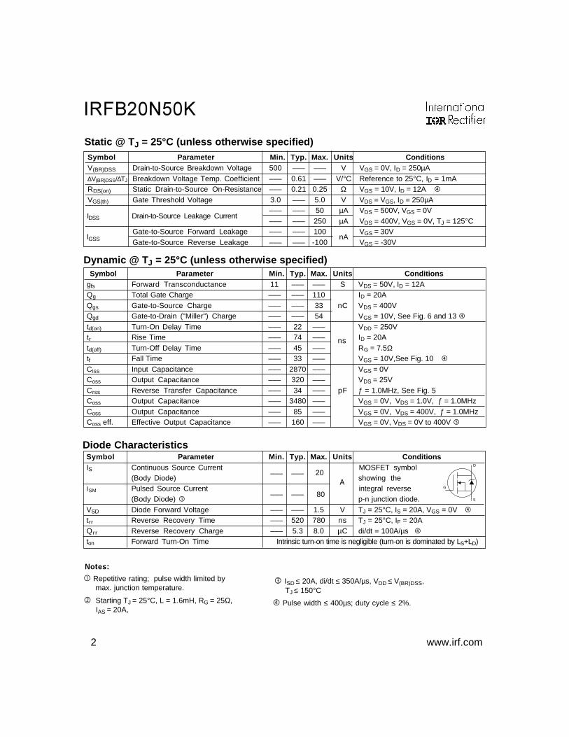
Dynamic @ TJ = 25°C (unless otherwise specified)
Symbol Parameter Min. Typ. Max. Units ConditionsV(BR)DSS Drain-to-Source Breakdown Voltage 500 ––– ––– V VGS = 0V, ID = 250µA∆V(BR)DSS/∆TJ Breakdown Voltage Temp. Coefficient ––– 0.61 ––– V/°C Reference to 25°C, ID = 1mARDS(on) Static Drain-to-Source On-Resistance ––– 0.21 0.25 Ω VGS = 10V, ID = 12AVGS(th) Gate Threshold Voltage 3.0 ––– 5.0 V VDS = VGS, ID = 250µA
––– ––– 50 µA VDS = 500V, VGS = 0V––– ––– 250 µA VDS = 400V, VGS = 0V, TJ = 125°C
Gate-to-Source Forward Leakage ––– ––– 100 VGS = 30VGate-to-Source Reverse Leakage ––– ––– -100
nAVGS = -30V
Static @ TJ = 25°C (unless otherwise specified)
IGSS
IDSS Drain-to-Source Leakage Current
Repetitive rating; pulse width limited by max. junction temperature.
ISD ≤ 20A, di/dt ≤ 350A/µs, VDD ≤ V(BR)DSS, TJ ≤ 150°C
Starting TJ = 25°C, L = 1.6mH, RG = 25Ω, IAS = 20A,
Pulse width ≤ 400µs; duty cycle ≤ 2%.
Symbol Parameter Min. Typ. Max. Units Conditionsgfs Forward Transconductance 11 ––– ––– S VDS = 50V, ID = 12AQg Total Gate Charge ––– ––– 110 ID = 20AQgs Gate-to-Source Charge ––– ––– 33 nC VDS = 400VQgd Gate-to-Drain ("Miller") Charge ––– ––– 54 VGS = 10V, See Fig. 6 and 13 td(on) Turn-On Delay Time ––– 22 ––– VDD = 250Vtr Rise Time ––– 74 ––– ID = 20Atd(off) Turn-Off Delay Time ––– 45 ––– RG = 7.5Ωtf Fall Time ––– 33 ––– VGS = 10V,See Fig. 10Ciss Input Capacitance ––– 2870 ––– VGS = 0VCoss Output Capacitance ––– 320 ––– VDS = 25VCrss Reverse Transfer Capacitance ––– 34 ––– pF ƒ = 1.0MHz, See Fig. 5Coss Output Capacitance ––– 3480 ––– VGS = 0V, VDS = 1.0V, ƒ = 1.0MHzCoss Output Capacitance ––– 85 ––– VGS = 0V, VDS = 400V, ƒ = 1.0MHzCoss eff. Effective Output Capacitance ––– 160 ––– VGS = 0V, VDS = 0V to 400V
ns
Symbol Parameter Min. Typ. Max. Units ConditionsIS Continuous Source Current MOSFET symbol
(Body Diode)––– –––
showing theISM Pulsed Source Current integral reverse
(Body Diode) ––– –––
p-n junction diode.VSD Diode Forward Voltage ––– ––– 1.5 V TJ = 25°C, IS = 20A, VGS = 0Vtrr Reverse Recovery Time ––– 520 780 ns TJ = 25°C, IF = 20AQrr Reverse Recovery Charge ––– 5.3 8.0 µC di/dt = 100A/µston Forward Turn-On Time Intrinsic turn-on time is negligible (turn-on is dominated by LS+LD)
S
D
G
Diode Characteristics
20
80
www.irf.com 3
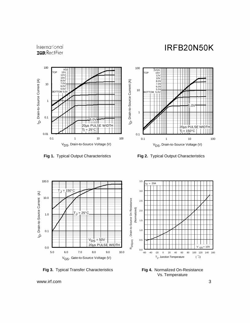
Fig 4. Normalized On-ResistanceVs. Temperature
Fig 2. Typical Output CharacteristicsFig 1. Typical Output Characteristics
Fig 3. Typical Transfer Characteristics
0.1 1 10 100
VDS, Drain-to-Source Voltage (V)
0.01
0.1
1
10
100
I D, D
rain
-to-
Sou
rce
Cur
rent
(A
)
5.0V
20µs PULSE WIDTHTj = 25°C
VGSTOP 15V 12V 10V 8.0V 7.0V 6.0V 5.5VBOTTOM 5.0V
5.0 6.0 7.0 8.0 9.0 10.0
VGS, Gate-to-Source Voltage (V)
0.0
0.1
1.0
10.0
100.0
I D, D
rain
-to-
Sou
rce
Cur
rent
(Α
)
TJ = 25°C
TJ = 150°C
VDS = 50V
20µs PULSE WIDTH
0.1 1 10 100
VDS, Drain-to-Source Voltage (V)
0.1
1
10
100
I D, D
rain
-to-
Sou
rce
Cur
rent
(A
)
5.0V
20µs PULSE WIDTHTj = 150°C
VGSTOP 15V 12V 10V 8.0V 7.0V 6.0V 5.5VBOTTOM 5.0V
-60 -40 -20 0 20 40 60 80 100 120 140 1600.0
0.5
1.0
1.5
2.0
2.5
3.0
3.5
T , Junction Temperature ( C)
R
, D
rain
-to-
Sou
rce
On
Res
ista
nce
(Nor
mal
ized
)
J
DS
(on)
°
V =
I =
GS
D
10V
20A

4 www.irf.com
Fig 8. Maximum Safe Operating Area
Fig 6. Typical Gate Charge Vs.Gate-to-Source Voltage
Fig 5. Typical Capacitance Vs.Drain-to-Source Voltage
Fig 7. Typical Source-Drain DiodeForward Voltage
1 10 100 1000
VDS, Drain-to-Source Voltage (V)
10
100
1000
10000
100000
C, C
apac
itanc
e (p
F)
Coss
Crss
Ciss
VGS = 0V, f = 1 MHZCiss = C gs + C gd , C ds SHORTED
Crss = Cgd Coss = Cds + Cgd
1 10 100 1000 10000
VDS , Drain-toSource Voltage (V)
0.1
1
10
100
1000
I D,
Dra
in-t
o-S
ourc
e C
urre
nt (
A)
Tc = 25°CTj = 150°CSingle Pulse
1msec
10msec
OPERATION IN THIS AREA LIMITED BY RDS(on)
100µsec
0.2 0.4 0.6 0.8 1.0 1.2
VSD, Source-toDrain Voltage (V)
0.1
1.0
10.0
100.0
I SD
, Rev
erse
Dra
in C
urre
nt (A
)
TJ = 25°C
TJ = 150°C
VGS = 0V
0 20 40 60 80 100 1200
4
8
12
16
20
Q , Total Gate Charge (nC)
V
, G
ate-
to-S
ourc
e V
olta
ge (
V)
G
GS
FOR TEST CIRCUITSEE FIGURE
I =D
13
21A
V = 100VDS
V = 250VDS
V = 400VDS

www.irf.com 5
Fig 10a. Switching Time Test Circuit
VDS
90%
10%VGS
td(on) tr td(off) tf
Fig 10b. Switching Time Waveforms
≤ 1 ≤ 0.1 %
+-
Fig 11. Maximum Effective Transient Thermal Impedance, Junction-to-Case
Fig 9. Maximum Drain Current Vs.Case Temperature
0.001
0.01
0.1
1
0.00001 0.0001 0.001 0.01 0.1 1
Notes:
1. Duty factor D = t / t
2. Peak T = P x Z + T
1 2
J DM thJC C
P
t
t
DM
1
2
t , Rectangular Pulse Duration (sec)
The
rmal
Res
pons
e(Z
)
1
thJC
0.010.02
0.05
0.10
0.20
D = 0.50
SINGLE PULSE(THERMAL RESPONSE)
25 50 75 100 125 1500
4
8
12
16
20
I ,
Dra
in C
urre
nt (
A)
D

6 www.irf.com
QG
QGS QGD
VG
Charge
D.U.T.VDS
IDIG
3mA
VGS
.3µF
50KΩ
.2µF12V
Current RegulatorSame Type as D.U.T.
Current Sampling Resistors
+
-
Fig 13b. Gate Charge Test CircuitFig 13a. Basic Gate Charge Waveform
Fig 12b. Unclamped Inductive Waveforms
Fig 12a. Unclamped Inductive Test Circuit
tp
V(BR)DSS
IAS
Fig 12c. Maximum Avalanche EnergyVs. Drain Current
RG
IAS
0.01Ωtp
D.U.T
LVDS
+- VDD
DRIVER
A
15V
20VVGS
25 50 75 100 125 1500
100
200
300
400
500
600
E
, S
ingl
e P
ulse
Ava
lanc
he E
nerg
y (m
J)A
S
IDTOP
BOTTOM
9.4A
17A
20A
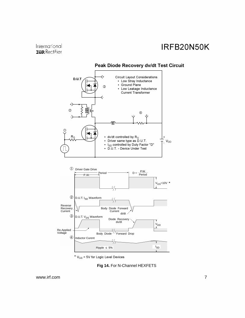
www.irf.com 7
P.W.Period
di/dt
Diode Recoverydv/dt
Ripple ≤ 5%
Body Diode Forward DropRe-AppliedVoltage
ReverseRecoveryCurrent
Body Diode ForwardCurrent
VGS=10V
VDD
ISD
Driver Gate Drive
D.U.T. ISD Waveform
D.U.T. VDS Waveform
Inductor Curent
D = P.W.Period
+
-
+
+
+-
-
-
Fig 14. For N-Channel HEXFETS
• • !" • #$ %%• &
'# #' • () # • *#+ • ( , # '# !

8 www.irf.com
LEAD ASSIGNMENTS 1 - GATE 2 - DRAIN 3 - SOURCE 4 - DRAIN
- B -
1.32 (.052)1.22 (.048)
3X0.55 (.022)0.46 (.018)
2.92 (.115)2.64 (.104)
4.69 (.185)4.20 (.165)
3X0.93 (.037)0.69 (.027)
4.06 (.160)3.55 (.140)
1.15 (.045) MIN
6.47 (.255)6.10 (.240)
3.78 (.149)3.54 (.139)
- A -
10.54 (.415)10.29 (.405)2.87 (.113)
2.62 (.103)
15.24 (.600)14.84 (.584)
14.09 (.555)13.47 (.530)
3X1.40 (.055)1.15 (.045)
2.54 (.100)
2X
0.36 (.014) M B A M
4
1 2 3
NOTES:
1 DIMENSIONING & TOLERANCING PER ANSI Y14.5M, 1982. 3 OUTLINE CONFORMS TO JEDEC OUTLINE TO-220AB.
2 CONTROLLING DIMENSION : INCH 4 HEATSINK & LEAD MEASUREMENTS DO NOT INCLUDE BURRS.
TO-220 Part Marking Information
TO-220 Package OutlineDimensions are shown in millimeters (inches)
EXAMPLE: THIS IS AN IRF1010
LOT CODE 1789ASSEMBLED ON WW 19, 1997IN THE ASSEMBLY LINE "C"
INTERNAT IONALRECT IFIER
LOGO
ASSEMBLYLOT CODE
PART NUMBER
DATE CODEYEAR 7 = 1997WEEK 19LINE C
Data and specifications subject to change without notice. This product has been designed and qualified for the Industrial market.
Qualification Standards can be found on IR’s Web site.
IR WORLD HEADQUARTERS: 233 Kansas St., El Segundo, California 90245, USA Tel: (310) 252-7105TAC Fax: (310) 252-7903
Visit us at www.irf.com for sales contact information.4/02