Talent Acquisition and Recruitment Services Performance Development
4/10/2013
1
Data acquisition and instrumentation
START Lecture
Sam Sadeghi
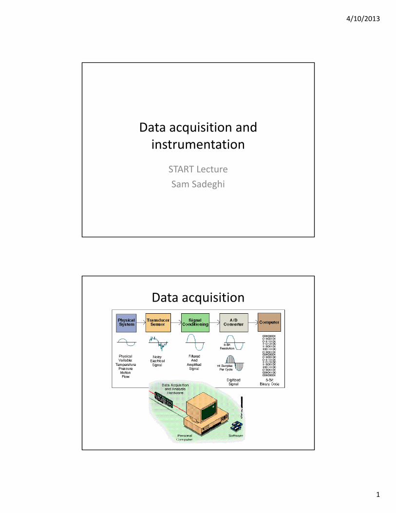
Data acquisition
4/10/2013
2
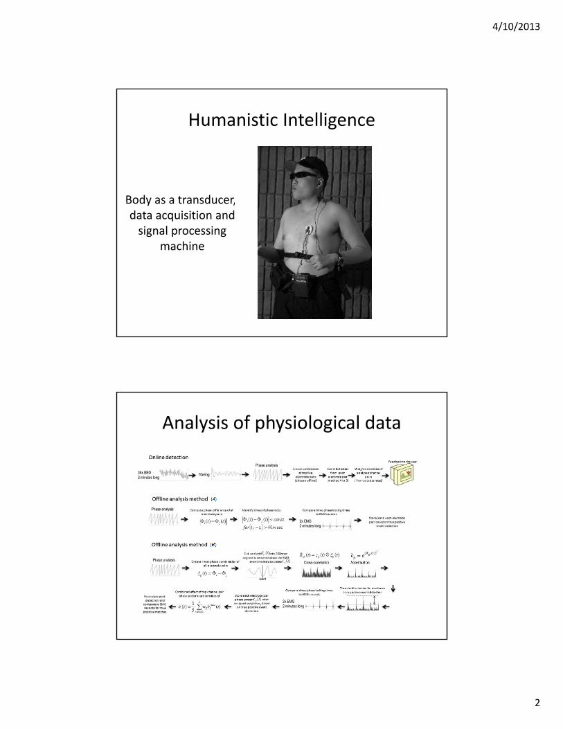
Body as a transducer,, data acquisition and signal processing
machine
Humanistic Intelligence
Analysis of physiological data
4/10/2013
3
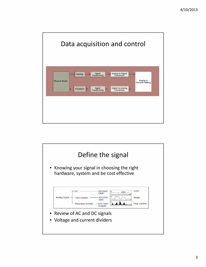
Data acquisition and control
Define the signal
• Knowing your signal in choosing the right hardware, system and be cost effective
• Review of AC and DC signals
• Voltage and current dividers
4/10/2013
4
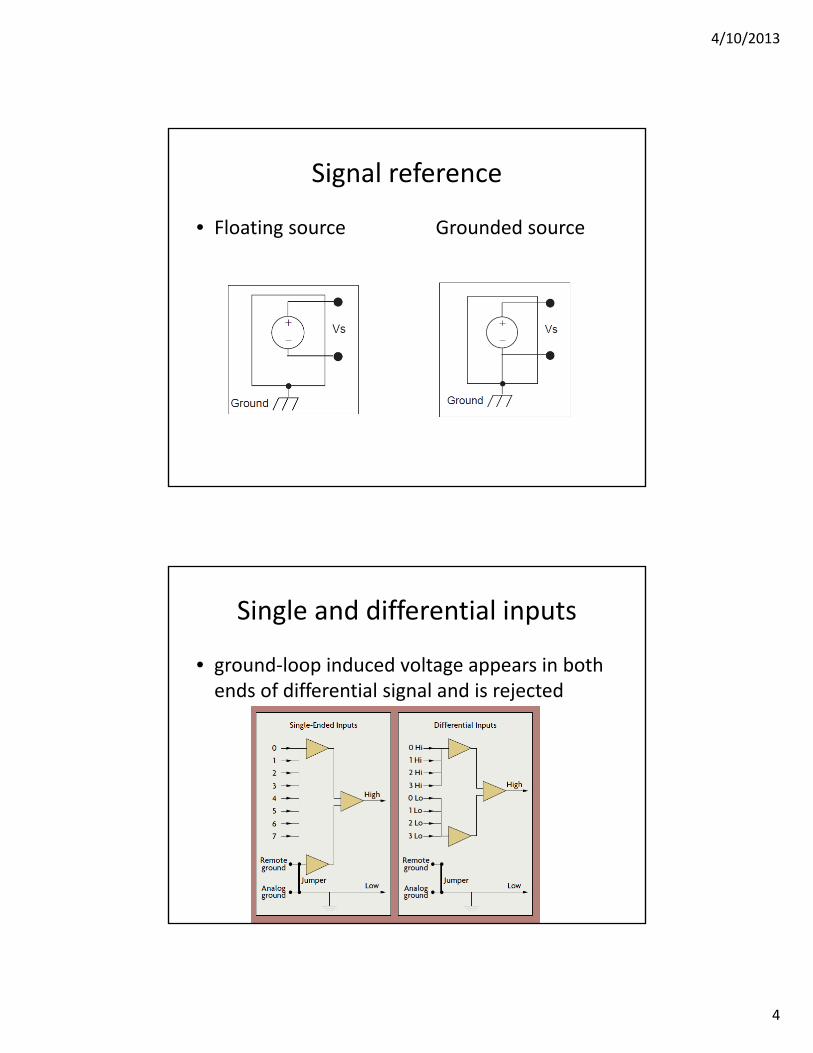
Signal reference
• Floating source Grounded source
Single and differential inputs
• ground‐loop induced voltage appears in both ends of differential signal and is rejected
4/10/2013
5
Signal conditioning
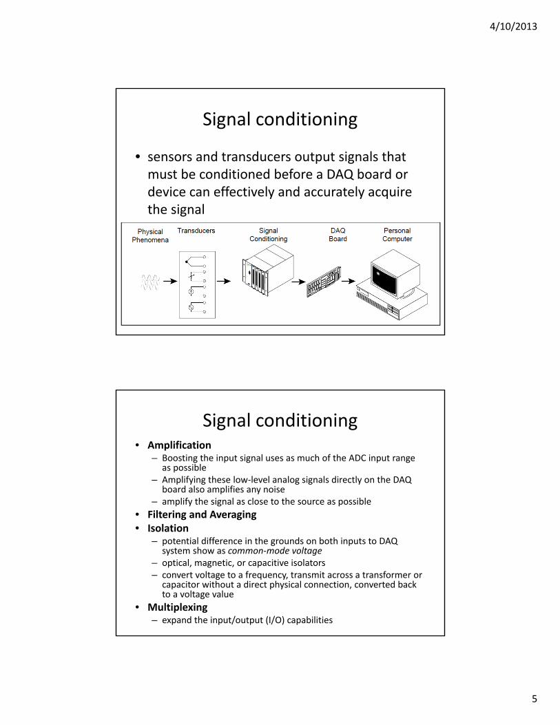
• sensors and transducers output signals that must be conditioned before a DAQ board or device can effectively and accurately acquire the signal
Signal conditioning• Amplification
– Boosting the input signal uses as much of the ADC input range as possible
– Amplifying these low‐level analog signals directly on the DAQ board also amplifies any noise
– amplify the signal as close to the source as possible
• Filtering and Averaging• Isolation
– potential difference in the grounds on both inputs to DAQ system show as common‐mode voltage
– optical, magnetic, or capacitive isolators– convert voltage to a frequency, transmit across a transformer or
capacitor without a direct physical connection, converted back to a voltage value
• Multiplexing– expand the input/output (I/O) capabilities
4/10/2013
6
Amplification
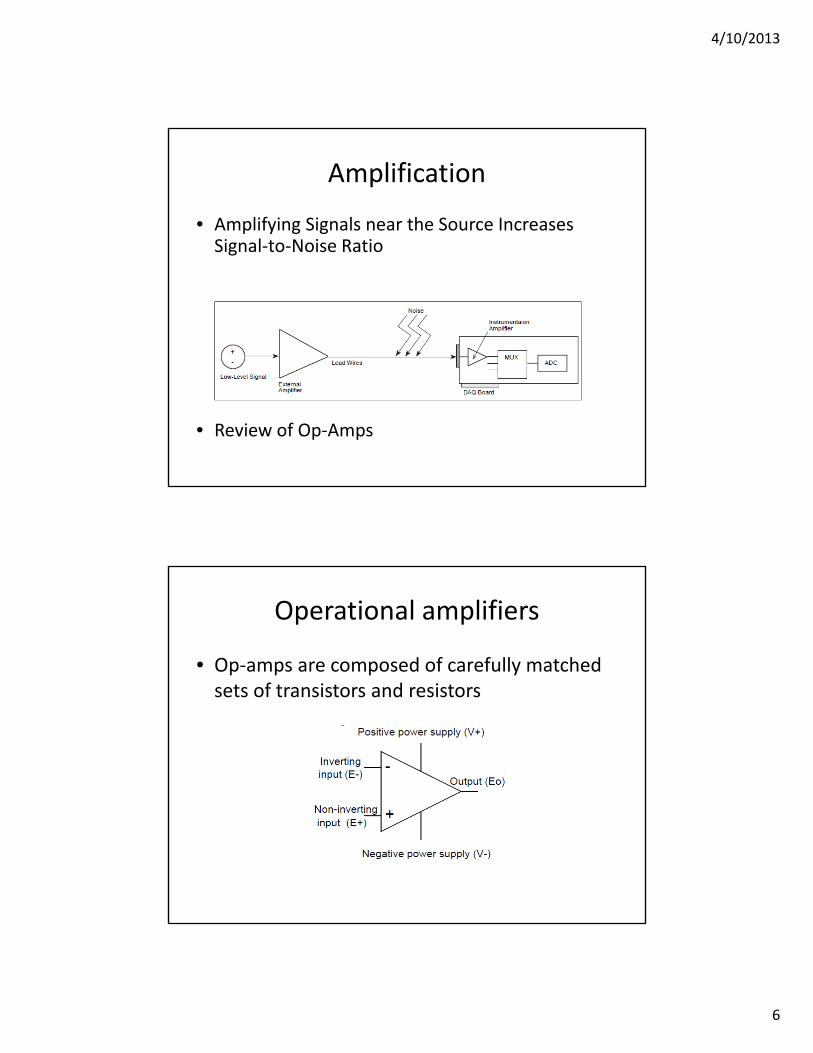
• Amplifying Signals near the Source Increases Signal‐to‐Noise Ratio
• Review of Op‐Amps
Operational amplifiers
• Op‐amps are composed of carefully matched sets of transistors and resistors
4/10/2013
7
Op‐amps
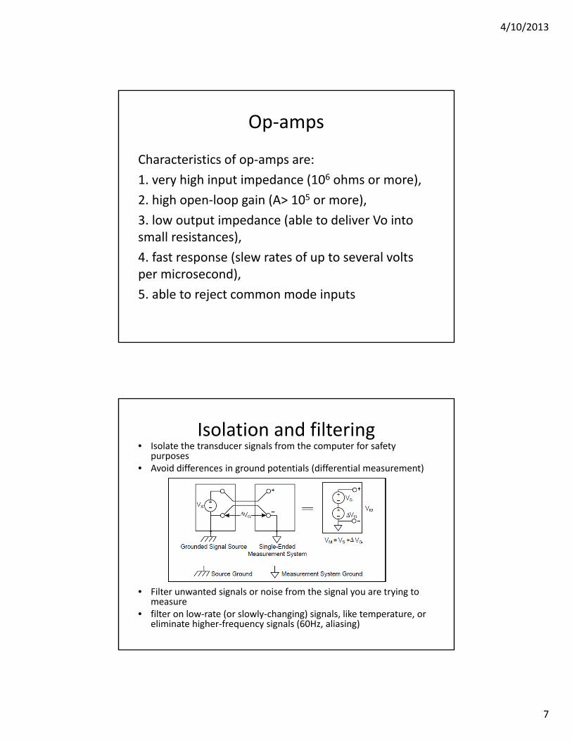
Characteristics of op‐amps are:
1. very high input impedance (106 ohms or more),
2. high open‐loop gain (A> 105 or more),
3. low output impedance (able to deliver Vo into small resistances),
4. fast response (slew rates of up to several volts per microsecond),
5. able to reject common mode inputs
Isolation and filtering• Isolate the transducer signals from the computer for safety
purposes• Avoid differences in ground potentials (differential measurement)
• Filter unwanted signals or noise from the signal you are trying to measure
• filter on low‐rate (or slowly‐changing) signals, like temperature, or eliminate higher‐frequency signals (60Hz, aliasing)
4/10/2013
8
Sampling
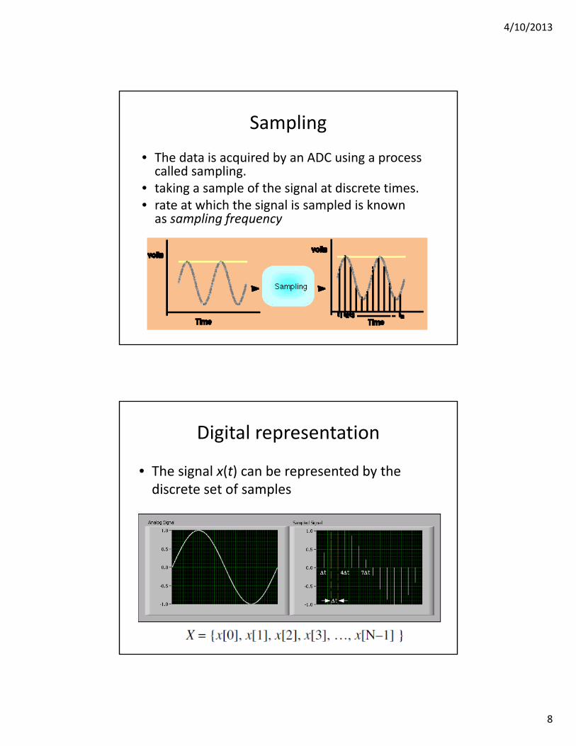
• The data is acquired by an ADC using a process called sampling.
• taking a sample of the signal at discrete times. • rate at which the signal is sampled is known as sampling frequency
Digital representation
• The signal x(t) can be represented by the discrete set of samples
4/10/2013
9
Sampling rate
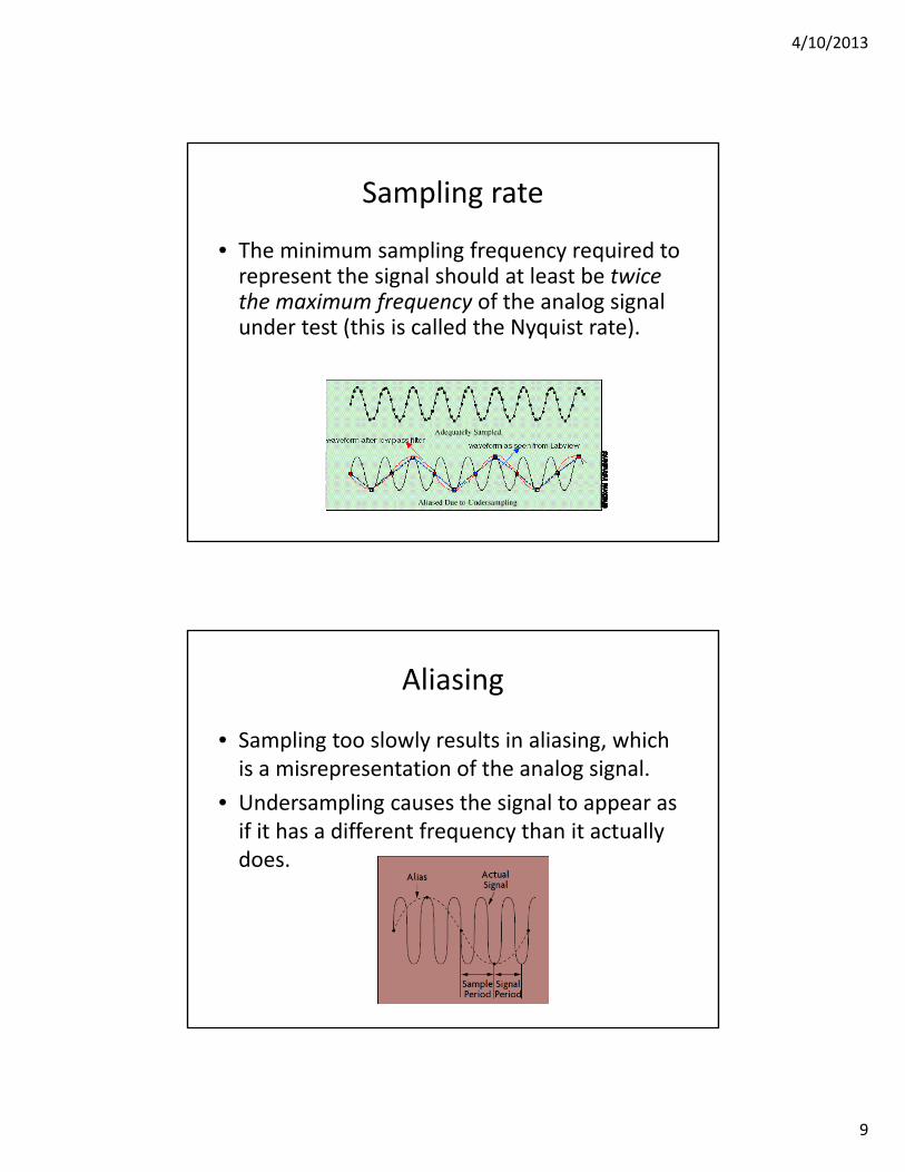
• The minimum sampling frequency required to represent the signal should at least be twice the maximum frequency of the analog signal under test (this is called the Nyquist rate).
Aliasing
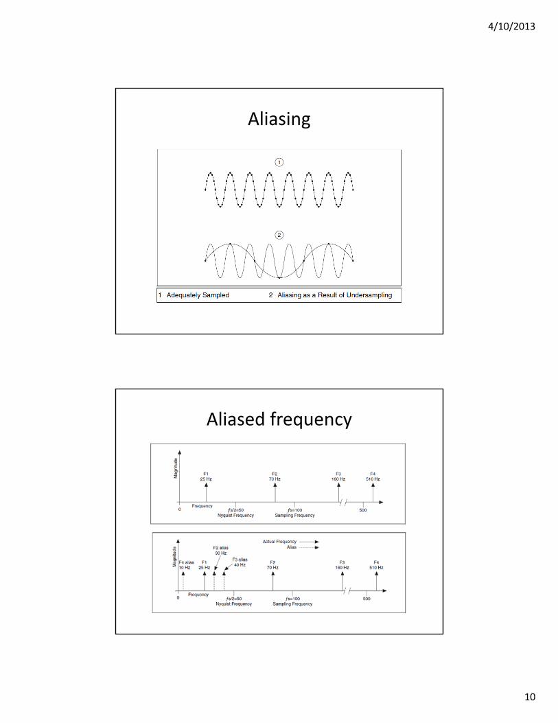
• Sampling too slowly results in aliasing, which is a misrepresentation of the analog signal.
• Undersampling causes the signal to appear as if it has a different frequency than it actually does.
4/10/2013
10
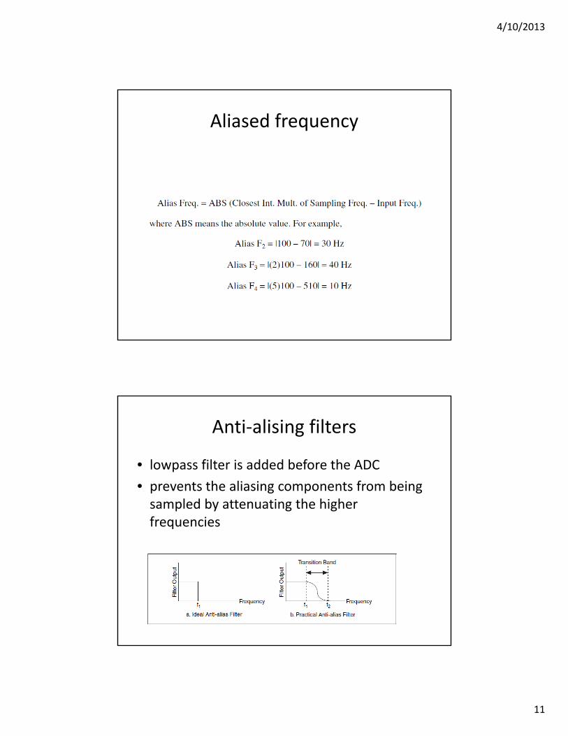
Aliasing
Aliased frequency
4/10/2013
11
Aliased frequency
Anti‐alising filters
• lowpass filter is added before the ADC
• prevents the aliasing components from being sampled by attenuating the higher frequencies
4/10/2013
12
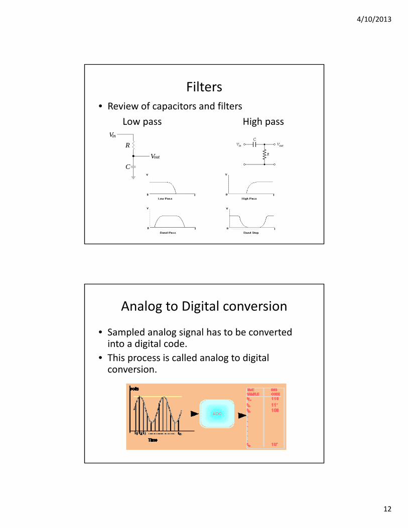
Filters• Review of capacitors and filters
Low pass High pass
Analog to Digital conversion
• Sampled analog signal has to be converted into a digital code.
• This process is called analog to digital conversion.
4/10/2013
13
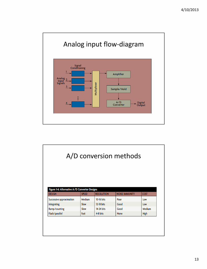
Analog input flow‐diagram
A/D conversion methods
4/10/2013
14
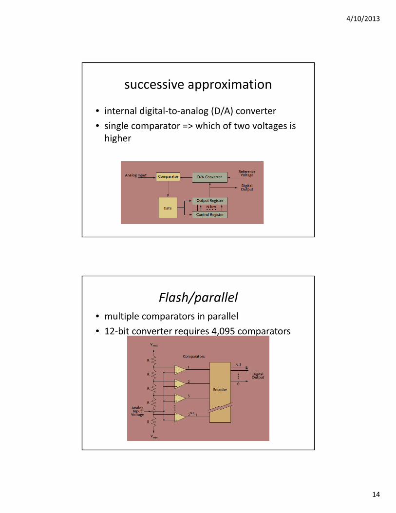
successive approximation
• internal digital‐to‐analog (D/A) converter
• single comparator => which of two voltages is higher
Flash/parallel• multiple comparators in parallel
• 12‐bit converter requires 4,095 comparators
4/10/2013
15
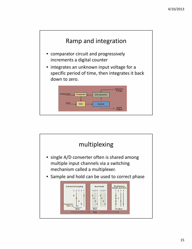
Ramp and integration
• comparator circuit and progressively increments a digital counter
• integrates an unknown input voltage for a specific period of time, then integrates it back down to zero.
multiplexing
• single A/D converter often is shared among multiple input channels via a switching mechanism called a multiplexer.
• Sample and hold can be used to correct phase
4/10/2013
16
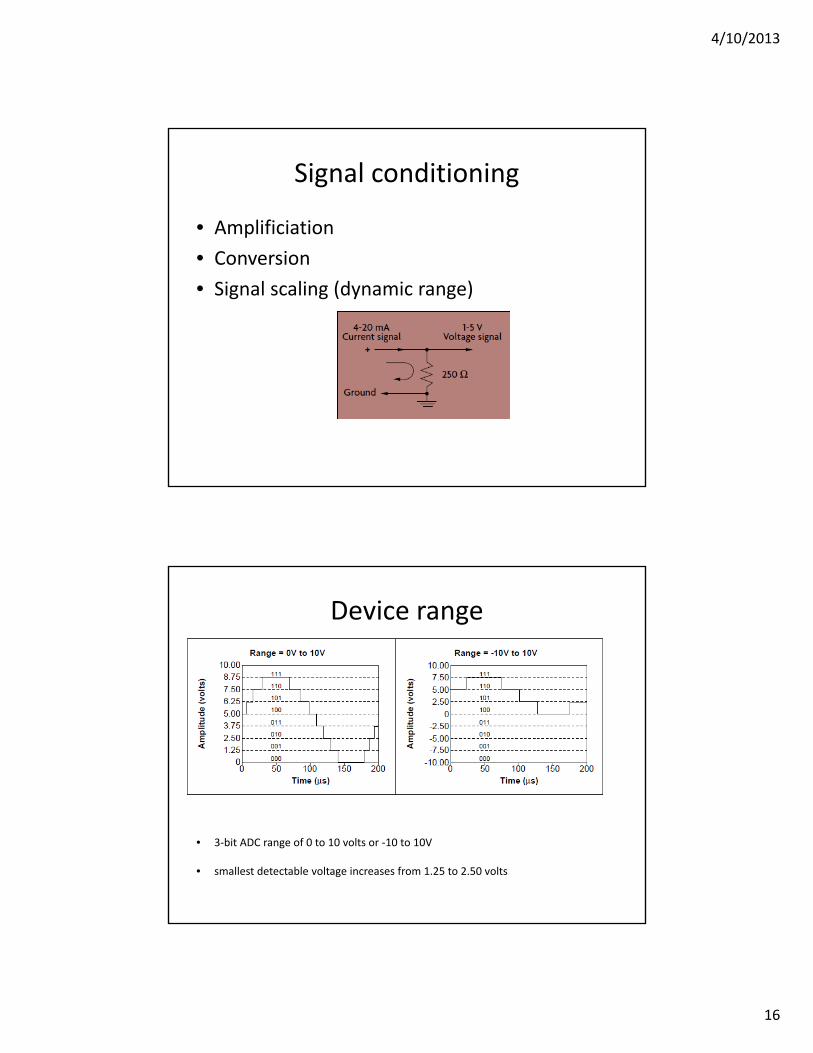
Signal conditioning
• Amplificiation
• Conversion
• Signal scaling (dynamic range)
Device range
• 3‐bit ADC range of 0 to 10 volts or ‐10 to 10V
• smallest detectable voltage increases from 1.25 to 2.50 volts
4/10/2013
17
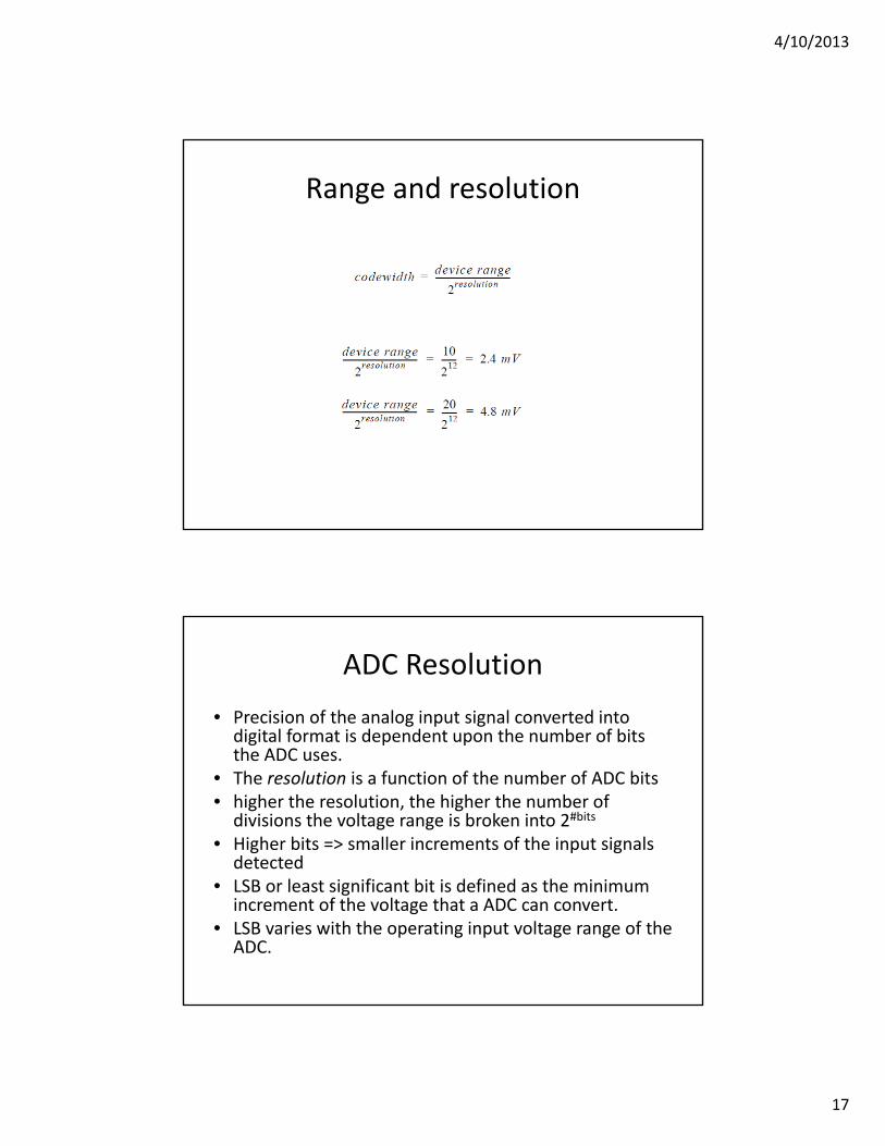
Range and resolution
ADC Resolution
• Precision of the analog input signal converted into digital format is dependent upon the number of bits the ADC uses.
• The resolution is a function of the number of ADC bits• higher the resolution, the higher the number of divisions the voltage range is broken into 2#bits
• Higher bits => smaller increments of the input signals detected
• LSB or least significant bit is defined as the minimum increment of the voltage that a ADC can convert.
• LSB varies with the operating input voltage range of the ADC.
4/10/2013
18
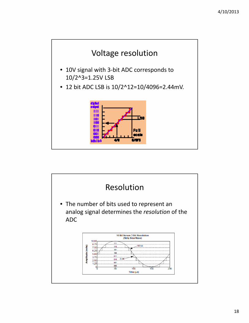
Voltage resolution
• 10V signal with 3‐bit ADC corresponds to 10/2^3=1.25V LSB
• 12 bit ADC LSB is 10/2^12=10/4096=2.44mV.
Resolution
• The number of bits used to represent an analog signal determines the resolution of the ADC
4/10/2013
19
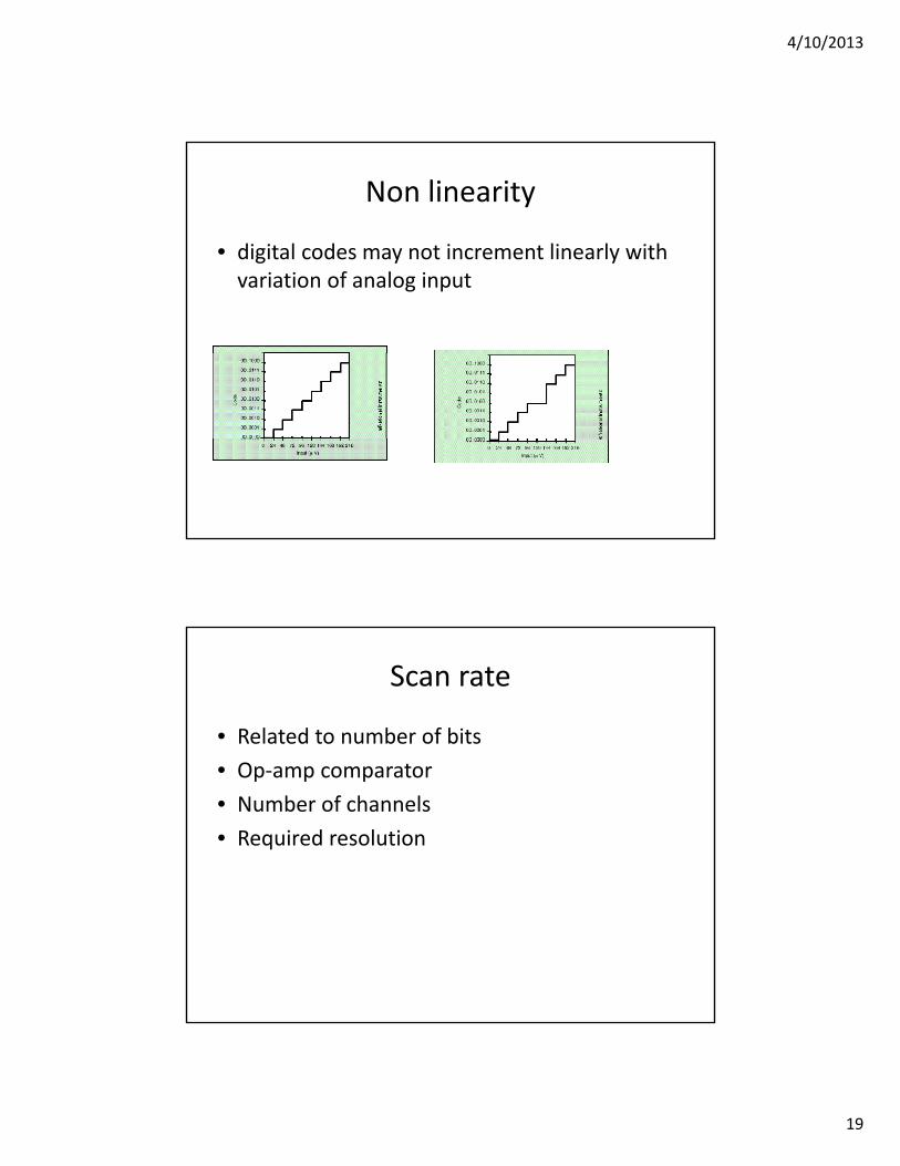
Non linearity
• digital codes may not increment linearly with variation of analog input
Scan rate
• Related to number of bits
• Op‐amp comparator
• Number of channels
• Required resolution
4/10/2013
20
Settling time
• Analog signal is:– selected by a multiplexer– Amplified– converted by the ADC.
• The amplifier must be in sync with multiplexer and ADC
• If wait time is insufficient ADC can convert the signal that is still in transition from the previous value
• settling time changes with sampling rate and the gain of the DAQ board
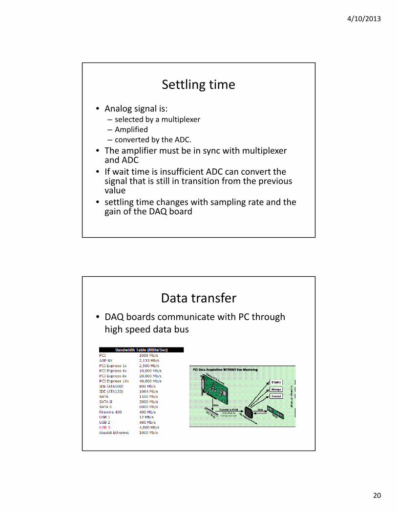
Data transfer• DAQ boards communicate with PC through high speed data bus
4/10/2013
21
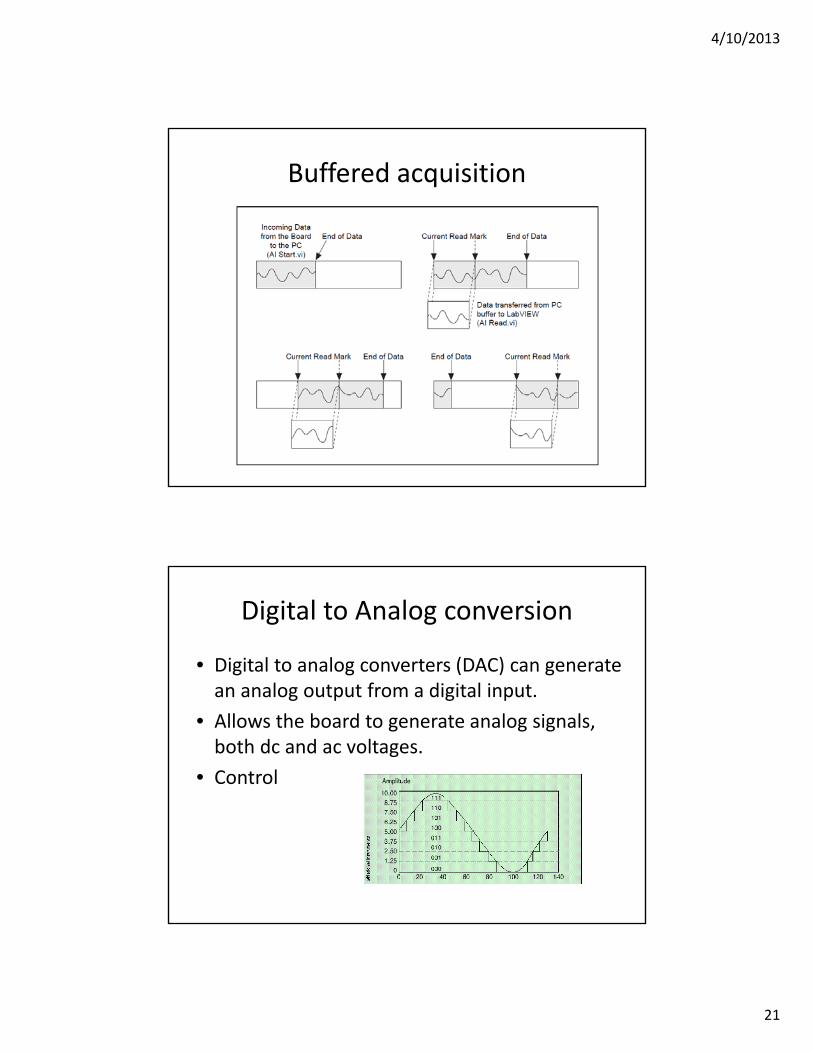
Buffered acquisition
Digital to Analog conversion
• Digital to analog converters (DAC) can generate an analog output from a digital input.
• Allows the board to generate analog signals, both dc and ac voltages.
• Control
4/10/2013
22
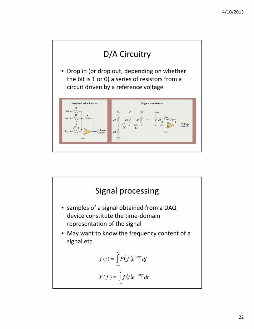
D/A Circuitry
• Drop in (or drop out, depending on whether the bit is 1 or 0) a series of resistors from a circuit driven by a reference voltage
Signal processing
• samples of a signal obtained from a DAQ device constitute the time‐domain representation of the signal
• May want to know the frequency content of a signal etc.
4/10/2013
23
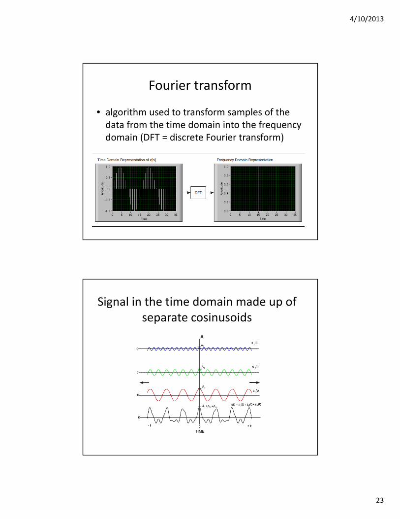
Fourier transform
• algorithm used to transform samples of the data from the time domain into the frequency domain (DFT = discrete Fourier transform)
Signal in the time domain made up of separate cosinusoids
4/10/2013
24
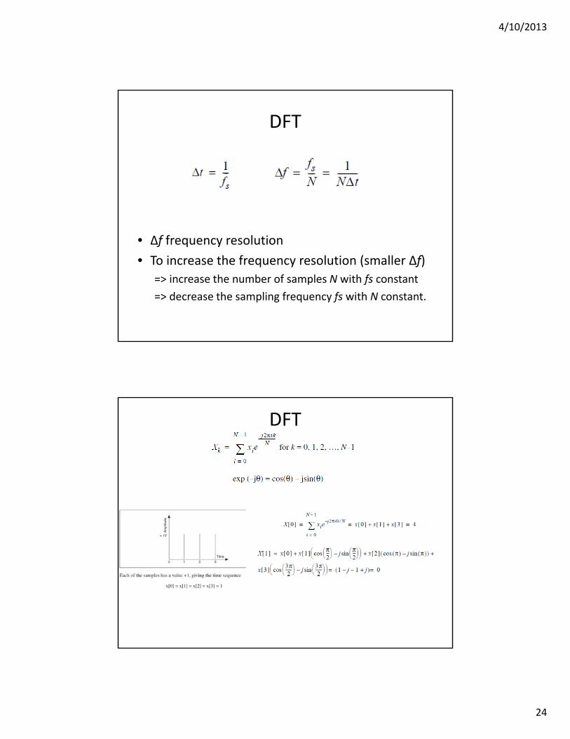
DFT
• Δf frequency resolution
• To increase the frequency resolution (smaller Δf)
=> increase the number of samples N with fs constant
=> decrease the sampling frequency fs with N constant.
DFT
4/10/2013
25
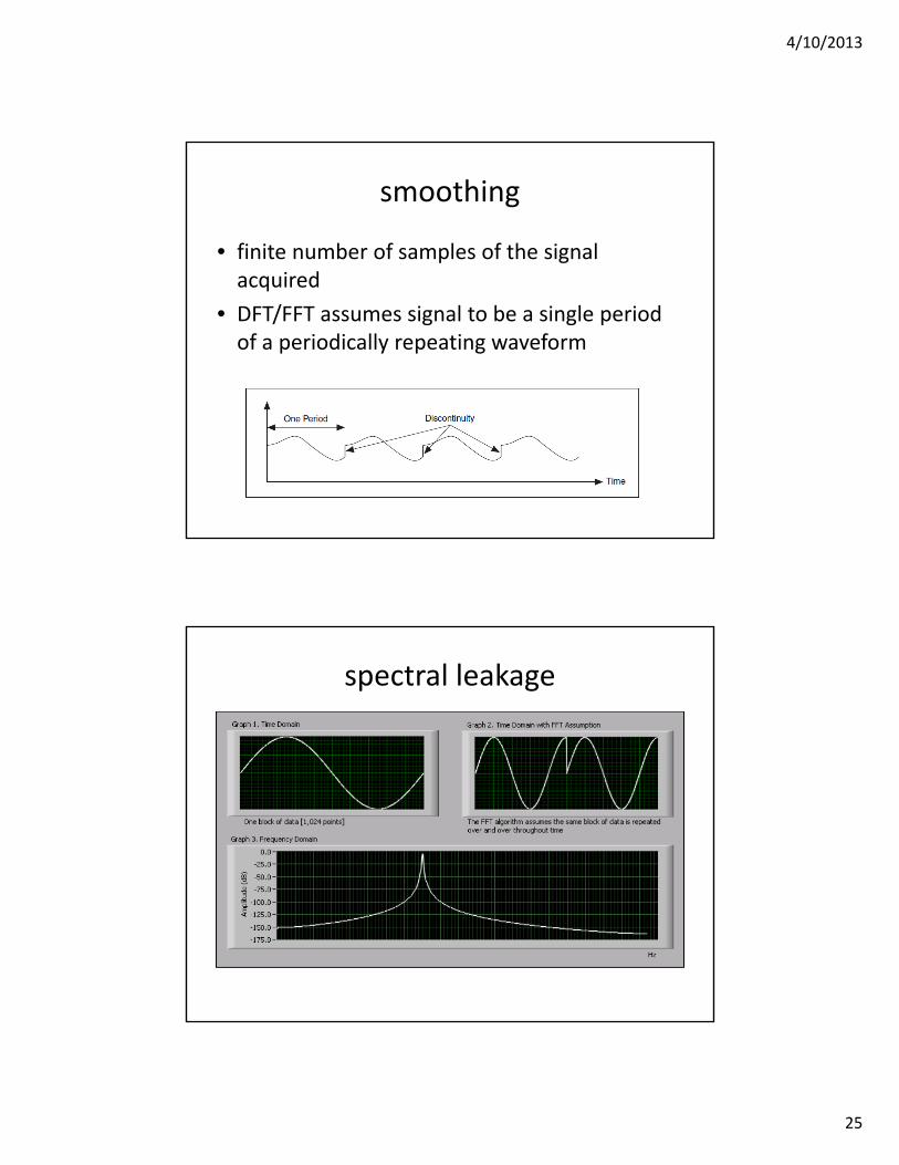
smoothing
• finite number of samples of the signal acquired
• DFT/FFT assumes signal to be a single period of a periodically repeating waveform
spectral leakage
4/10/2013
26
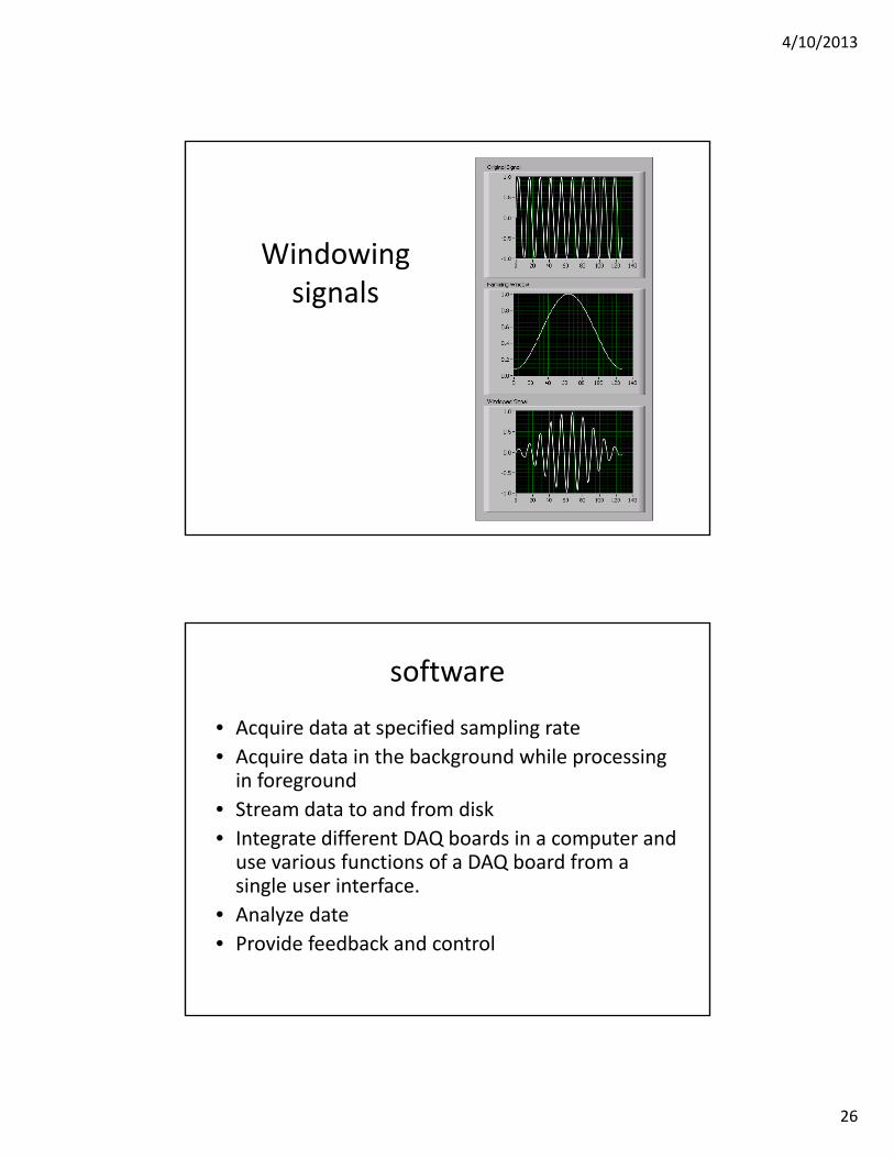
Windowing signals
software
• Acquire data at specified sampling rate
• Acquire data in the background while processing in foreground
• Stream data to and from disk
• Integrate different DAQ boards in a computer and use various functions of a DAQ board from a single user interface.
• Analyze date
• Provide feedback and control
4/10/2013
27
Virtual instruments
• LabVIEW programs are called virtual instruments, or VIs
• appearance and operation imitate physical instruments, such as oscilloscopes and multimeters.
• VI uses functions that manipulate input from the user interface or other sources and display that information
• move or store files to locations or computers.
Components of a VI
A VI contains the following three components:• Front panel—Serves as the user interface.• Block diagram—Contains the graphical source code that defines the functionality of the VI.• Icon and connector pane—Identifies the interface to the VI so that you can use the VI in another VI. A VI within another VI is called a subVI. A subVI corresponds to a subroutine in text‐based programming languages.
4/10/2013
28
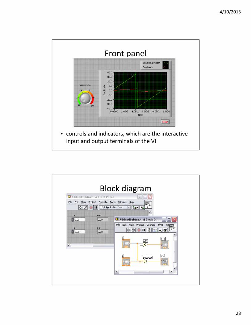
Front panel
• controls and indicators, which are the interactive input and output terminals of the VI
Block diagram
4/10/2013
29
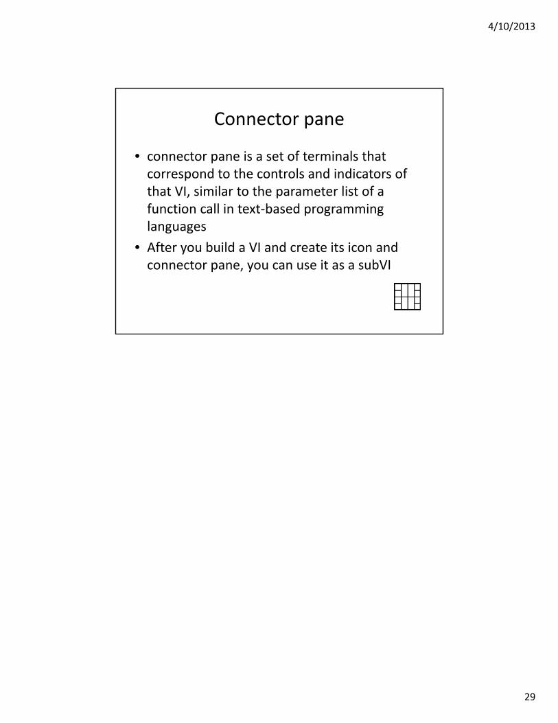
Connector pane
• connector pane is a set of terminals that correspond to the controls and indicators of that VI, similar to the parameter list of a function call in text‐based programming languages
• After you build a VI and create its icon and connector pane, you can use it as a subVI


![Social Networks, Information Acquisition, and Asset Pricesheuristic.kaist.ac.kr/.../[8]SocialNetwork_InformationAcquisition.pdf · Social Networks, Information Acquisition, and Asset](https://static.fdocument.pub/doc/165x107/5c67397909d3f2bb148b58fc/social-networks-information-acquisition-and-asset-8socialnetworkinformationacquisitionpdf.jpg)