Elektronik ve Haberleşme Mühendisliği Bölümü Elektrik-Elektronik Fakültesi
Upload
truongxuyenCategory
view
214download
0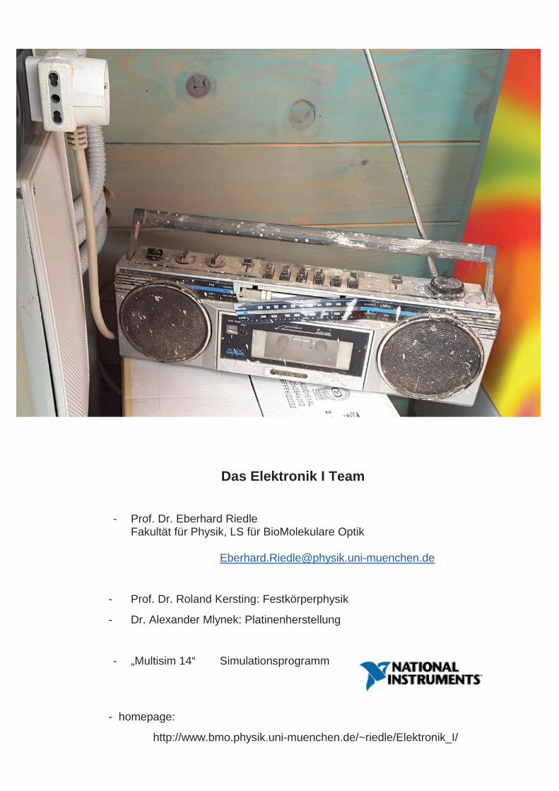
Das Elektronik I Team
- Prof. Dr. Eberhard Riedle Fakultät für Physik, LS für BioMolekulare Optik
- Prof. Dr. Roland Kersting: Festkörperphysik
- Dr. Alexander Mlynek: Platinenherstellung
- „Multisim 14“ Simulationsprogramm
- homepage:
http://www.bmo.physik.uni-muenchen.de/~riedle/Elektronik_I/

bisher 75 x zitiert
Dye Laser
Single FrequencyArgon Ion Laser
StabilisedHeNe Laser
PolarizingBeamsplitter
PolarizingBeamsplitter
BSTo Experiment
IF1
IF2
IF3
He Ne Detector
Dye Laser Detector
Argon Ion LaserDetector
M
M
M
M
M
L1 L2F.P.I.
figure 1 E. Riedle et al., ’Stabilization and ...’
Stabilization of the Difference Frequency Spectrometer
Fabry-Perot Interferometer
StabilizedHe Ne Laser
Conditioning
FilterDouble BalancedMixerPhase Shifter
Local Oscillatorν = 4.4kHz
Proportional τ = 1s
Integral τ = 100s
Heater Control
Working Point
Proportional τ = 0.003s
PZT Control
PZT Heater
AC Component
Detector
Locking of The Transfer Cavity
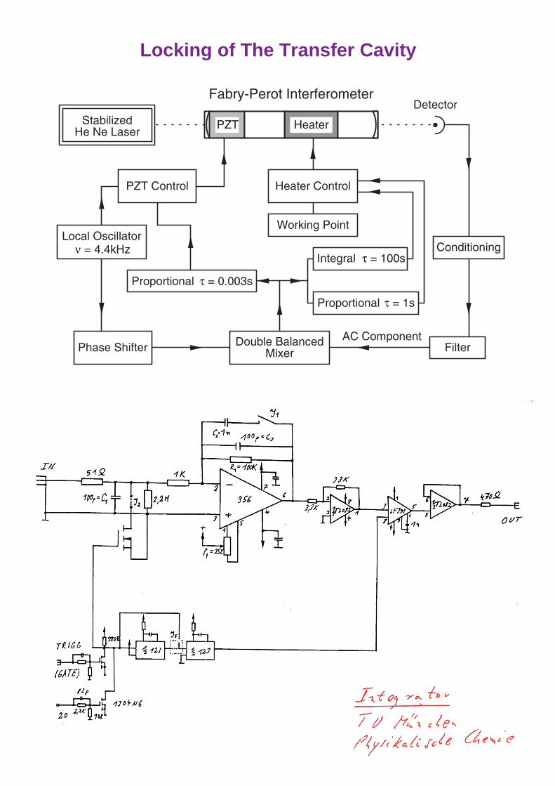
QYDS electronics : shutter control and I/U converter for solar cell
Elektronik I, WS 201 /1 (E. Riedle)
0. Vorstellung und Einleitung
I. Lineare passive Bauelemente 1) Grundbegriffe, Widerstände, Kondensatoren, Spulen2) Lineare Netzwerke - Reduzierung, Wheatstone'sche Brücke 3) Komplexe Amplituden in linearen Netzwerken4) Anwendungen und Beispiele - Filterschaltungen, Schwingkreise
II. Netzwerke mit aktiven Bauelementen1) Aktive Bauelemente - Spannungs- und Stromquelle, Ersatzschaltbilder2) Zweipolquelle3) Kreisstromverfahren, Knotenspannungen, Numerische Verfahren4) Vierpole - Transformator, Vierpol- oder Filterkette 5) Leitungen, HF-Leitungen, Leitungstransformator etc.
- Reflexion, Transmission - Anwendungen: kurze Pulse, Impedanztransformatoren - Oberflächenwellen, HF-Filter
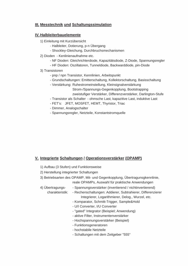
III. Messtechnik und Schaltungssimulation
IV. Halbleiterbauelemente 1) Einleitung mit Kurzübersicht - Halbleiter, Dotierung, p-n Übergang - Shockley-Gleichung, Durchbruchsmechanismen 2) Dioden - Kenlinienaufnahme etc. - NF Dioden: Gleichrichterdiode, Kapazitätsdiode, Z-Diode, Spannungsregler - HF Dioden: Oszillatoren, Tunneldiode, Backwarddiode, pin-Diode 3) Transistoren - pnp / npn Transistor, Kennlinien, Arbeitspunkt - Grundschaltungen: Emitterschaltung, Kollektorschaltung, Basisschaltung - Verstärkung: Ruhestromeinstellung, Kleinsignalverstärkung Strom-/Spannungs-Gegenkopplung, Bootstrapping zweistufiger Verstärker, Differenzverstärker, Darlington-Stufe - Transistor als Schalter - ohmsche Last, kapazitive Last, induktive Last - FET’s: JFET, MOSFET, HEMT, Thyristor, Triac - Dimmer, Analogschalter - Spannungsregler, Netzteile, Konstantstromquelle
V. Integrierte Schaltungen / Operationsverstärker (OPAMP)
1) Aufbau (3 Stufen) und Funktionsweise 2) Herstellung integrierter Schaltungen 3) Betriebsarten des OPAMP, Mit- und Gegenkopplung, Übertragunsgkennlinie, reale OPAMPs, Auswahl für praktische Anwendungen 4) Übertragungs- - Spannungsverstärker (invertierend / nichtinvertierend) charakteristik: - Rechenschaltungen: Addierer, Subtrahierer, Differenzierer Integrierer, Logarithmierer, Delog., Wurzel, etc. - Komparator, Schmitt-Trigger, Sample&Hold - U/I Converter, I/U Converter - "gated" Integrator (Beispiel; Anwendung) - aktive Filter, Instrumentenverstärker - Hochspannungsverstärker (Beispiel) - Funktionsgeneratoren - hochstabile Netzteile - Schaltungen mit dem Zeitgeber "555"
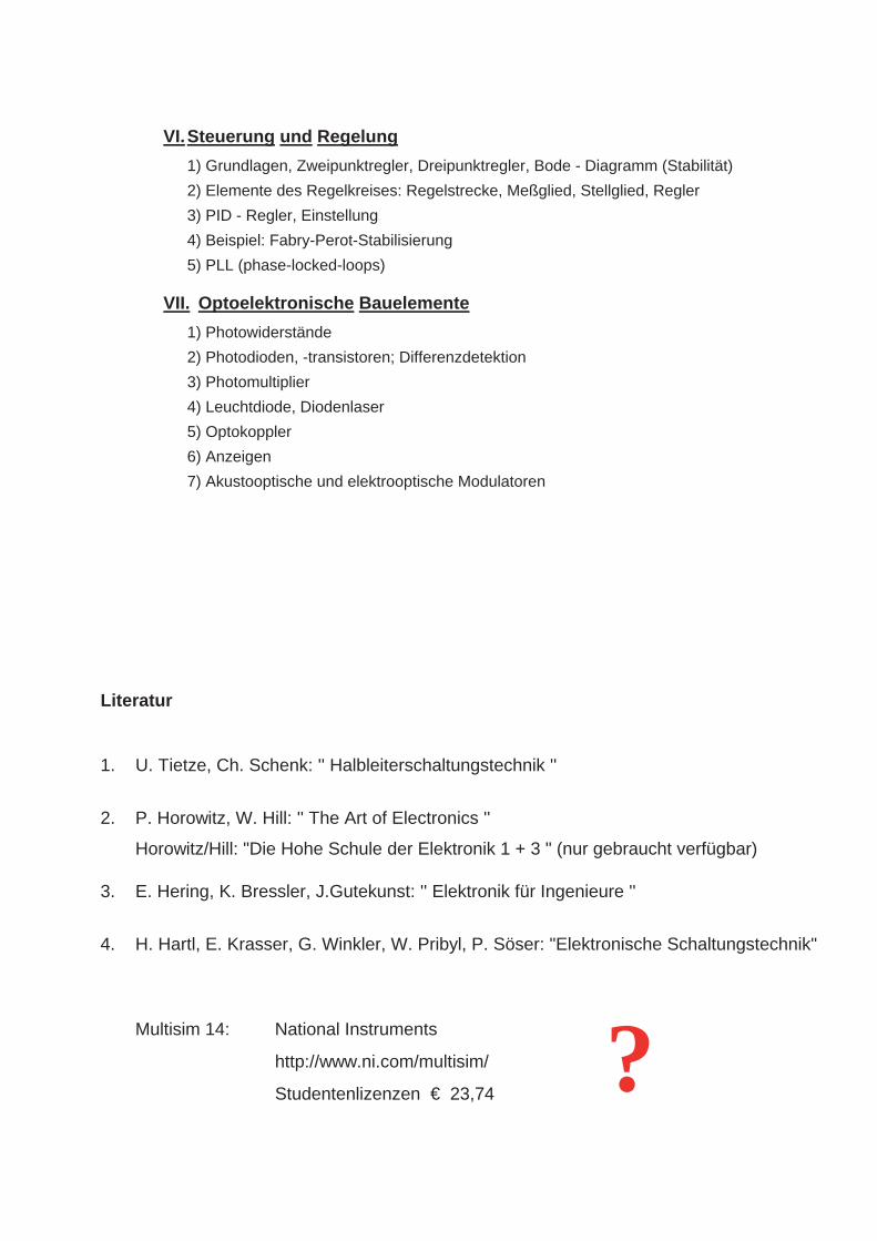
VI. Steuerung und Regelung 1) Grundlagen, Zweipunktregler, Dreipunktregler, Bode - Diagramm (Stabilität) 2) Elemente des Regelkreises: Regelstrecke, Meßglied, Stellglied, Regler 3) PID - Regler, Einstellung 4) Beispiel: Fabry-Perot-Stabilisierung 5) PLL (phase-locked-loops)
VII. Optoelektronische Bauelemente 1) Photowiderstände 2) Photodioden, -transistoren; Differenzdetektion 3) Photomultiplier 4) Leuchtdiode, Diodenlaser 5) Optokoppler 6) Anzeigen 7) Akustooptische und elektrooptische Modulatoren
Literatur
1. U. Tietze, Ch. Schenk: '' Halbleiterschaltungstechnik ''
2. P. Horowitz, W. Hill: '' The Art of Electronics ''
Horowitz/Hill: "Die Hohe Schule der Elektronik 1 + 3 " (nur gebraucht verfügbar)
3. E. Hering, K. Bressler, J.Gutekunst: '' Elektronik für Ingenieure ''
4. H. Hartl, E. Krasser, G. Winkler, W. Pribyl, P. Söser: "Elektronische Schaltungstechnik"
Multisim 14: National Instruments
http://www.ni.com/multisim/
Studentenlizenzen € 23,74 ?

TL�H
�5646
LF155�LF156�LF157 Series Monolithic JFET Input Operational Amplifiers
Decem
ber1994
LF155�LF156�LF157
Series
Monolith
icJFET
InputO
pera
tionalA
mplifiers
Genera
lD
escription
These
are
the
firs
tm
onolit
hic
JFET
inputopera
tionalam
pli-
fiers
toin
corp
ora
tew
ell
matc
hed�hig
hvoltage
JFETs
on
the
sam
echip
with
sta
ndard
bip
ola
rtransis
tors
(BI-FET
TM
Tech-
nolo
gy)
�These
am
plif
iers
featu
relo
win
put
bia
sand
offset
currents
�lo
woffsetvoltage
and
offsetvoltage
drift�couple
d
with
offsetadju
stw
hic
hdoes
notdegra
de
drift
orcom
mon-
mode
reje
ction�The
devic
es
are
als
odesig
ned
forhig
hsle
w
rate
�w
ide
bandw
idth
�extrem
ely
fastsettlin
gtim
e�lo
wvolt-
age
and
currentnois
eand
alo
w1�fnois
ecorn
er�
Advanta
ges
YR
epla
ce
expensiv
ehyb
rid
and
module
FET
op
am
ps
YR
ugged
JFETs
allo
wblo
w-o
ut
free
handlin
gcom
pare
d
with
MO
SFET
inputdevic
es
YExcelle
nt
for
low
nois
eapplic
ations
usin
geither
hig
hor
low
sourc
eim
pedance�
very
low
1�fcorn
er
YO
ffset
adju
st
does
not
degra
de
drift
or
com
mon-m
ode
reje
ction
as
inm
ostm
onolit
hic
am
plif
iers
YN
ew
outp
ut
sta
ge
allo
ws
use
of
larg
ecapacitiv
elo
ads
(5�0
00
pF)
withoutsta
bility
pro
ble
ms
YIn
tern
al
com
pensation
and
larg
ediffe
rential
input
volt-
age
capability
Applications
YPre
cis
ion
hig
hspeed
inte
gra
tors
YFastD
�A
and
A�D
converters
YH
igh
impedance
buffers
YW
ideband�lo
wnois
e�lo
wdrift
am
plif
iers
YLogarith
mic
am
plif
iers
YPhoto
cell
am
plif
iers
YSam
ple
and
Hold
circuits
Com
mon
Featu
res
(LF155A
�LF156A
�LF157A
)Y
Low
inputbia
scurrent
30
pA
YLow
InputO
ffsetC
urrent
3pA
YH
igh
inputim
pedance
1012X
YLow
inputoffsetvoltage
1m
VY
Low
inputoffsetvoltage
tem
p�drift
3m
V��C
YLow
inputnois
ecurrent
0�0
1pA
�0H
zY
Hig
hcom
mon-m
ode
reje
ction
ratio
100
dB
YLarg
edc
voltage
gain
106
dB
Uncom
mon
Featu
res
YExtrem
ely
fastsettlin
g
tim
eto
0�0
1%
YFastsle
w
rate
YW
ide
gain
bandw
idth
YLow
input
nois
evoltage
LF155A
LF156A
LF157A
Units
(AV
e5)
41�5
1�5
ms
512
50
V�m
s
2�5
520
MH
z
20
12
12
nV�0H
z
Sim
plified
Schem
atic
�3pF
inLF157
series�
TL�H
�5646–1
BI-FET
TM�B
I-FET
IITM
are
tradem
ark
sofN
ationalSem
iconducto
rC
orp
ora
tion�
C1995
NationalS
em
iconducto
rC
orp
ora
tion
RR
D-B
30M
115�Printe
din
U�S�A
�
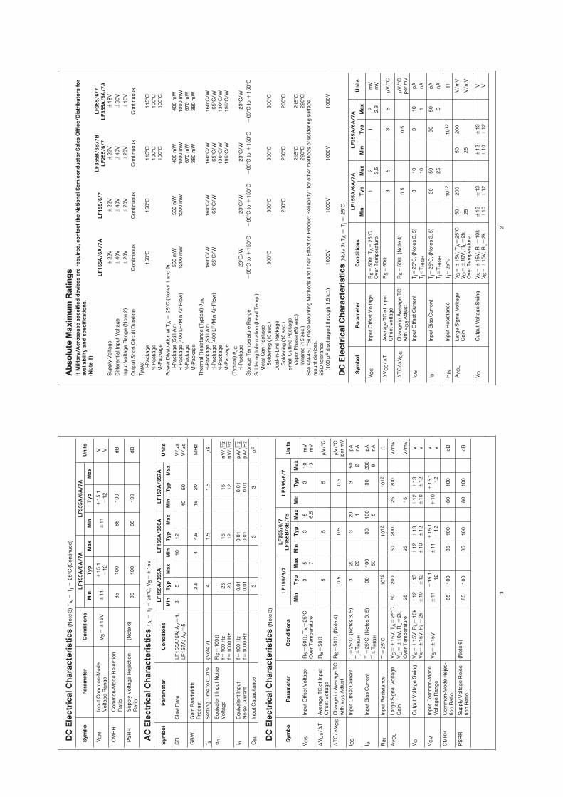
Absolu
teM
axim
um
Ratings
IfM
ilitary
�A
ero
space
specifie
ddevic
es
are
required�conta
ctth
eN
ationalSem
iconducto
rSale
sO
ffic
e�D
istr
ibuto
rsfo
r
availability
and
specific
ations�
(Note
8)
LF155A
�6A
�7A
LF155�6�7
LF355B
�6B
�7B
LF355�6�7
LF255�6�7
LF355A
�6A
�7A
Supply
Voltage
g22V
g22V
g22V
g18V
Diffe
rentialI
nputVoltage
g40V
g40V
g40V
g30V
InputVoltage
Range
(Note
2)
g20V
g20V
g20V
g16V
Outp
utShort
Circuit
Dura
tion
Continuous
Continuous
Continuous
Continuous
TjM
AX
H-P
ackage
150�C
150�C
115�C
115�C
N-P
ackage
100�C
100�C
M-P
ackage
100�C
100�C
Pow
erD
issip
ation
atT
Ae
25�C
(Note
s1
and
9)
H-P
ackage
(Still
Air)
560
mW
560
mW
400
mW
400
mW
H-P
ackage
(400
LF�M
inA
irFlo
w)
1200
mW
1200
mW
1000
mW
1000
mW
N-P
ackage
670
mW
670
mW
M-P
ackage
380
mW
380
mW
Therm
alR
esis
tance
(Typ
ical)
iJA
H-P
ackage
(Still
Air)
160�C
�W
160�C
�W
160�C
�W
160�C
�W
H-P
ackage
(400
LF�M
inA
irFlo
w)
65�C
�W
65�C
�W
65�C
�W
65�C
�W
N-P
ackage
130�C
�W
130�C
�W
M-P
ackage
195�C
�W
195�C
�W
(Typ
ical)
iJC
H-P
ackage
23�C
�W
23�C
�W
23�C
�W
23�C
�W
Sto
rage
Tem
pera
ture
Range
b65�C
toa
150�C
b65�C
toa
150�C
b65�C
toa
150�C
b65�C
toa
150�C
Sold
ering
Info
rmation
(Lead
Tem
p�)
Meta
lCan
Package
Sold
ering
(10
sec�)
300�C
300�C
300�C
300�C
Dual-In
-Lin
ePackage
Sold
ering
(10
sec�)
260�C
260�C
260�C
Sm
all
Outlin
ePackage
VaporPhase
(60
sec�)
215�C
215�C
Infrare
d(1
5sec�)
220�C
220�C
See
AN
-450
‘‘Surface
Mounting
Meth
ods
and
Their
Effecton
Pro
ductR
elia
bility
’’fo
roth
erm
eth
ods
ofsold
ering
surface
mountdevic
es�
ESD
tole
rance
(100
pF
dis
charg
ed
thro
ugh
1�5
kX
)1000V
1000V
1000V
1000V
DC
Ele
ctr
icalC
hara
cte
ristics
(Note
3)T
Ae
Tje
25�C
Sym
bol
Para
mete
rC
onditio
ns
LF155A
�6A
�7A
LF355A
�6A
�7A
Units
Min
Typ
Max
Min
Typ
Max
VO
SIn
putO
ffsetVoltage
RSe
50X
�T
Ae
25�C
12
12
mV
OverTem
pera
ture
2�5
2�3
mV
DV
OS�D
TA
vera
ge
TC
ofIn
put
RSe
50X
35
35
mV��C
OffsetVoltage
DTC
�D
VO
SC
hange
inA
vera
ge
TC
RSe
50X
�(N
ote
4)
0�5
0�5
mV��C
with
VO
SA
dju
st
perm
V
I OS
InputO
ffsetC
urrent
Tje
25�C
�(N
ote
s3�5)
310
310
pA
Tjs
TH
IGH
10
1nA
I BIn
putB
ias
Current
Tje
25�C
�(N
ote
s3�5)
30
50
30
50
pA
Tjs
TH
IGH
25
5nA
RIN
InputR
esis
tance
Tje
25�C
1012
1012
X
AVO
LLarg
eSig
nalV
oltage
VSe
g15V�T
Ae
25�C
50
200
50
200
V�m
VG
ain
VO
eg
10V�R
Le
2k
25
25
V�m
VO
verTem
pera
ture
VO
Outp
utVoltage
Sw
ing
VSe
g15V�R
Le
10k
g12
g13
g12
g13
VV
Se
g15V�R
Le
2k
g10
g12
g10
g12
V
2
DC
Ele
ctr
icalC
hara
cte
ristics
(Note
3)T
Ae
Tje
25�C
(Continued)
Sym
bol
Para
mete
rC
onditio
ns
LF155A
�6A
�7A
LF355A
�6A
�7A
Units
Min
Typ
Max
Min
Typ
Max
VC
MIn
putC
om
mon-M
ode
VSe
g15V
g11
a15�1
g11
a15�1
V
Voltage
Range
b12
b12
V
CM
RR
Com
mon-M
ode
Reje
ction
85
100
85
100
dB
Ratio
PSR
RSupply
Voltage
Reje
ction
(Note
6)
85
100
85
100
dB
Ratio
AC
Ele
ctr
icalC
hara
cte
ristics
TA
eT
je
25�C
�V
Se
g15V
Sym
bol
Para
mete
rC
onditio
ns
LF155A
�355A
LF156A
�356A
LF157A
�357A
Units
Min
Typ
Max
Min
Typ
Max
Min
Typ
Max
SR
Sle
wR
ate
LF155A
�6A
�A
Ve
1�
35
10
12
V�m
s
LF157A
�A
Ve
540
50
V�m
s
GB
WG
ain
Bandw
idth
2�5
44�5
15
20
MH
zPro
duct
t sSettlin
gTim
eto
0�0
1%
(Note
7)
41�5
1�5
ms
en
Equiv
ale
ntIn
putN
ois
eR
Se
100X
Voltage
fe100
Hz
25
15
15
nV�0H
z
fe1000
Hz
20
12
12
nV�0H
z
i nEquiv
ale
ntIn
put
fe100
Hz
0�0
10�0
10�0
1pA
�0H
z
Nois
eC
urrent
fe1000
Hz
0�0
10�0
10�0
1pA
�0H
z
CIN
InputC
apacitance
33
3pF
DC
Ele
ctr
icalC
hara
cte
ristics
(Note
3)
Sym
bol
Para
mete
rC
onditio
ns
LF155�6�7
LF255�6�7
LF355�6�7
Units
LF355B
�6B
�7B
Min
Typ
Max
Min
Typ
Max
Min
Typ
Max
VO
SIn
putO
ffsetVoltage
RSe
50X
�T
Ae
25�C
35
35
310
mV
OverTem
pera
ture
76�5
13
mV
DV
OS�D
TA
vera
ge
TC
ofIn
put
RSe
50X
55
5m
V��C
OffsetVoltage
DTC
�D
VO
SC
hange
inA
vera
ge
TC
RSe
50X
�(N
ote
4)
0�5
0�5
0�5
mV��C
with
VO
SA
dju
st
perm
V
I OS
InputO
ffsetC
urrent
Tje
25�C
�(N
ote
s3�5)
320
320
350
pA
Tjs
TH
IGH
20
12
nA
I BIn
putB
ias
Current
Tje
25�C
�(N
ote
s3�5)
30
100
30
100
30
200
pA
Tjs
TH
IGH
50
58
nA
RIN
InputR
esis
tance
Tje
25�C
1012
1012
1012
X
AVO
LLarg
eSig
nalV
oltage
VSe
g15V�T
Ae
25�C
50
200
50
200
25
200
V�m
V
Gain
VO
eg
10V�R
Le
2k
OverTem
pera
ture
25
25
15
V�m
V
VO
Outp
utVoltage
Sw
ing
VSe
g15V�R
Le
10k
g12
g13
g12
g13
g12
g13
V
VSe
g15V�R
Le
2k
g10
g12
g10
g12
g10
g12
V
VC
MIn
putC
om
mon-M
ode
VSe
g15V
g11
a15�1
g11
g15�1
a10
a15�1
V
Voltage
Range
b12
b12
b12
V
CM
RR
Com
mon-M
ode
Reje
c-
85
100
85
100
80
100
dB
tion
Ratio
PSR
RSupply
Voltage
Reje
c-
(Note
6)
85
100
85
100
80
100
dB
tion
Ratio
3
DC
Ele
ctr
icalC
hara
cte
ristics
TA
eT
je
25�C
�V
Se
g15V
LF155A
�155�
LF156A
�156�
LF157A
�157
Para
mete
rLF255�
LF355
LF256�356B
LF356A
�356
LF257�357B
LF357A
�357
Units
LF355A
�355B
Typ
Max
Typ
Max
Typ
Max
Typ
Max
Typ
Max
Typ
Max
Supply
Current
24
24
57
510
57
510
mA
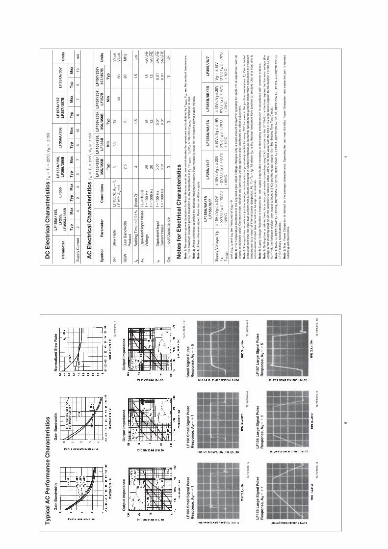
AC
Ele
ctr
icalC
hara
cte
ristics
TA
eT
je
25�C
�V
Se
g15V
LF155�255�
LF156�256�
LF156�256�
LF157�257�
LF157�257�
Sym
bol
Para
mete
rC
onditio
ns
355�355B
LF356B
356�356B
LF357B
357�357B
Units
Typ
Min
Typ
Min
Typ
SR
Sle
wR
ate
LF155�6�A
Ve
1�
57�5
12
V�m
s
LF157�A
Ve
530
50
V�m
s
GB
WG
ain
Bandw
idth
2�5
520
MH
z
Pro
duct
t sSettlin
gTim
eto
0�0
1%
(Note
7)
41�5
1�5
ms
en
Equiv
ale
ntIn
putN
ois
eR
Se
100X
Voltage
fe100
Hz
25
15
15
nV�0H
z
fe1000
Hz
20
12
12
nV�0H
z
i nEquiv
ale
ntIn
put
fe100
Hz
0�0
10�0
10�0
1pA
�0H
z
CurrentN
ois
efe
1000
Hz
0�0
10�0
10�0
1pA
�0H
z
CIN
InputC
apacitance
33
3pF
Note
sfo
rEle
ctr
icalC
hara
cte
ristics
Note
1�The
maxim
um
pow
erdis
sip
ation
forth
ese
devic
es
mustbe
dera
ted
atele
vate
dte
mpera
ture
sand
isdic
tate
dby
TjM
AX�i
jA�and
the
am
bie
ntte
mpera
ture
�
TA�The
maxim
um
availa
ble
pow
erdis
sip
ation
atany
tem
pera
ture
isP
de
(TjM
AXb
TA)�
ijA
orth
e25�C
PdM
AX�w
hic
heveris
less�
Note
2�U
nle
ss
oth
erw
ise
specifie
dth
eabsolu
tem
axim
um
negative
inputvoltage
isequalto
the
negative
pow
ersupply
voltage�
Note
3�U
nle
ss
oth
erw
ise
sta
ted�th
ese
testconditio
ns
apply
�
LF155A
�6A
�7A
LF255��6�7
LF355A
�6A
�7A
LF355B
�6B
�7B
LF355��6�7
LF155��6�7
Supply
Voltage�V
Sg
15V
sV
Ss
g20V
g15V
sV
Ss
g20V
g15V
sV
Ss
g18V
g15V
sV
Sg
20V
VSe
g15V
TA
b55�C
sT
As
a125�C
b25�C
sT
As
a85�C
0�C
sT
As
a70�C
0�C
sT
As
a70�C
0�C
sT
As
a70�C
TH
IGH
a125�C
a85�C
a70�C
a70�C
a70�C
and
VO
S�I B
and
I OS
are
measure
datV
CM
e0�
Note
4�The
Tem
pera
ture
Coeffic
ientofth
eadju
ste
din
putoffsetvoltage
changes
only
asm
all
am
ount(0
�5m
V��C
typic
ally
)fo
reach
mV
ofadju
stm
entfrom
its
origin
alunadju
ste
dvalu
e�C
om
mon-m
ode
reje
ction
and
open
loop
voltage
gain
are
als
ounaffecte
dby
offsetadju
stm
ent�
Note
5�The
inputbia
scurrents
are
junction
leakage
currents
whic
happro
xim
ate
lydouble
forevery
10�C
incre
ase
inth
eju
nction
tem
pera
ture
�T
J�D
ue
tolim
ited
pro
duction
testtim
e�th
ein
putbia
scurrents
measure
dare
correla
ted
toju
nction
tem
pera
ture
�In
norm
alopera
tion
the
junction
tem
pera
ture
rises
above
the
am
bie
nt
tem
pera
ture
as
are
sult
of
inte
rnalpow
er
dis
sip
ation�Pd�T
jeT
Aa
ijA
Pd
where
ijA
isth
eth
erm
alre
sis
tance
from
junction
toam
bie
nt�
Use
of
aheat
sin
kis
recom
mended
ifin
putbia
scurrentis
tobe
keptto
am
inim
um
�
Note
6�Supply
Voltage
Reje
ction
ism
easure
dfo
rboth
supply
magnitudes
incre
asin
gordecre
asin
gsim
ultaneously
�in
accord
ance
with
com
mon
pra
ctice�
Note
7�Settlin
gtim
eis
defined
here
�fo
ra
unity
gain
inverter
connection
usin
g2
kX
resis
tors
for
the
LF155�6�It
isth
etim
ere
quired
for
the
error
voltage
(the
voltage
atth
ein
vertin
gin
putpin
on
the
am
plif
ier)
tosettle
tow
ithin
0�0
1%
ofits
finalvalu
efrom
the
tim
ea
10V
ste
pin
putis
applie
dto
the
inverter�
Forth
eLF157�
AVe
b5�th
efe
edback
resis
torfrom
outp
utto
inputis
2kX
and
the
outp
utste
pis
10V
(See
Settlin
gTim
eTestC
ircuit)�
Note
8�R
efe
rto
RETS155A
Xfo
rLF155A
�R
ETS155X
for
LF155�R
ETS156A
Xfo
rLF156A
�R
ETS156X
for
LF156�R
ETS157A
for
LF157A
and
RETS157X
for
LF157
milita
ryspecific
ations�
Note
9�M
ax�Pow
er
Dis
sip
ation
isdefined
by
the
package
chara
cte
ristics�O
pera
ting
the
part
near
the
Max�Pow
er
Dis
sip
ation
may
cause
the
part
toopera
te
outs
ide
guara
nte
ed
limits�
4
Typic
alA
CPerf
orm
ance
Chara
cte
ristics
Gain
Bandw
idth
Gain
Bandw
idth
Norm
alized
Sle
wR
ate TL�H
�5646–4
Outp
utIm
pedance
Outp
utIm
pedance
Outp
utIm
pedance
TL�H
�5646–12
LF155
Sm
all
Sig
nalPuls
e
Response�A
Ve
a1
TL�H
�5646–5
LF156
Sm
all
Sig
nalPuls
e
Response�A
Ve
a1
TL�H
�5646–6
Sm
all
Sig
nalPuls
e
Response�A
Ve
a5
TL�H
�5646–7
LF155
Larg
eSig
nalPuls
e
Response�A
Ve
a1
TL�H
�5646–8
LF156
Larg
eSig
nalPuls
e
Response�A
Ve
a1
TL�H
�5646–9
LF157
Larg
eSig
nalPuls
e
Response�A
Ve
a5
TL�H
�5646–10
6
Deta
iled
Schem
atic
�Ce
3pF
inLF157
series�
TL�H
�5646–13
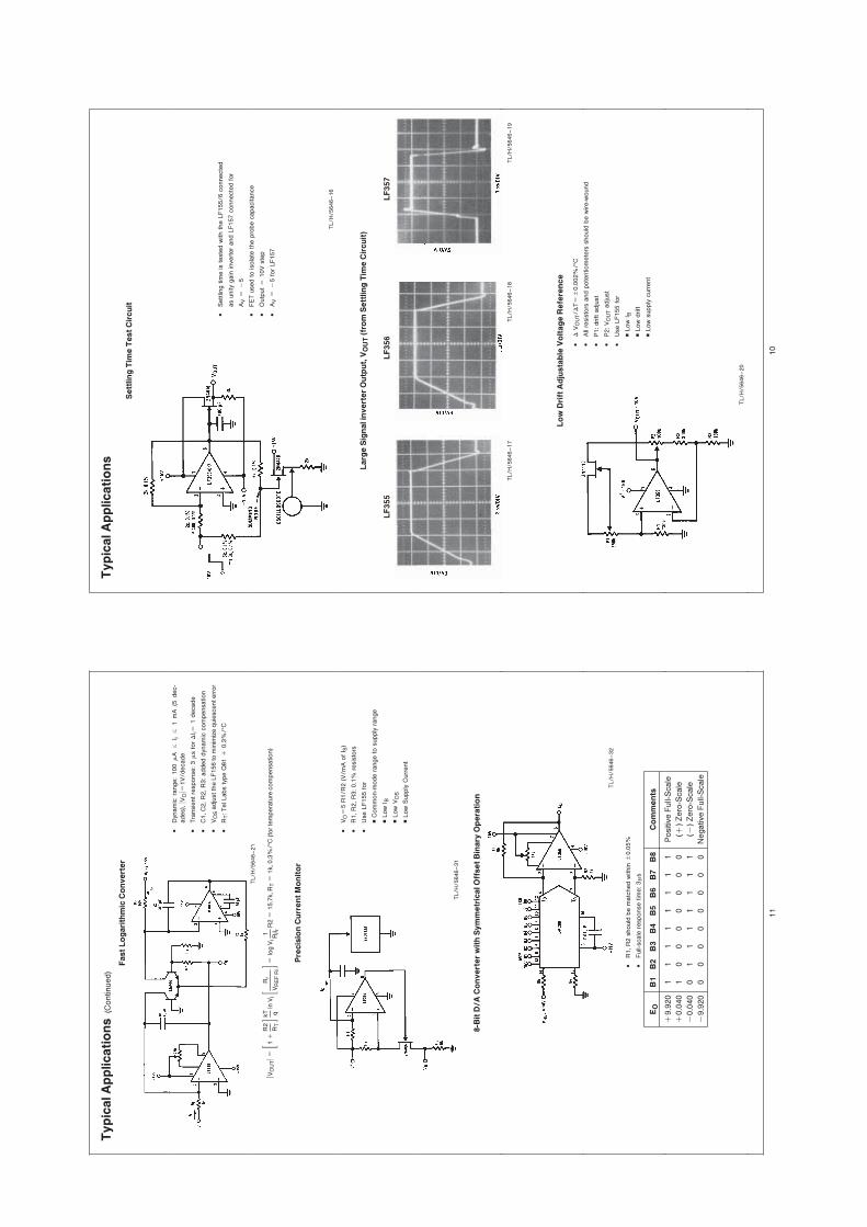
Connection
Dia
gra
ms
(Top
Vie
ws)
Meta
lC
an
Package
(H)
TL�H
�5646–14
Ord
erN
um
berLF156A
H�LF155H
�LF156H
�LF255H
�
LF256H
�LF257H
�LF355A
H�LF356A
H�
LF357A
H�LF356B
H�LF355H
�LF356H
�
LF357H
�LM
155A
H�883�LM
155H
�883�LM
156A
H�883�
LM
156H
�883�LM
157A
H�883
orLM
157H
�883�
See
NS
Package
Num
berH
08C
Dual-In
-Lin
ePackage
(Mand
N)
TL�H
�5646–29
Ord
erN
um
berLF355M
�LF356M
�LF357M
�LF355B
M�
LF356B
M�LF355B
N�LF356B
N�LF357B
N�LF355N
�
LF356N
orLF357N
See
NS
Package
Num
berM
08A
orN
08E
�Availa
ble
perJM
38510�11401
orJM
38510�11402
8
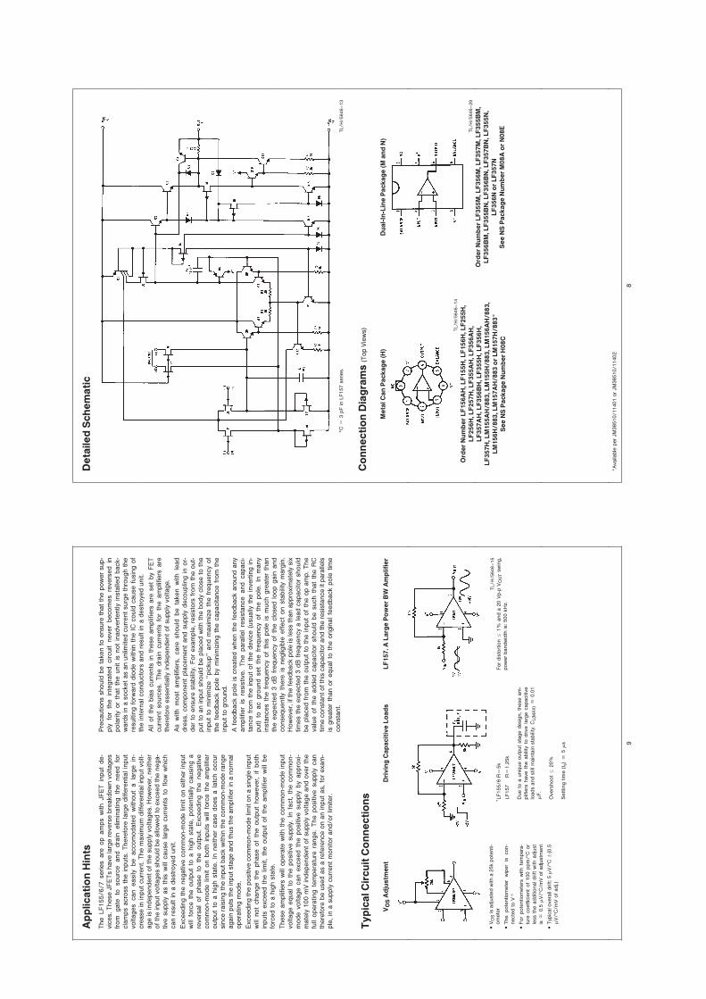
Application
Hin
ts
The
LF155�6�7
series
are
op
am
ps
with
JFET
input
de-
vic
es�These
JFETs
have
larg
ere
vers
ebre
akdow
nvoltages
from
gate
tosourc
eand
dra
inelim
inating
the
need
for
cla
mps
acro
ss
the
inputs
�There
fore
larg
ediffe
rentialin
put
voltages
can
easily
be
accom
odate
dw
ithout
ala
rge
in-
cre
ase
inin
putcurrent�
The
maxim
um
diffe
rentialin
putvolt-
age
isin
dependentofth
esupply
voltages�H
ow
ever�
neither
ofth
ein
putvoltages
should
be
allo
wed
toexceed
the
nega-
tive
supply
as
this
will
cause
larg
ecurrents
toflow
whic
h
can
result
ina
destroye
dunit�
Exceedin
gth
enegative
com
mon-m
ode
limit
on
either
input
will
forc
eth
eoutp
ut
toa
hig
hsta
te�
pote
ntially
causin
ga
revers
al
of
phase
toth
eoutp
ut�
Exceedin
gth
enegative
com
mon-m
ode
limit
on
both
inputs
will
forc
eth
eam
plif
ier
outp
ut
toa
hig
hsta
te�
Inneither
case
does
ala
tch
occur
sin
ce
rais
ing
the
inputback
within
the
com
mon-m
ode
range
again
puts
the
inputsta
ge
and
thus
the
am
plif
ierin
anorm
al
opera
ting
mode�
Exceedin
gth
epositiv
ecom
mon-m
ode
limit
on
asin
gle
input
will
not
change
the
phase
of
the
outp
ut
how
ever�
ifboth
inputs
exceed
the
limit�
the
outp
ut
of
the
am
plif
ier
will
be
forc
ed
toa
hig
hsta
te�
These
am
plif
iers
will
opera
tew
ith
the
com
mon-m
ode
input
voltage
equalto
the
positiv
esupply
�In
fact�
the
com
mon-
mode
voltage
can
exceed
the
positiv
esupply
by
appro
xi-
mate
ly100
mV
independentofsupply
voltage
and
overth
e
full
opera
ting
tem
pera
ture
range�
The
positiv
esupply
can
there
fore
be
used
as
are
fere
nce
on
an
inputas�fo
rexam
-
ple
�in
asupply
currentm
onitorand�orlim
iter�
Pre
cautions
should
be
taken
toensure
thatth
epow
ersup-
ply
for
the
inte
gra
ted
circuit
never
becom
es
revers
ed
in
pola
rity
or
that
the
unit
isnot
inadvertently
insta
lled
back-
ward
sin
asocketas
an
unlim
ited
currentsurg
eth
rough
the
resultin
gfo
rward
dio
de
within
the
ICcould
cause
fusin
gof
the
inte
rnalconducto
rsand
result
ina
destroye
dunit�
All
of
the
bia
scurrents
inth
ese
am
plif
iers
are
set
by
FET
current
sourc
es�
The
dra
incurrents
for
the
am
plif
iers
are
there
fore
essentially
independentofsupply
voltage�
As
with
most
am
plif
iers
�care
should
be
taken
with
lead
dre
ss�com
ponent
pla
cem
ent
and
supply
decouplin
gin
or-
der
toensure
sta
bility
�For
exam
ple
�re
sis
tors
from
the
out-
putto
an
inputshould
be
pla
ced
with
the
body
clo
se
toth
e
input
tom
inim
ize
‘‘pic
kup’’
and
maxim
ize
the
frequency
of
the
feedback
pole
by
min
imiz
ing
the
capacitance
from
the
inputto
gro
und�
Afe
edback
pole
iscre
ate
dw
hen
the
feedback
aro
und
any
am
plif
ier
isre
sis
tive�
The
para
llel
resis
tance
and
capaci-
tance
from
the
inputofth
edevic
e(u
sually
the
invertin
gin
-
put)
toac
gro
und
set
the
frequency
of
the
pole
�In
many
insta
nces
the
frequency
of
this
pole
ism
uch
gre
ate
rth
an
the
expecte
d3
dB
frequency
of
the
clo
sed
loop
gain
and
consequently
there
isneglig
ible
effect
on
sta
bility
marg
in�
How
ever�
ifth
efe
edback
pole
isle
ss
than
appro
xim
ate
lysix
tim
es
the
expecte
d3
dB
frequency
ale
ad
capacitorshould
be
pla
ced
from
the
outp
ut
toth
ein
put
of
the
op
am
p�The
valu
eof
the
added
capacitor
should
be
such
that
the
RC
tim
econsta
ntofth
iscapacitorand
the
resis
tance
itpara
llels
isgre
ate
rth
an
or
equalto
the
origin
alfe
edback
pole
tim
e
consta
nt�
Typic
alC
ircuit
Connections
VO
SA
dju
stm
ent
�V
OS
isadju
ste
dw
ith
a25k
pote
nti-
om
ete
r
�The
pote
ntiom
ete
rw
iper
iscon-
necte
dto
Va
�For
pote
ntiom
ete
rsw
ith
tem
pera
-
ture
coeffic
ient
of
100
ppm
��C
or
less
the
additio
naldrift
with
adju
st
is�
0�5
mV��C
�m
Vofadju
stm
ent
�Typ
icalovera
lldrift�5
mV��C
g(0
�5
mV��C
�m
Vofadj�)
Drivin
gC
apacitiv
eLoads
LF157�A
Larg
ePow
erB
WA
mplifier
TL�H
�5646–15
� LF155�6
Re
5k
LF157
Re
1�2
5k
Due
toa
uniq
ue
outp
ut
sta
ge
desig
n�th
ese
am
-
plif
iers
have
the
ability
todrive
larg
ecapacitiv
e
loads
and
still
main
tain
sta
bility
�C
L(M
AX)j
0�0
1
mF�
Overs
hoot
s20%
Settlin
gtim
e(t
s)
j5
ms
For
dis
tortio
ns
1%
and
a20
Vp-p
VO
UT
sw
ing�
pow
erbandw
idth
is�500
kH
z�
9
Typic
alA
pplications
Sett
ling
Tim
eTestC
ircuit
�Settlin
gtim
eis
teste
dw
ith
the
LF155�6
connecte
d
as
unity
gain
inverterand
LF157
connecte
dfo
r
AV
eb
5
�FET
used
tois
ola
teth
epro
be
capacitance
�O
utp
ut
e10V
ste
p
�A
Ve
b5
forLF157
TL�H
�5646–16
Larg
eSig
nalin
vert
erO
utp
ut�
VO
UT
(fro
mSett
ling
Tim
eC
ircuit)
LF355
TL�H
�5646–17
LF356
TL�H
�5646–18
LF357
TL�H
�5646–19
Low
Drift
Adju
sta
ble
Voltage
Refe
rence
TL�H
�5646–20
�D
VO
UT�D
Te
g0�0
02%
��C
�A
llre
sis
tors
and
pote
ntiom
ete
rsshould
be
wire-w
ound
�P1�drift
adju
st
�P2�V
OU
Tadju
st
�U
se
LF155
for
XLow
I B
XLow
drift
XLow
supply
current
10
Typic
alA
pplications
(Continued)
FastLogarith
mic
Convert
er
TL�H
�5646–21
�D
ynam
icra
nge�
100
mA
sI i
s1
mA
(5dec-
ades)�
lVO
le1V�decade
�Tra
nsie
ntre
sponse�3
ms
for
DI ie
1decade
�C
1�C
2�R
2�R
3�added
dyn
am
iccom
pensation
�V
OS
adju
stth
eLF156
tom
inim
ize
quie
scenterror
�R
T�TelLabs
type
Q81
a0�3
%��C
lVO
UTle
�1a
R2
RT(k
T qln
Vi�
Rr
VR
EF
Ri(e
log
Vi
1 RiI r
R2
e15�7
k�R
Te
1k�0�3
%��C
(forte
mpera
ture
com
pensation)
Pre
cis
ion
Curr
entM
onitor
TL�H
�5646–31
�V
Oe
5R
1�R
2(V
�m
AofI S
)
�R
1�R
2�R
3�0�1
%re
sis
tors
�U
se
LF155
for
XC
om
mon-m
ode
range
tosupply
range
XLow
I B
XLow
VO
S
XLow
Supply
Current
8-B
itD
�A
Convert
erw
ith
Sym
metr
icalO
ffsetB
inary
Opera
tion
TL�H
�5646–32
�R
1�R
2should
be
matc
hed
within
g0�0
5%
�Full-
scale
response
tim
e�3m
s
EO
B1
B2
B3
B4
B5
B6
B7
B8
Com
ments
a9�9
20
11
11
11
11
Positiv
eFull-
Scale
a0�0
40
10
00
00
00
(a)Zero
-Scale
b0�0
40
01
11
11
11
(b)Zero
-Scale
b9�9
20
00
00
00
00
Negative
Full-
Scale
11
LF155�LF156�LF157SeriesMonolithicJFETInputOperationalAmplifiers
Physic
alD
imensio
ns
inches
(mill
imete
rs)(C
ontinued)
Mold
ed
Dual-In
-Lin
ePackage
(N)
Ord
erN
um
berLF355N
�LF356N
�LF357N
�LF355B
N�LF356B
N�LF357B
N
NS
Package
Num
berN
08E
LIF
ESU
PPO
RT
PO
LIC
Y
NA
TIO
NA
L’S
PR
OD
UC
TS
AR
EN
OT
AU
TH
OR
IZED
FO
RU
SE
AS
CR
ITIC
AL
CO
MPO
NEN
TS
INLIF
ESU
PPO
RT
DEVIC
ES
OR
SYSTEM
SW
ITH
OU
TTH
EEXPR
ESS
WR
ITTEN
APPR
OVA
LO
FTH
EPR
ESID
EN
TO
FN
ATIO
NA
L
SEM
ICO
ND
UC
TO
RC
OR
PO
RA
TIO
N�
As
used
here
in�
1�
Life
support
devic
es
or
sys
tem
sare
devic
es
or
2�
Acritical
com
ponent
isany
com
ponent
of
alif
e
sys
tem
sw
hic
h�
(a)
are
inte
nded
for
surg
ical
impla
nt
support
devic
eor
sys
tem
whose
failu
reto
perform
can
into
the
body�
or
(b)
support
or
susta
inlif
e�and
whose
be
reasonably
expecte
dto
cause
the
failu
reof
the
life
failu
reto
perform
�w
hen
pro
perly
used
inaccord
ance
support
devic
eor
sys
tem
�or
toaffect
its
safe
tyor
with
instructions
for
use
pro
vid
ed
inth
ela
belin
g�
can
effectiveness�
be
reasonably
expecte
dto
result
ina
sig
nific
ant
inju
ry
toth
euser�
NationalSem
iconducto
rN
ationalSem
iconducto
rN
ationalSem
iconducto
rN
ationalSem
iconducto
rC
orp
ora
tion
Euro
pe
Hong
Kong
Ltd
�Japan
Ltd
�1111
West
Bard
inR
oad
Fax�
(a49)
0-1
80-5
30
85
86
13th
Flo
or�
Straig
htB
lock�
Tel�
81-0
43-2
99-2
309
Arlin
gto
n�TX
76017
Em
ail�
cnjw
ge
�te
vm2�n
sc�c
om
Ocean
Centre�5
Canto
nR
d�
Fax�
81-0
43-2
99-2
408
Tel�
1(8
00)
272-9
959
Deuts
ch
Tel�
(a49)
0-1
80-5
30
85
85
Tsi
msh
ats
ui�
Kow
loon
Fax�
1(8
00)
737-7
018
Englis
hTel�
(a49)
0-1
80-5
32
78
32
Hong
Kong
Fra
n�a
isTel�
(a49)
0-1
80-5
32
93
58
Tel�
(852)
2737-1
600
Italia
no
Tel�
(a49)
0-1
80-5
34
16
80
Fax�
(852)
2736-9
960
Natio
nald
oes
notass
ume
any
resp
onsi
bility
forus
eofany
circ
uitry
desc
ribed�n
oci
rcui
tpate
ntlic
ense
sare
implie
dand
Natio
nalr
ese
rves
the
rightatany
time
with
out
notic
eto
change
said
circ
uitry
and
speci
ficatio
ns�
Elektronik mit Steckbrett und Lötkolben
WS 2017/18
Prof. Dr. Eberhard Riedle
Lehrstuhl für BioMolekulare Optik Fakultät für Physik, LMU München

What do we want to do ?
In der Experimentalphysik spielt die lnstrumententwicklung eine große Rolle. Auch wenn in einem Aufbau oft kommerzielle Module oder Komponenten zum Einsatz kommen, erfordert die logische Verschaltung durch Triggersignale und das schnelle Steuern und Regeln Grundkenntnisse in der elektronischen Signalverarbeitung. In vielen Fällen ist es auch zweckmäßig, kleine Schaltkreise (z.B. Filter) oder programmierbare Mikroprozessoren (z.B. Arduino) zu verwenden, um träge Softwarelosungen zu vermeiden. Weiterhin gibt es eine Reihe von wichtigen Messmethoden, insbesondere Lock in-Techniken, die weit verbreitet sind für die Auslese schwacher Signale in Gegenwart von Rauschen, die in den bisherigen Praktika aber leider nicht abgedeckt sind. Im Kurs wird der Aufbau kleiner Schaltungen praktisch erprobt. Vom einfachen Aufbau auf einem Steckbrett entwickeln wir uns zur gelöteten Platine bis hin zum Layout für geätzte Platinen. Zur Untersuchung der Schaltungen und zum Finden von Fehlern werden modernste Oszillographen und Funktionsgeneratoren verwendet. Ziel ist es, am Ende eigene kleine Module aufzubauen, die für spätere Praktikumsgruppen oder Forschungslabore funktionsfähig zur Verfügung stehen.
What does that really mean?
Ich plane derzeit, das Praktikum an "Projekten" zu orientieren. Am Anfang müssen die Teilnehmer mal die Messinstrumente kennen lernen, gerade das Picoscope hat ja sehr viele Möglichkeiten. Hier werden wir verschiedene Wechselspannungsquellen mit passiven und aktiven Methoden überlagern.
Danach planen wir einen Block zu 3-Weg-Lautsprechern. Wir werden sowohl passive als auch aktive Frequenzweichen bauen. Hier sehen Sie schon, dass nach oben viel Luft ist. Wer schon Erfahrung hat, kann sich ja an Tschebyscheff-Filtern höherer Ordnung versuchen, andere sind sicher mit etwas einfacheren ausgelastet.
Als nächstes sollten wir etwas zu Hochfrequenz machen, da denken wir noch über die genauen Themen nach. Ein Beispiel, das ich gerade selbst bearbeite, ist ein Schmitt-Trigger mit wenigstens 100 MHz Bandbreite.
Zum Ende würde ich gerne eine Schaltung entwickeln, mit der man Hochleistungs-LEDs mit gewähltem Spitzenstrom und Pulslänge sowie Taktverhältnis betreibt. Dabei kann man z.B. auch noch eine Leistungsstabilisierung mit optischer Detektion hinzufügen.

The real thing ….
Let‘s get started ….