Current Applied Physics - 성균관대학교...
7
Characteristics of SiO 2 etching by using pulse-time modulation in 60 MHz/2 MHz dual-frequency capacitive coupled plasma M.H. Jeon a , A.K. Mishra b , S.-K. Kang a , K.N. Kim b , I.J. Kim c , S.B. Lee c , T.H. Sin c , G.Y. Yeom a, b, * a SKKU Advanced Institute of Nano Technology (SAINT), Sungkyunkwan University, Suwon, Gyeonggi-do 440-746, Republic of Korea b Department of Materials Science and Engineering, Sungkyunkwan University, Suwon, Gyeonggi-do 440-746, Republic of Korea c SEMES, Cheonan, Gyeonggi-do 331-810, Republic of Korea article info Article history: Received 11 March 2013 Received in revised form 24 June 2013 Accepted 8 July 2013 Available online 18 July 2013 Keywords: SiO 2 etching HARC etching Pulse plasma abstract 60 MHz pulsed radio frequency (rf) source power and 2 MHz continuous wave rf bias power, were used for SiO 2 etching masked with an amorphous carbon layer (ACL) in an Ar/C 4 F 8 /O 2 gas mixture, and the effects of the frequency and duty ratio of the 60 MHz pulse rf power on the SiO 2 etch characteristics were investigated. With decreasing duty ratio of the 60 MHz pulse rf power, not only the etch rate of SiO 2 but also the etch rate of ACL was decreased, however, the etch selectivity of SiO 2 over ACL was improved with decreasing the duty ratio. On the other hand, when the pulse frequency was varied at a constant duty ratio, no significant change in the etch rate and etch selectivity of both materials could be observed. The variation of the etch characteristics was believed to be related to the change in the gas dissociation characteristics caused by the change in the average electron temperature for different pulsing conditions. The improvement in the etch selectivity with the decrease of duty ratio, therefore, was related to the decreased gas dissociation of C 4 F 8 by the decrease of average electron temperature and, which resulted in a change in composition of the fluorocarbon polymer on the etched materials surface from CeC rich to CF 2 rich. With decreasing the duty ratio, not only the etch selectivity but also the improvement in the SiO 2 etch profile could be observed. Ó 2013 Elsevier B.V. All rights reserved. 1. Introduction As the critical dimension (CD) of the semiconductor devices scales down to tens of nanometer for ultra-large scale integrated circuits, the dry etch process is becoming more important due to the difficulty in maintaining the etch rate, etch selectivity, and etch profile for various materials [1e3]. Especially, for the dielectric material etch processing such as SiO 2 contact/via etching, as the aspect ratio increases or as the CD decreases, plasma process induced damages (P2IDs) tend to appear during the etching [4,5]. As one of the methods in reducing the P2IDs, pulsed plasmas have been extensively studied in last few decades [6e9]. A pulsed plasma is generated by periodically turning the rf power on and off. During the rf power off state, the electron temperature is decreased and this decrease, in turn, effectively decreases the electron energy, and consequently, P2IDs are reduced [10e12]. These days, for the etching of SiO 2 using fluorocarbon plasmas, dual-frequency capacitive coupled plasmas (DF-CCPs) have been widely investigated to control the plasma density and ion bombardment energy, separately [13]. The 60 MHz/2 MHz com- bined DF-CCP is known to be more effective than other frequency combinations such as 13.56 MHz/2 MHz, 27.12 MHz/2 MHz or 40 MHz/2 MHz in the etching of SiO 2 because the gas dissociation is more effectively progressed at 60 MHz compared to the lower frequencies of 13.56 MHz and 27.12 MHz [14,15]. However, with increasing the source frequency, plasma uniformity tends to be decreased due to the standing wave problem [16,17], and for the improvement of the plasma uniformity at higher frequency oper- ations, pulse plasma has been also investigated [18]. In the etching of SiO 2 with a high aspect ratio contact (HARC), carbon-rich gas mixtures such as Ar/C 4 F 8 ,C 4 F 6 , etc. are typically used in order to improve the etch selectivity by forming a thick fluorocarbon polymer. However, when 60 MHz/2 MHz combined DF-CCP is used, due to the significant dissociation of those fluoro- carbon gases in addition to the standing wave problem of high * Corresponding author. SKKU Advanced Institute of Nano Technology (SAINT), Sungkyunkwan University, Suwon, Gyeonggi-do 440-746, Republic of Korea. Tel.: þ82 31 299 6560; fax: þ82 31 299 6565. E-mail address: [email protected] (G.Y. Yeom). Contents lists available at ScienceDirect Current Applied Physics journal homepage: www.elsevier.com/locate/cap 1567-1739/$ e see front matter Ó 2013 Elsevier B.V. All rights reserved. http://dx.doi.org/10.1016/j.cap.2013.07.009 Current Applied Physics 13 (2013) 1830e1836
Transcript of Current Applied Physics - 성균관대학교...

lable at ScienceDirect
Current Applied Physics 13 (2013) 1830e1836
Contents lists avai
Current Applied Physics
journal homepage: www.elsevier .com/locate/cap
Characteristics of SiO2 etching by using pulse-time modulationin 60 MHz/2 MHz dual-frequency capacitive coupled plasma
M.H. Jeon a, A.K. Mishra b, S.-K. Kang a, K.N. Kim b, I.J. Kim c, S.B. Lee c, T.H. Sin c,G.Y. Yeoma,b,*
a SKKU Advanced Institute of Nano Technology (SAINT), Sungkyunkwan University, Suwon, Gyeonggi-do 440-746, Republic of KoreabDepartment of Materials Science and Engineering, Sungkyunkwan University, Suwon, Gyeonggi-do 440-746, Republic of Koreac SEMES, Cheonan, Gyeonggi-do 331-810, Republic of Korea
a r t i c l e i n f o
Article history:Received 11 March 2013Received in revised form24 June 2013Accepted 8 July 2013Available online 18 July 2013
Keywords:SiO2 etchingHARC etchingPulse plasma
* Corresponding author. SKKU Advanced InstituteSungkyunkwan University, Suwon, Gyeonggi-do 4Tel.: þ82 31 299 6560; fax: þ82 31 299 6565.
E-mail address: [email protected] (G.Y. Yeom).
1567-1739/$ e see front matter � 2013 Elsevier B.V.http://dx.doi.org/10.1016/j.cap.2013.07.009
a b s t r a c t
60 MHz pulsed radio frequency (rf) source power and 2 MHz continuous wave rf bias power, were usedfor SiO2 etching masked with an amorphous carbon layer (ACL) in an Ar/C4F8/O2 gas mixture, and theeffects of the frequency and duty ratio of the 60 MHz pulse rf power on the SiO2 etch characteristics wereinvestigated. With decreasing duty ratio of the 60 MHz pulse rf power, not only the etch rate of SiO2 butalso the etch rate of ACL was decreased, however, the etch selectivity of SiO2 over ACL was improved withdecreasing the duty ratio. On the other hand, when the pulse frequency was varied at a constant dutyratio, no significant change in the etch rate and etch selectivity of both materials could be observed. Thevariation of the etch characteristics was believed to be related to the change in the gas dissociationcharacteristics caused by the change in the average electron temperature for different pulsing conditions.The improvement in the etch selectivity with the decrease of duty ratio, therefore, was related to thedecreased gas dissociation of C4F8 by the decrease of average electron temperature and, which resulted ina change in composition of the fluorocarbon polymer on the etched materials surface from CeC rich toCF2 rich. With decreasing the duty ratio, not only the etch selectivity but also the improvement in theSiO2 etch profile could be observed.
� 2013 Elsevier B.V. All rights reserved.
1. Introduction
As the critical dimension (CD) of the semiconductor devicesscales down to tens of nanometer for ultra-large scale integratedcircuits, the dry etch process is becoming more important due tothe difficulty in maintaining the etch rate, etch selectivity, andetch profile for various materials [1e3]. Especially, for thedielectric material etch processing such as SiO2 contact/viaetching, as the aspect ratio increases or as the CD decreases,plasma process induced damages (P2IDs) tend to appear duringthe etching [4,5]. As one of the methods in reducing the P2IDs,pulsed plasmas have been extensively studied in last few decades[6e9]. A pulsed plasma is generated by periodically turning the rfpower on and off. During the rf power off state, the electrontemperature is decreased and this decrease, in turn, effectively
of Nano Technology (SAINT),40-746, Republic of Korea.
All rights reserved.
decreases the electron energy, and consequently, P2IDs arereduced [10e12].
These days, for the etching of SiO2 using fluorocarbon plasmas,dual-frequency capacitive coupled plasmas (DF-CCPs) have beenwidely investigated to control the plasma density and ionbombardment energy, separately [13]. The 60 MHz/2 MHz com-bined DF-CCP is known to be more effective than other frequencycombinations such as 13.56 MHz/2 MHz, 27.12 MHz/2 MHz or 40MHz/2 MHz in the etching of SiO2 because the gas dissociation ismore effectively progressed at 60 MHz compared to the lowerfrequencies of 13.56 MHz and 27.12 MHz [14,15]. However, withincreasing the source frequency, plasma uniformity tends to bedecreased due to the standing wave problem [16,17], and for theimprovement of the plasma uniformity at higher frequency oper-ations, pulse plasma has been also investigated [18].
In the etching of SiO2 with a high aspect ratio contact (HARC),carbon-rich gas mixtures such as Ar/C4F8, C4F6, etc. are typicallyused in order to improve the etch selectivity by forming a thickfluorocarbon polymer. However, when 60 MHz/2 MHz combinedDF-CCP is used, due to the significant dissociation of those fluoro-carbon gases in addition to the standing wave problem of high
200
300
SiO2 etch rate
ACL etch rateSiO
2/ACL etch selectivity
h ra
te (
nm)
6
9
12
SiO2 /A
CL
selec
(a)
M.H. Jeon et al. / Current Applied Physics 13 (2013) 1830e1836 1831
frequency rf power, it is difficult to meet the etching condition ofHARC such as CD, etch selectivity, anisotropic profile, etc. especiallyas the size of contact hole is decreased to low tens of nanometer.
In this study, a pulsed DF-CCP composed of pulsed 60 MHzpower on the top electrode as the source power and continuous2 MHz power on the bottom electrode as the bias power to thesubstrate was used with a C4F8/Ar/O2 gas mixture for the etching ofSiO2 HARC and the effects of 60 MHz source power pulse frequencyand duty ratio on the SiO2 etching characteristics were investigated.Especially, we focused on the etch characteristics such as etch rate,etch selectivity, and etch profile in the 60 MHz/2 MHz DF-CCPsystem and their relation to the electron temperature and surfacechemistry.
2. Experimental
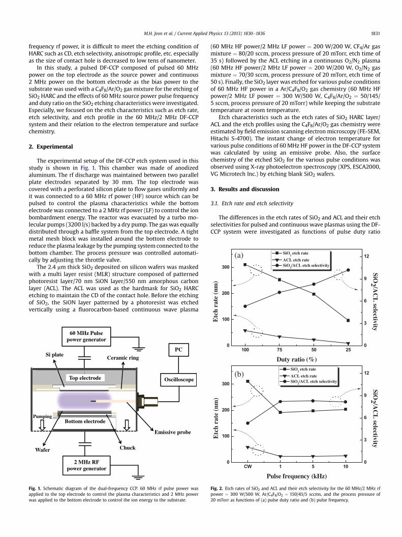
The experimental setup of the DF-CCP etch system used in thisstudy is shown in Fig. 1. This chamber was made of anodizedaluminum. The rf discharge was maintained between two parallelplate electrodes separated by 30 mm. The top electrode wascovered with a perforated silicon plate to flow gases uniformly andit was connected to a 60 MHz rf power (HF) source which can bepulsed to control the plasma characteristics while the bottomelectrode was connected to a 2 MHz rf power (LF) to control the ionbombardment energy. The reactor was evacuated by a turbo mo-lecular pumps (3200 l/s) backed by a dry pump. The gas was equallydistributed through a baffle system from the top electrode. A tightmetal mesh block was installed around the bottom electrode toreduce the plasma leakage by the pumping system connected to thebottom chamber. The process pressure was controlled automati-cally by adjusting the throttle valve.
The 2.4 mm thick SiO2 deposited on silicon wafers was maskedwith a multi layer resist (MLR) structure composed of patternedphotoresist layer/70 nm SiON layer/550 nm amorphous carbonlayer (ACL). The ACL was used as the hardmask for SiO2 HARCetching to maintain the CD of the contact hole. Before the etchingof SiO2, the SiON layer patterned by a photoresist was etchedvertically using a fluorocarbon-based continuous wave plasma
60 MHz Pulse power generator
2 MHz RF power generator
Emissive probe
Si plate Ceramic ring
Top electrode
Bottom electrode
Wafer Chuck
Pumping
Oscilloscope
PC
Fig. 1. Schematic diagram of the dual-frequency CCP. 60 MHz rf pulse power wasapplied to the top electrode to control the plasma characteristics and 2 MHz powerwas applied to the bottom electrode to control the ion energy to the substrate.
(60 MHz HF power/2 MHz LF power ¼ 200 W/200 W, CF4/Ar gasmixture ¼ 80/20 sccm, process pressure of 20 mTorr, etch time of35 s) followed by the ACL etching in a continuous O2/N2 plasma(60 MHz HF power/2 MHz LF power ¼ 200 W/200 W, O2/N2 gasmixture ¼ 70/30 sccm, process pressure of 20 mTorr, etch time of50 s). Finally, the SiO2 layer was etched for various pulse conditionsof 60 MHz HF power in a Ar/C4F8/O2 gas chemistry (60 MHz HFpower/2 MHz LF power ¼ 300 W/500 W, C4F8/Ar/O2 ¼ 50/145/5 sccm, process pressure of 20 mTorr) while keeping the substratetemperature at room temperature.
Etch characteristics such as the etch rates of SiO2 HARC layer/ACL and the etch profiles using the C4F8/Ar/O2 gas chemistry wereestimated by field emission scanning electron microscopy (FE-SEM,Hitachi S-4700). The instant change of electron temperature forvarious pulse conditions of 60 MHz HF power in the DF-CCP systemwas calculated by using an emissive probe. Also, the surfacechemistry of the etched SiO2 for the various pulse conditions wasobserved using X-ray photoelectron spectroscopy (XPS, ESCA2000,VG Microtech Inc.) by etching blank SiO2 wafers.
3. Results and discussion
3.1. Etch rate and etch selectivity
The differences in the etch rates of SiO2 and ACL and their etchselectivities for pulsed and continuous wave plasmas using the DF-CCP system were investigated as functions of pulse duty ratio
CW 1 5 10
0
100
200
300
SiO2 etch rate
ACL etch rateSiO
2/ACL etch selectivity
Pulse frequency (kHz)
Etc
h ra
te (
nm)
0
3
6
9
12
SiO2 /A
CL
selectivity
100 75 50 25
0
100
Duty ratio (%)
Etc
0
3
tivity
(b)
Fig. 2. Etch rates of SiO2 and ACL and their etch selectivity for the 60 MHz/2 MHz rfpower ¼ 300 W/500 W, Ar/C4F8/O2 ¼ 150/45/5 sccms, and the process pressure of20 mTorr as functions of (a) pulse duty ratio and (b) pulse frequency.
M.H. Jeon et al. / Current Applied Physics 13 (2013) 1830e18361832
(100e25% duty) and pulse frequency (CW w10 kHz) of 60 MHz HFsource power and the results are shown in Fig. 2(a) and (b) for thepulse duty ratio and the pulse frequency, respectively. As the SiO2pattern etching condition, 300 W of 60 MHz source power, 500 Wof 2 MHz bias power, 20 mTorr of operating pressure, and 50/145/5 sccm of C4F8/Ar/O2 gas mixture were used. When the pulse dutyratio was varied, the pulse frequency was fixed at 5 kHz and, whenthe pulse frequency was varied, the pulse duty ratio was main-tained at 50%.
As shown in Fig. 2(a), the etch rates of SiO2 and ACL were thehighest for the CW condition (100% duty percentage) and thedecrease of pulse duty ratio decreased the SiO2 etch rate and ACLetch rate almost linearly due to the decrease in the pulse-on timewith the decrease of pulse duty ratio of the 60 MHz HF power.However, as shown in the figure, the etch selectivity of SiO2 overACL increased almost linearly with the decrease of pulse duty ratio.On the other hand, when the pulse frequency was varied whilekeeping the pulse duty ratio at 50%, the etch rates of SiO2 and ACLwere not changed significantly with pulse frequency even thoughthe change from CW to pulse condition decreased the etch rates ofSiO2 and ACL and increased the etch selectivity. To investigate thedifferences in the etch characteristics on the pulse duty ratio andthe pulse frequency, the chemistry of fluorocarbon polymer residueremaining on the etched SiO2 surface and the instant variationof electron temperature for different pulsing conditions wereinvestigated.
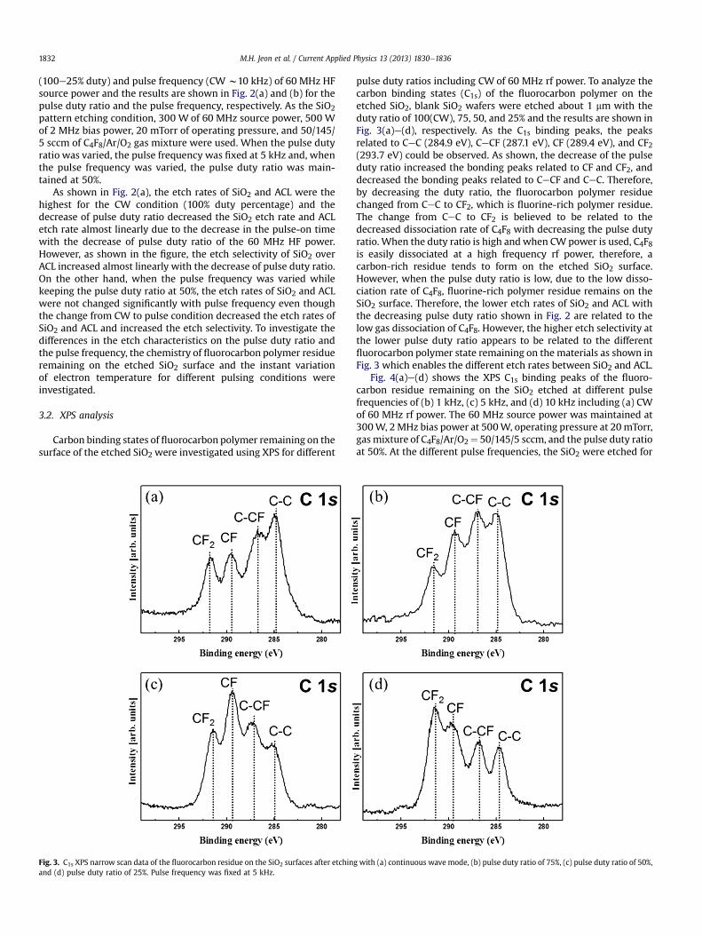
3.2. XPS analysis
Carbon binding states of fluorocarbon polymer remaining on thesurface of the etched SiO2 were investigated using XPS for different
Fig. 3. C1s XPS narrow scan data of the fluorocarbon residue on the SiO2 surfaces after etchinand (d) pulse duty ratio of 25%. Pulse frequency was fixed at 5 kHz.
pulse duty ratios including CW of 60 MHz rf power. To analyze thecarbon binding states (C1s) of the fluorocarbon polymer on theetched SiO2, blank SiO2 wafers were etched about 1 mm with theduty ratio of 100(CW), 75, 50, and 25% and the results are shown inFig. 3(a)e(d), respectively. As the C1s binding peaks, the peaksrelated to CeC (284.9 eV), CeCF (287.1 eV), CF (289.4 eV), and CF2(293.7 eV) could be observed. As shown, the decrease of the pulseduty ratio increased the bonding peaks related to CF and CF2, anddecreased the bonding peaks related to CeCF and CeC. Therefore,by decreasing the duty ratio, the fluorocarbon polymer residuechanged from CeC to CF2, which is fluorine-rich polymer residue.The change from CeC to CF2 is believed to be related to thedecreased dissociation rate of C4F8 with decreasing the pulse dutyratio. When the duty ratio is high and when CW power is used, C4F8is easily dissociated at a high frequency rf power, therefore, acarbon-rich residue tends to form on the etched SiO2 surface.However, when the pulse duty ratio is low, due to the low disso-ciation rate of C4F8, fluorine-rich polymer residue remains on theSiO2 surface. Therefore, the lower etch rates of SiO2 and ACL withthe decreasing pulse duty ratio shown in Fig. 2 are related to thelow gas dissociation of C4F8. However, the higher etch selectivity atthe lower pulse duty ratio appears to be related to the differentfluorocarbon polymer state remaining on the materials as shown inFig. 3 which enables the different etch rates between SiO2 and ACL.
Fig. 4(a)e(d) shows the XPS C1s binding peaks of the fluoro-carbon residue remaining on the SiO2 etched at different pulsefrequencies of (b) 1 kHz, (c) 5 kHz, and (d) 10 kHz including (a) CWof 60 MHz rf power. The 60 MHz source power was maintained at300W, 2MHz bias power at 500W, operating pressure at 20mTorr,gasmixture of C4F8/Ar/O2¼ 50/145/5 sccm, and the pulse duty ratioat 50%. At the different pulse frequencies, the SiO2 were etched for
g with (a) continuous wave mode, (b) pulse duty ratio of 75%, (c) pulse duty ratio of 50%,

Fig. 4. C1s XPS narrow scan data of the fluorocarbon residue on the SiO2 surfaces after etching with (a) continuous wave mode, (b) pulse frequency of 1 kHz, (c) pulse frequency of5 kHz, and (d) the pulse frequency of 10 kHz. Pulse duty ratio was fixed at 50%.
M.H. Jeon et al. / Current Applied Physics 13 (2013) 1830e1836 1833
3 min. Compared to the CW plasma, when SiO2 was etched bypulsed plasmas, the XPS C1s peak showed higher binding peaksrelated to CF and CF2. However, as shown in the figures, the vari-ation of the pulse frequency from 1 to 10 kHz did not change the C1s
binding peaks of the fluorocarbon polymer residue, indicatingsimilar gas dissociation characteristics. The XPS results wereconsistent with the results of etch rates and etch selectivitiesmeasured as a function of pulse frequency in Fig. 2(b). The gas
0020010
0
4
8
12
Ele
ctro
n te
mpe
ratu
re (
eV)
Time (µs)
Continuous wave plasmaDR 75 %, Freq. 5 kHzDR 50 %, Freq. 5 kHzDR 25 %, Freq. 5 kHz
Fig. 5. Instant variation of electron temperature estimated as a function of time for thepulse duty ratio of 100(CW), 75, 50, and 25% at the pulse frequency of 5 kHz. The60 MHz source power was maintained at 300 W with 150 sccm Ar and at operatingpressure of 20 mTorr. No 2 MHz bias power was applied to the substrate.
dissociation characteristics in the pulsed plasmas are related to thevariation of the plasma characteristics. Therefore, in this study, asone of the important plasma characteristics, the variation of elec-tron temperature in the pulsed plasmas was measured using anemissive probe.
3.3. Electron temperature
When electrons in the plasma haveMaxwellian distribution, theelectron temperature can be used as the change of electron energydistribution which is related to the gas dissociation characteristics.Due to the deposition characteristics of C4F8, and, due to the noiseproblem under the pulsing conditions, instead of a typical Lang-muir probe, an emissive probe and Ar gas were used and thecharacteristics of the plasmas were estimated. By heating andfloating the probe tip of the emissive probe, instant plasma po-tential (Vp) and instant floating potential (Vf) during the operationof the pulsed plasma can be measured, respectively, and the instantelectron temperature can be estimated using the followingformula;
Vp � Vf ¼ kTe2e
ln�2Mpm
�
where, k is Boltzmann constant, Te is electron temperature,m is theelectron mass, and M is the atomic mass of the discharge gas [19].Therefore, using the emissive probe, the effects of rf pulse duty ratioand rf pulse frequency on the change of instant electron tempera-ture were estimated and the results are shown in Figs. 5 and 6,respectively.
Fig. 5 shows the instant change of electron temperaturemeasured as a function of time for the pulse duty ratio of 100(CW),

0 250 500 750 10000
5
10
15
Ele
ctro
n te
mpe
ratu
re (
eV)
Time (µs)
Freq. 1 kHz, DR 50 %Freq. 5 kHz, DR 50 %Freq. 10 kHz, DR 50 %
Fig. 6. Instant variation of electron temperature estimated as a function of time for thepulse frequencies of 1, 5, and 10 kHz and at the pulse duty ratio of 50%. Other con-ditions were maintained same as those in Fig. 5.
M.H. Jeon et al. / Current Applied Physics 13 (2013) 1830e18361834
75, 50, and 25% and at the pulse frequency of 5 kHz. The 60 MHzsource power was maintained at 300 W with 150 sccm Ar andoperating pressure of 20 mTorr. No 2 MHz bias power was appliedto the substrate. As shown in Fig. 5, for the continuous wave Arplasma, the electron temperature was measured at about 8.1 eV.
Fig. 7. SiO2 HARC hole etch profiles observed by FE-SEM after the etching at different pulseduty ratio was 50% and the etch time was maintained for 3 min. Other etch conditions are
However, as shown in the figure, the decrease of the pulse dutyratio decreased the average electron temperature even thoughtherewas an overshoot of instant electron temperature at the initialpulse-on time. Even though the experimentwas carried outwith anAr plasma, it is believed that the similar variation of electrontemperature can be obtained with reactive fluorocarbon gases suchas C4F8. Therefore, a lower average electron temperature obtainedwith decreasing pulse duty ratio will decrease the dissociation ofthe fluorocarbon gas in addition to the increased recombination ofgas species during the pulse-off time, and which will increase thepolymerization on the etched material surface by increasing CxFyradical density and decreasing F density in the plasma. Therefore,the higher CF2 binding of the fluorocarbon residue on the SiO2etched with the lower pulse duty percentage shown in Fig. 3 isbelieved to be related to the decreased dissociation of C4F8 gas bydecreasing the average electron temperature.
Fig. 6 shows the instant variation of electron temperaturemeasured as a function of time for the pulse frequency of 1, 5, and10 kHz and at the pulse duty ratio of 50%. Other conditions weremaintained same as those in Fig. 5. As shown in the figure, eventhough the pulse frequency was varied, the instant electron tem-perature during the pulse-on time was similar at 7e7.5 eV and,after the pulse-off, the electron temperature was rapidly decreasedclose to 0. Therefore, the average electron temperature was alsosimilar for the pulse frequencies investigated, and which maysuggest no significant variation in the dissociation characteristics offluorocarbon gas for our experimental conditions. No significant
frequencies of (b) 1 kHz, (c) 5 kHz, and (d) 10 kHz including (a) CW plasma. The pulsethe same as those in Fig. 2(b).
M.H. Jeon et al. / Current Applied Physics 13 (2013) 1830e1836 1835
change in the etch rates of SiO2 and ACL and their etch selectivitiesobserved as a function of pulse frequency in our experiment ap-pears to be related to the no significant variation of the fluoro-carbon gas dissociation in the plasma.
3.4. Etch profile
Fig. 7(a)e(d) shows the SiO2 HARC etch profile observed by SEMafter the etching at different pulse frequencies of (b) 1 kHz, (c) 5 kHz,and (d) 10 kHz including (a) CW plasma. The pulse duty ratio was50% and the etch time was maintained for 3 min. Other etch con-ditions were the same as those in Fig. 2(b). As shown in Fig. 7(a),when SiO2 contact hole was etched using a CWplasma, even thoughthe etch depths of SiO2 are higher than those etched by pulsedplasmas, the etch selectivity over ACL was lower and, due to thedifficulty in forming sidewall passivation during the etching of SiO2
contact hole, the SiO2 contact hole size was increased significantlyafter the etching. However, by using the pulsed plasmas, due to theformation of CxFy radicals in the plasma and due to the formation of
Fig. 8. SiO2 contact hole etch profiles observed by FE-SEM after the etching of SiO2 patterkeeping the pulse frequency at 5 kHz. The etch time was varied to obtain about 1 mm of SiO
a fluorocarbon residue having more CFx (x ¼ 1e2) binding on thesurface, not only the etch selectivity but also the contact hole sizeand etch profile were improved due to the formation of enoughsidewall passivation during the etching even though the SiO2 etchrates are lower than that etched using a CW plasma. However, theSiO2 contact hole etch characteristics measured as a function ofpulse frequency from 1 to 10 kHz such as etch depth of SiO2 contacthole, the contact hole size, etch profile, etc. were similar each otheras expected from the results in Figs. 2(b), 4 and 6. It is known that,the SiO2 contact hole etch profile is easily distorted due to thecharging of the contact hole during the etching. In our pulsedplasmas, the 60 MHz power is pulsed and the 2 MHz rf powerapplied to the substrate is stayed on during the pulse-off period.Therefore, the bias voltage to the substrate is increased during thepulse-off period and it can improve the SiO2 contact etch profile byincreasing the directionality of the incident ion by increasing the ionbombardment energy to the substrate during the pulse-off period.
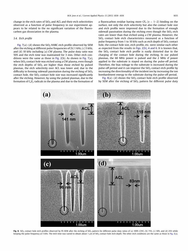
Fig. 8(a)e(d) shows the SiO2 contact hole etch profile observedby SEM after the etching of SiO2 pattern for different pulse duty
n for different pulse duty ratios of (a) 100% (CW), (b) 75%, (c) 50%, and (d) 25% while2 contact hole etch depth. The other etch conditions are the same as those in Fig. 2(a).

M.H. Jeon et al. / Current Applied Physics 13 (2013) 1830e18361836
ratios of (a) 100% (CW), (b) 75%, (c) 50%, and (d) 25% while keepingthe pulse frequency at 5 kHz. The etch time was varied to obtainabout 1 mm of SiO2 contact hole etch depth. The other etch condi-tions are the same as those in Fig. 2(a). As shown in the figure, asthe pulse duty ratio is decreased from 100% to 25%, the ACL etchrate was decreased and the contact hole size was decreased close tothat of ACL mask. The improvement of SiO2 etch selectivity to ACLand the improvement of contact hole size at the lower pulse dutyratio is believed to be related to the formation of a CFx-rich (x ¼ 1e2) fluorocarbon polymer residue on the surface by the decreasedgas dissociation of C4F8 gas at the lower average electron energywith the increase of the pulse-off time. In addition, as shown in thefigure, the bottom etch profile of SiO2 contact hole was improvedmore with the decrease of duty ratio possibly due to the moredirectional reactive ions due to the increased pulse-off time at thelower pulse duty ratio. However, the use of lower duty ratio ofpulsed plasma such as 25% of duty ratio increases the etch time toform a deep SiO2 contact hole, therefore, too low duty ratio may notbe applicable in the actual SiO2 contact hole etch processing.
4. Conclusions
In this study, 60 MHz/2 MHz DF-CCP, where 60 MHz rf powerwas applied to the top electrode and 2MHz rf power was applied tothe substrate, was used in the etching of SiO2 HARC and the effects60 MHz rf pulsing such as pulse frequency and pulse duty ratio onthe SiO2 etch characteristics have been investigated using C4F8-based gas mixtures. The application of 60 MHz rf power pulsingdecreased the etch rate of SiO2, however, it improved the etchselectivity of SiO2 over ACL and also improved the SiO2 contact etchprofile and contact hole size. The decrease of pulse duty ratio of60 MHz rf power further improved the etch selectivity, the contactetch profile, and the contact hole CD further while decreasing theSiO2 etch rate, however, the variation of pulse duty frequency at afixed pulse duty ratio did not change the etch characteristicssignificantly. XPS C1s narrow scan data of the fluorocarbon polymerlayer on the etched SiO2 surface showed that the decrease of pulseduty ratio increased the binding peaks related to CF1 and CF2bindings, therefore, a CFx-rich fluorocarbon polymerwas formed onthe SiO2 surface during the etching indicating the lower dissocia-tion of C4F8 for the decreased pulse duty ratio. The lower dissoci-ation of C4F8 for the decreased pulse duty ratio was caused bydecreased average electron temperature at the lower pulse dutyratio. However, when the pulse frequency was varied at a fixed duty
ratio, the XPS C1s data showed that carbon binding characteristicsof the fluorocarbon residue were not changed significantly due tono significant change in the electron temperature characteristicswith the pulse frequency at a fixed pulse duty ratio. The improve-ment of the SiO2 contact etch profile with the decrease of pulseduty ratio was also related to more directional reactive ions due tothe increased pulse-off time at the lower pulse duty ratio. Eventhough low pulse duty ratios improves many important etchcharacteristics, due to the decrease of SiO2 etch rate, careful studymay be required before it is applied to SiO2 contact hole etchprocessing.
Acknowledgments
This work was supported by the Industrial Strategic technologydevelopment program (10041926, Development of high densityplasma technologies for thin film deposition of nanoscale semi-conductor and flexible display processing) funded by the Ministryof Knowledge Economy (MKE, Korea) and the World Class Univer-sity program of the National Research Foundation of Korea (GrantNo. R32-10124) and also by SEMES.
References
[1] D. Koehler, D. Fischer, ECS Trans. 138 (2008) 47.[2] T.F. Yen, K.J. Chang, K.-F. Chiu, Microelectron. Eng. 82 (2005) 129.[3] J.-K. Lee, I.-Y. Jang, S.-H. Lee, C.-K. Kim, S.H. Moon, J. Electrochem. Soc. 156
(2009) D269.[4] K. Hashimoto, Jpn. J. Appl. Phys. 32 (1993) 6109.[5] K. Eriguchi, K. Ono, J. Phys. D 41 (2008) 024002.[6] Seiji Samukawa, Jpn. J. Appl. Phys. 33 (1994) 2133.[7] I.G. Kim, N.S. Kim, J.S. Park, D.Y. Park, Jpn. J. Appl. Phys. 41 (2002) 2380.[8] H. Ohtake, S. Samukawa, J. Vac. Sci. Technol. B 20 (2002) 1026.[9] H. Ohtake, B. Jinnai, Y. Suzuki, S. . Soda, T. Shimmura, S. Samukawa, J. Vac. Sci.
Technol. A 24 (2006) 2172.[10] C.J. Choi, O.S. Kwon, Y.S. Seol, Jpn. J. Appl. Phys. 37 (1998) 6894.[11] Y. Ichihashi, Y. Ishikawa, R. Shimizu, S. Samukawa, J. Vac. Sci. Technol. B 28
(2010) 577.[12] T. Ohmori, T.K. Goto, T. Kitajima, T. Makabe, Appl. Phys. Lett. 83 (2003) 4637.[13] T. Kitajima, Y. Takeo, Z.L. .Petrovic, T. Makabe, Appl. Phys. Lett. 77 (2000) 489.[14] K. Bera, S. Rauf, A. Balakrishna, K. Collins, IEEE Trans. Plasma Sci. 38
(2010) 3241.[15] T. Kitamura, N. Nakano, T. Makabe, Y. Yamaguchi, Plasma Sources Sci. Technol.
2 (1993) 40.[16] Y. Yang, Mark J. Kushner, J. Appl. Phys. 108 (2010) 113306.[17] M.A. Lieberman, J.P. Booth, P. Chabert, J.M. Rax, M.M. Turner, Plasma Sources
Sci. Technol. 11 (2002) 283.[18] A. Agarwal, S. Rauf, K. Collins, Appl. Phys. Lett. 99 (2011) 021501.[19] A. Mishra, M.H. Jeon, K.N. Kim, G.Y. Yeom, Plasma Sources Sci. Technol. 21
(2012) 055006.