
Chapter 4 In silico design optimization of nanowire...
41
75 Chapter 4 In silico design optimization of nanowire circuits 4.1 Introduction The continued miniaturization of semiconductor transistors has several associated scientific and engineering challenges. High-κ dielectric/metal gate MOSFETs, strained- Si channel devices, and non-planar (tri-gate or Fin FET) structures are most likely to be the next-generation technologies. 1 Further into the future, more novel transistor-channel options are being explored, including III-V compound semiconductors, 2–4 semiconductor nanowires (NWs), 5–8 and carbon nanotubes (CNTs). 9–15 NWs and CNTs are not prepared using conventional lithography, implying that NW or CNT-based devices can be scaled to very high device densities. Small circuits, such as inverters, 6, 9–14 basic logic gates, 5, 13, 14, 16 and ring oscillators, 13, 14, 17 have already been demonstrated using NW and CNT field-effect transistors (FETs). However, few demonstrations have provided realistic competition to current CMOS technology. This is
Transcript of Chapter 4 In silico design optimization of nanowire...
75
Chapter 4
In silico design optimization of nanowire circuits
4.1 Introduction
The continued miniaturization of semiconductor transistors has several associated
scientific and engineering challenges. High-κ dielectric/metal gate MOSFETs, strained-
Si channel devices, and non-planar (tri-gate or Fin FET) structures are most likely to be
the next-generation technologies.1 Further into the future, more novel transistor-channel
options are being explored, including III-V compound semiconductors,2–4 semiconductor
nanowires (NWs),5–8 and carbon nanotubes (CNTs).9–15
NWs and CNTs are not prepared using conventional lithography, implying that
NW or CNT-based devices can be scaled to very high device densities. Small circuits,
such as inverters,6, 9–14 basic logic gates,5, 13, 14, 16 and ring oscillators,13, 14, 17 have already
been demonstrated using NW and CNT field-effect transistors (FETs). However, few
demonstrations have provided realistic competition to current CMOS technology. This is
76 largely because constructing even simple prototype circuits from these materials is a
daunting challenge.
Computer-aided design (CAD) tools can increase the efficiency of electronic
circuit design and optimization by yielding insights into circuit performance, which in
turn provide design feedback, resulting in optimized fabricated circuits. While NW and
CNT devices have been modeled in a circuit simulation environment,18–20 these efforts
have been largely independent of the fabrication and materials aspects of these
nanocircuits. Adding CAD into the design process will result the more efficient design of
high performance nano-ICs.
Therefore, a methodology was developed that couples circuit simulations and
fabricated prototype devices into the design process of the nanowire logic circuits.21 A
CS inverter, or NOT gate, was chosen for optimization because it is conceptually easy to
understand while also yielding several performance metrics for CMOS logic. CS
inverters require both a p- and n-type FET, arranged so that an input logic voltage signal
will turn one FET “on” and other “off”. This architecture prevents the voltage that
powers the circuit from having a direct pathway to ground, which makes the circuit
energy efficient.8 However, such circuits are difficult to fabricate from most NWs or
CNTs, because assembling different types of NWs or NTs from well-defined electronic
circuits remains a significant challenge. The superlattice nanowire pattern transfer
(SNAP) technique22 eliminates this problem and has been used to successfully fabricate
high-performance devices7 and circuits8 (see Chapters 2 and 3). Si NWs have the
additional benefit of being a highly studied material and are compatible with existing Si
processing technologies, making them a realistic choice for nanoelectronics circuits.
77
From candidate Si NW p- and n-FET devices, current-voltage (I-V), conductance-
voltage (G-V), and capacitance-voltage (C-V) measurements were tabulated and
introduced into a circuit simulator. DC and transient analyses were carried out to
investigate and optimize, in silico, a variety of circuit metrics, with a focus on optimizing
the gain. Other metrics that could be readily simulated include the input and supply
voltage levels, propagation delays, leakage currents, parasitic resistances and
capacitances, and power consumption. Next, the results of these simulations were fed
back into the nanofabrication procedures to produce a CS inverter with an optimized gain
of 45. This represents a more than 5-fold improvement over the initially fabricated
prototype circuit from which the basis set of measurements were extracted.
4.1.1 Organization of the chapter
In this chapter, the fabrication and characterization of the candidate NW FETs are
described, followed by a description of the simulation methods and the results of the DC
and transient computational analyses. Finally, the simulated results were verified
experimentally and high-performance inverters that are competitive, in terms of their
gain, with CMOS are demonstrated.
78 4.2 Large-area nanowire transistors
Special NW FETs were specifically designed for this project that had a large area
channel region. This design ensured that high-quality capacitance data could be obtained
from these prototype devices. A transistor’s gate capacitance can be approximated by a
parallel-plate capacitor, which has a capacitance of:
dAKC oε= .
(4.1)
Here, A is the area of the plate, d is the distance between the plates, K is the dielectric
constant of the oxide material, and εo is the permittivity of free space. A typical NW FET
channel dimensions are 100 × 500 nm and the gate oxide thickness is ~ 10 nm.
Assuming a dielectric constant of ~ 3.7, the gate capacitance of the device would be ~ 0.1
fF. This capacitance is too small to accurately measure using conventional equipment,23
so large area devices were designed with channel widths of 12 µm and channel lengths of
9–11 µm. This increased the expected gate capacitance to 0.3 pF, which could be easily
measured.
4.2.1 Fabrication of large-area nanowire transistors
Fabrication of the large-area transistors (Figure 4.1A) was similar to the
fabrication of standard-size transistors (see Section 2.2). Si NW devices were fabricated
on SIMOX-SOI wafers (34 nm <100> Si on 250 nm Si oxide) (Simgui, Shanghai, China).
Substrates were cleaned using the standard RCA process and then doped either n- or p-
type by applying a spin-on dopant (SOD) and annealing using rapid thermal processing
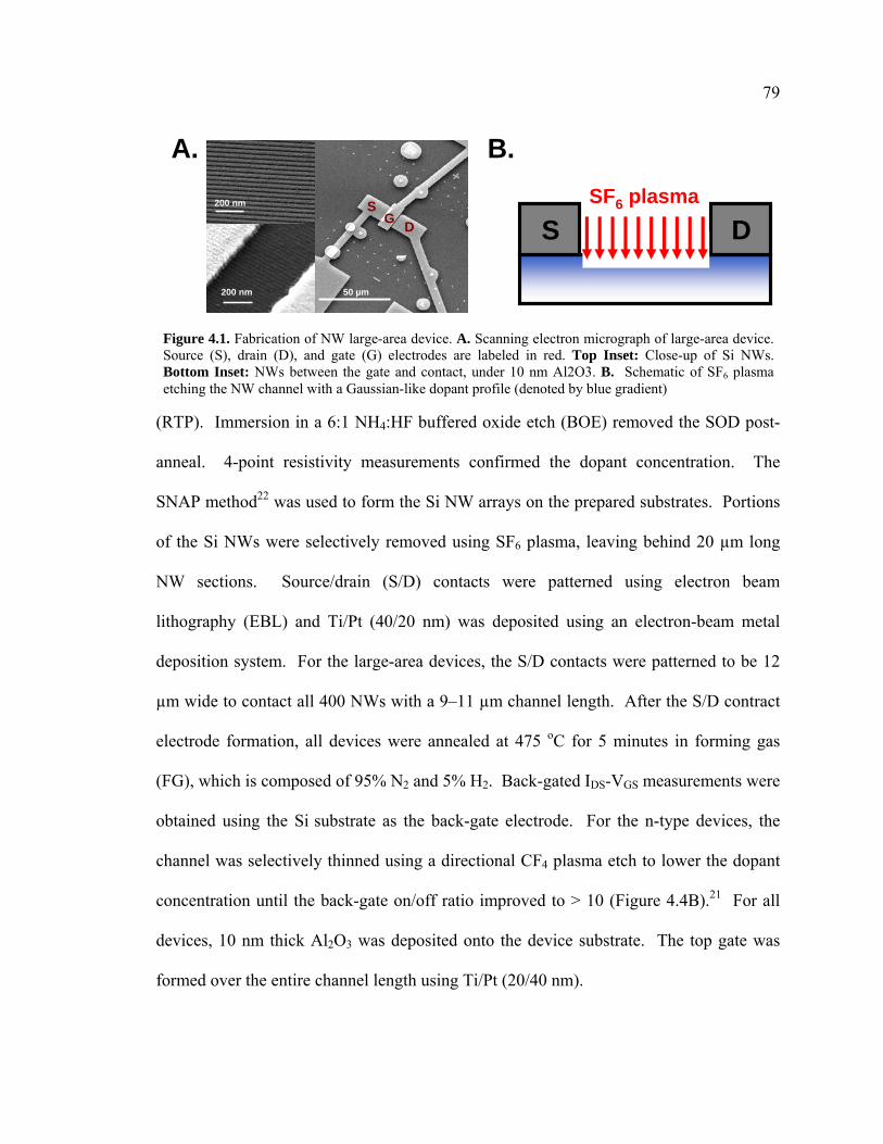
79
(RTP). Immersion in a 6:1 NH4:HF buffered oxide etch (BOE) removed the SOD post-
anneal. 4-point resistivity measurements confirmed the dopant concentration. The
SNAP method22 was used to form the Si NW arrays on the prepared substrates. Portions
of the Si NWs were selectively removed using SF6 plasma, leaving behind 20 µm long
NW sections. Source/drain (S/D) contacts were patterned using electron beam
lithography (EBL) and Ti/Pt (40/20 nm) was deposited using an electron-beam metal
deposition system. For the large-area devices, the S/D contacts were patterned to be 12
µm wide to contact all 400 NWs with a 9–11 µm channel length. After the S/D contract
electrode formation, all devices were annealed at 475 oC for 5 minutes in forming gas
(FG), which is composed of 95% N2 and 5% H2. Back-gated IDS-VGS measurements were
obtained using the Si substrate as the back-gate electrode. For the n-type devices, the
channel was selectively thinned using a directional CF4 plasma etch to lower the dopant
concentration until the back-gate on/off ratio improved to > 10 (Figure 4.4B).21 For all
devices, 10 nm thick Al2O3 was deposited onto the device substrate. The top gate was
formed over the entire channel length using Ti/Pt (20/40 nm).
S DSF6 plasma
B.
200 nm
200 nm
50 µm
S D G
A.
Figure 4.1. Fabrication of NW large-area device. A. Scanning electron micrograph of large-area device. Source (S), drain (D), and gate (G) electrodes are labeled in red. Top Inset: Close-up of Si NWs. Bottom Inset: NWs between the gate and contact, under 10 nm Al2O3. B. Schematic of SF6 plasma etching the NW channel with a Gaussian-like dopant profile (denoted by blue gradient)
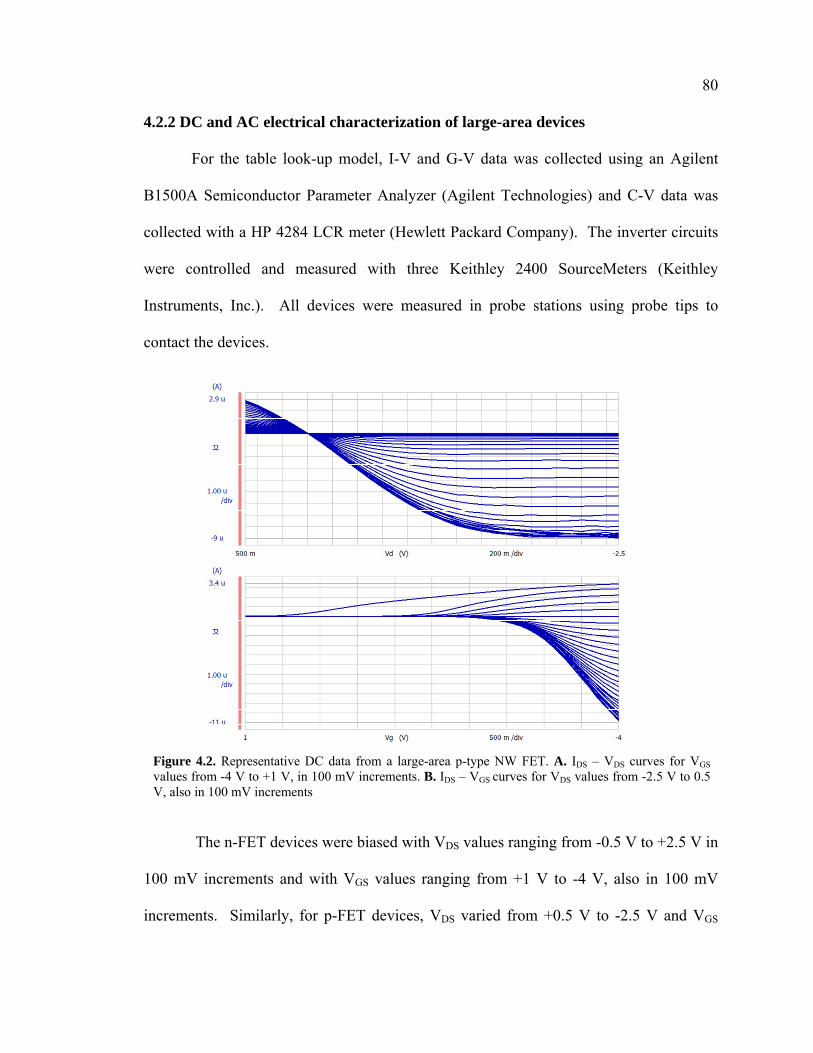
80 4.2.2 DC and AC electrical characterization of large-area devices
For the table look-up model, I-V and G-V data was collected using an Agilent
B1500A Semiconductor Parameter Analyzer (Agilent Technologies) and C-V data was
collected with a HP 4284 LCR meter (Hewlett Packard Company). The inverter circuits
were controlled and measured with three Keithley 2400 SourceMeters (Keithley
Instruments, Inc.). All devices were measured in probe stations using probe tips to
contact the devices.
The n-FET devices were biased with VDS values ranging from -0.5 V to +2.5 V in
100 mV increments and with VGS values ranging from +1 V to -4 V, also in 100 mV
increments. Similarly, for p-FET devices, VDS varied from +0.5 V to -2.5 V and VGS
Figure 4.2. Representative DC data from a large-area p-type NW FET. A. IDS – VDS curves for VGS values from -4 V to +1 V, in 100 mV increments. B. IDS – VGS
curves for VDS values from -2.5 V to 0.5 V, also in 100 mV increments
81 varied from +1V to -4V (see Figure 4.2). Both IDS and IGS were measured for both sets of
devices. Transconductance, gm, and channel conductance, gd, for every VGS and VDS
value were calculated automatically by the Semiconductor Parameter Analyzer. The
transconductance is defined as:24
.constVD
Dm
GVIg
=∂∂
≡ (4.2)
and the channel conductance is defined as:24
.constVG
Dd
DVIg
=∂∂
≡ . (4.3)
To obtain good gm and gd values, the voltage increments were kept very small.
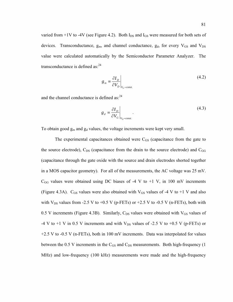
The experimental capacitances obtained were CGS (capacitance from the gate to
the source electrode), CDS (capacitance from the drain to the source electrode) and CGG
(capacitance through the gate oxide with the source and drain electrodes shorted together
in a MOS capacitor geometry). For all of the measurements, the AC voltage was 25 mV.
CGG values were obtained using DC biases of -4 V to +1 V, in 100 mV increments
(Figure 4.3A). CGS values were also obtained with VGS values of -4 V to +1 V and also
with VDS values from -2.5 V to +0.5 V (p-FETs) or +2.5 V to -0.5 V (n-FETs), both with
0.5 V increments (Figure 4.3B). Similarly, CDS values were obtained with VGS values of
-4 V to +1 V in 0.5 V increments and with VDS values of -2.5 V to +0.5 V (p-FETs) or
+2.5 V to -0.5 V (n-FETs), both in 100 mV increments. Data was interpolated for values
between the 0.5 V increments in the CGS and CDS measurements. Both high-frequency (1
MHz) and low-frequency (100 kHz) measurements were made and the high-frequency
82 measurements were used in the look-up-table model. Data taken below 100 kHz was
very noisy and unusable.
In addition to measuring the capacitance of the large-area FETs, metal capacitors
containing 10 nm of deposited Al2O3 were fabricated with several different device areas
to directly measure the dielectric constant of the dielectric layer. Assuming a dielectric
thickness of 10 nm (as determined by the electron deposition chamber quartz crystal
oscillator) and using equation 4.1, the average dielectric constant measured was 3.68.
This value is significantly lower than the dielectric constant of high-quality Al2O3, ~ 10,
and signifies the presence of defects in the film due to poor deposition control.
4.2.3 Calculation of performance metrics
For the fabricated test structures, the threshold voltage was calculated from the
IDS-VGS plots. Since these devices do not have the conventional MOSFET structure in
which the channel conduction arises from an inversion layer (Figure 4.4A), the definition
of threshold voltage (VT) will be clarified. The NW devices have a similar structure to
-4 -2 0 20.1
0.2
0.3
0.4
DC Voltage (V)
Cap
acita
nce
(pF)
-4 -3 -2 -1 0 1
0.01
0.02
0.03
0.04
0.05
0.06
0.07
VGS (V)
Cap
acita
nce
(pF)
B.A.
-4 -2 0 20.1
0.2
0.3
0.4
DC Voltage (V)
Cap
acita
nce
(pF)
-4 -3 -2 -1 0 1
0.01
0.02
0.03
0.04
0.05
0.06
0.07
VGS (V)
Cap
acita
nce
(pF)
B.A.
Figure 4.3. Representative capacitance data of NW FET devices. A. CGG versus VGG at 1 MHz (solid blue curve) and 100 kHz (dotted green curve). B. CGS versus VGS for various VDS values
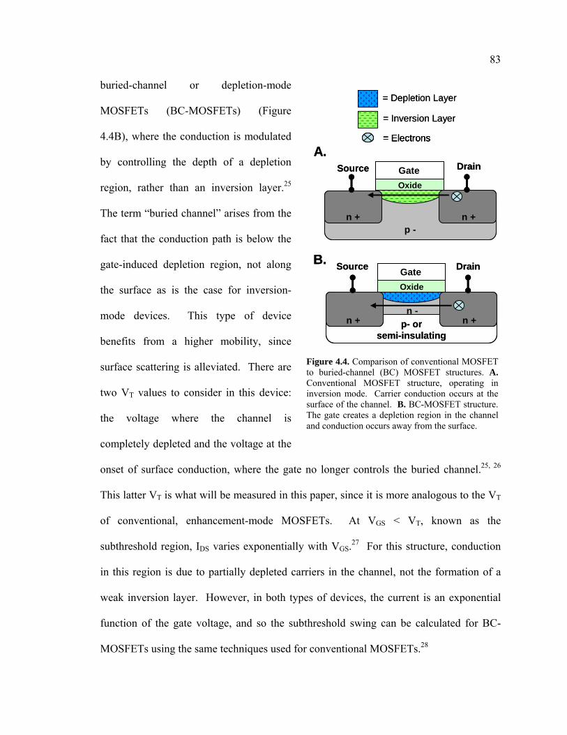
83 buried-channel or depletion-mode
MOSFETs (BC-MOSFETs) (Figure
4.4B), where the conduction is modulated
by controlling the depth of a depletion
region, rather than an inversion layer.25
The term “buried channel” arises from the
fact that the conduction path is below the
gate-induced depletion region, not along
the surface as is the case for inversion-
mode devices. This type of device
benefits from a higher mobility, since
surface scattering is alleviated. There are
two VT values to consider in this device:
the voltage where the channel is
completely depleted and the voltage at the
onset of surface conduction, where the gate no longer controls the buried channel.25, 26
This latter VT is what will be measured in this paper, since it is more analogous to the VT
of conventional, enhancement-mode MOSFETs. At VGS < VT, known as the
subthreshold region, IDS varies exponentially with VGS.27 For this structure, conduction
in this region is due to partially depleted carriers in the channel, not the formation of a
weak inversion layer. However, in both types of devices, the current is an exponential
function of the gate voltage, and so the subthreshold swing can be calculated for BC-
MOSFETs using the same techniques used for conventional MOSFETs.28
p- or semi-insulating
OxideGateSource Drain
n + n +n -
= Depletion Layer
= Inversion Layer
= Electrons
p -
Source Drain
n + n +
OxideGate
A.
B.
p- or semi-insulating
OxideGateGateSource Drain
n + n +n -
= Depletion Layer
= Inversion Layer
= Electrons= Electrons
p -
Source Drain
n + n +
OxideGateGate
A.
B.
Figure 4.4. Comparison of conventional MOSFET to buried-channel (BC) MOSFET structures. A. Conventional MOSFET structure, operating in inversion mode. Carrier conduction occurs at the surface of the channel. B. BC-MOSFET structure. The gate creates a depletion region in the channel and conduction occurs away from the surface.
84
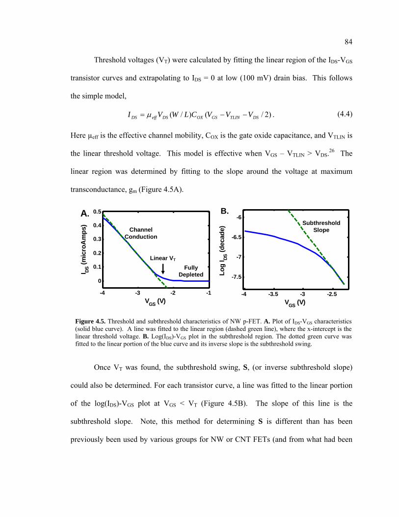
Threshold voltages (VT) were calculated by fitting the linear region of the IDS-VGS
transistor curves and extrapolating to IDS = 0 at low (100 mV) drain bias. This follows
the simple model,
)2/()/( DSTLINGSOXDSeffDS VVVCLWVI −−= μ . (4.4)
Here µeff is the effective channel mobility, COX is the gate oxide capacitance, and VTLIN is
the linear threshold voltage. This model is effective when VGS – VTLIN > VDS.26 The
linear region was determined by fitting to the slope around the voltage at maximum
transconductance, gm (Figure 4.5A).
Once VT was found, the subthreshold swing, S, (or inverse subthreshold slope)
could also be determined. For each transistor curve, a line was fitted to the linear portion
of the log(IDS)-VGS plot at VGS < VT (Figure 4.5B). The slope of this line is the
subthreshold slope. Note, this method for determining S is different than has been
previously been used by various groups for NW or CNT FETs (and from what had been
-4 -3 -2 -1
0
0.1
0.2
0.3
0.4
0.5
VGS (V)
I DS (m
icro
Am
ps)
Linear VT
Channel Conduction
FullyDepleted
A.
-4 -3.5 -3 -2.5
-7.5
-7
-6.5
-6
VGS (V)
Log
I DS (d
ecad
e)Subthreshold
Slope
B.
Figure 4.5. Threshold and subthreshold characteristics of NW p-FET. A. Plot of IDS-VGS characteristics (solid blue curve). A line was fitted to the linear region (dashed green line), where the x-intercept is the linear threshold voltage. B. Log(IDS)-VGS plot in the subthreshold region. The dotted green curve was fitted to the linear portion of the blue curve and its inverse slope is the subthreshold swing.
85 described in Chapter 2),7, 15, 29 but yields results that are more comparable to standard
MOSFET parameters.
For the n-type NW FET, the threshold voltage was calculated to be -0.9 V. The
subthreshold swing was calculated to be ~ 550 mV/dec. For the p-type NW FET, the
threshold voltage was determined to be -2.3 V and S was ~ 450 mV/dec. For BC-
MOSFETs, the ideal value for S is > 80 mV/dec (for inversion-type MOSFETS, the ideal
is 60 mV/dec) and as the channel thickness increases relative to the substrate, S becomes
> 100 mV/dec. In these NW devices, there is no substrate junction to help modulate a
depletion region so the gate alone must be as effective as possible. Since the gate only
modulates the top of the NWs, this leads to a increase in S.30 Other issues, such as the
effect of surface states on a large surface-area-to-volume ratio device and the thick (and
low-quality) dielectric material also lead to a degradation of S. However, these devices
still show excellent electrical properties, such as a high on/off ratio (approximately 104
for both p- and n-FETs) and high on-currents (p-type: ~ 1 µA; n-type ~ 5 µA).
4.3 Setup of device look-up table model and simulations
Device look-up table-models are not new—they have been implemented using
several simulators, including SPICE.31–34 However, tabular models are typically
employed to decrease the circuit simulation evaluation time and are usually constructed
using analytical device models, supplemented with experimental data only partially, if at
86 all. Analytical models are computationally time-consuming to implement during a circuit
simulation if the device model becomes very complex. As devices continue to shrink and
exhibit non-bulk effects, such as performance degradation due to surface-states, their
associated analytical models become increasingly complex and more difficult to
develop.32 Therefore, tabular models become an attractive alternative.
There are two caveats to using an experimentally derived table model. The first is
that all device parameters (channel length, dopant profile, source/drain/gate materials,
temperature, etc.) are fixed for a given model and cannot be altered in the circuit
simulation environment. Second, not every conductance and capacitance value can be
directly measured for input into the look-up table. The approximations that were used for
the look-up table are described below.
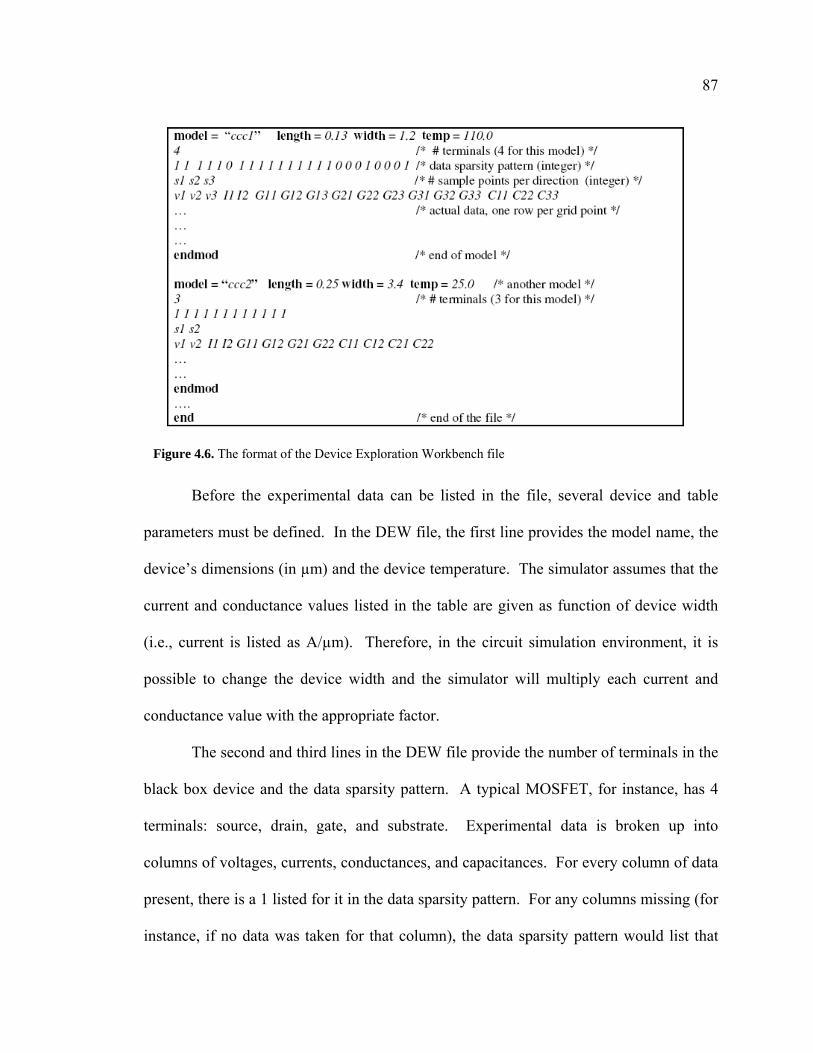
4.3.1 The look-up-table format
The device look-up table, labeled the Device Exploration Workbench (DEW) in
the Intel simulation environment, is used to define an n-terminal black box device that
can be used as a circuit component in the circuit simulator. The file format is shown in
Figure 4.6. An example DEW file appears in Appendix A. Essentially, experimental
data is compiled into a large matrix with dimensions of n - 1, where n is the number of
device terminals. For instance, for a three-terminal device, a two-dimensional matrix of
data is generated since data is taken with respect to the third terminal.
87
Before the experimental data can be listed in the file, several device and table
parameters must be defined. In the DEW file, the first line provides the model name, the
device’s dimensions (in µm) and the device temperature. The simulator assumes that the
current and conductance values listed in the table are given as function of device width
(i.e., current is listed as A/µm). Therefore, in the circuit simulation environment, it is
possible to change the device width and the simulator will multiply each current and
conductance value with the appropriate factor.
The second and third lines in the DEW file provide the number of terminals in the
black box device and the data sparsity pattern. A typical MOSFET, for instance, has 4
terminals: source, drain, gate, and substrate. Experimental data is broken up into
columns of voltages, currents, conductances, and capacitances. For every column of data
present, there is a 1 listed for it in the data sparsity pattern. For any columns missing (for
instance, if no data was taken for that column), the data sparsity pattern would list that
Figure 4.6. The format of the Device Exploration Workbench file

88 column a zero. This lets the simulator realize that the correct column is missing and not
misread the subsequent columns.
The fourth line lists the size of each direction in the matrix, which is given by the
number of voltage values measured at each terminal. For instance, for each NW
transistor, the current and conductance values from 26 drain voltages and 41 gate
voltages were measured, generating a 26 × 41 matrix.
The experimental data is then listed with the applied voltages first, followed by
the measured current, conductance, and capacitance values. Multiple models can be
appended to one file and the simulator can interpolate between models that differ in
parameters such as channel width and temperature.
The current values for the given voltages are straightforward to add to the DEW
file. However, both the conductance and capacitance values appear in a matrix format.
The conductance values required for the DEW file had the matrix format:
⎟⎟⎠
⎞⎜⎜⎝
⎛=⎟⎟
⎠
⎞⎜⎜⎝
⎛=
gggd
dddg
gggg
gggg
G2221
1211 . (4.5)
It was assumed that gdd = gm and that gdg = gd. Since the gate current was very low, ggg
and ggd were approximated as zero for all voltages.
The capacitance measurements required some approximations to be made. The
capacitance matrix required the DEW file to have the form:
⎟⎟⎠
⎞⎜⎜⎝
⎛−
−=⎟⎟
⎠
⎞⎜⎜⎝
⎛=
GGGD
DGDD
CCCC
CCCC
C2221
1211 . (4.6)
89 Here CDD = CDG + CDS, where CDG is the capacitance between the drain and the gate
electrodes and CDS is the capacitance between the drain and the source electrodes.
Similarly, CGG = CGD + CGS. The off-diagonal elements are negative.
The capacitance data obtained experimentally were CGS, CDS, and CGG. The CDS
values, however, did not seem trustworthy because they had associated large dissipation
factor, D, values. D is a measure of capacitor quality35 and for values of D >> 1, there is
significant current leakage through the device and the measured capacitance values are
not accurate. Therefore CDS was set to zero for all VDS and VGS values. It was also
assumed that CDG was equal to CGD. Thus to simplify this matrix into experimental
obtained values, CDD was approximated as CDG and CDG was assumed to be equal to CGG
– CGS. The capacitance matrix then becomes:
⎟⎟⎠
⎞⎜⎜⎝
⎛−−
−−−=
GGGSGG
GSGGGSGG
CCCCCCC
C)(
)(.
(4.7)
The measurement and calculation of propagation delay was used to verify the accuracy of
these assumptions and further details are presented in Section 4.5.
4.3.2 Circuit simulation setup
Python programming language scripts were written and used to compile the
experimental data into the DEW file (this is highly recommended as some of the DEW
files contained over 16,000 lines of text). The circuit schematics were drawn and
converted to the netlist format (a text-based format which describes the circuit using
nodes) using Virtuoso® Schematic Editor (Cadence, Inc.). The netlisted circuits were
then imported into Presto, the graphical user interface for the Intel Lynx simulator.
90 The Lynx simulator performs numerical analyses via Newton iterations and sparse
matrix solves of the non-linear alegebraic-differential equations that model the behavior
of a circuit. Its performance and accuracy is similar to SPICE. Some of the standard
analyses that Lynx can perform are DC analyses as a function of a variety of circuit
parameters, the time-domain response of the circuit driven by time-varying sources
(transient analysis), frequency domain small-signal analyses sweeps, and pole-zero
analyses. For this study, only DC and transient analyses were performed.
The circuit simulations were set up to measure the desired DC and AC metrics
and run using the standard analytical device models. The purpose of this step was that
Presto would generate a simulation file, called the “runinput” file, that contains all of the
parameters for the simulation. The runinput file was modified using a Perl programming
language script so that the files referenced the appropriate DEW file instead of the
standard analytical models. The circuit simulation was re-run using the modified
runinput file and output files were viewed using the EZWave waveform viewer (Mentor
Graphics Corp.) and analyzed using MATLAB and Microsoft Excel.
This method for simulated circuits using a look-up device model is specific to the
Intel simulation environment. However, it would be straightforward to devise an
approach for a standard, commercially available simulator.
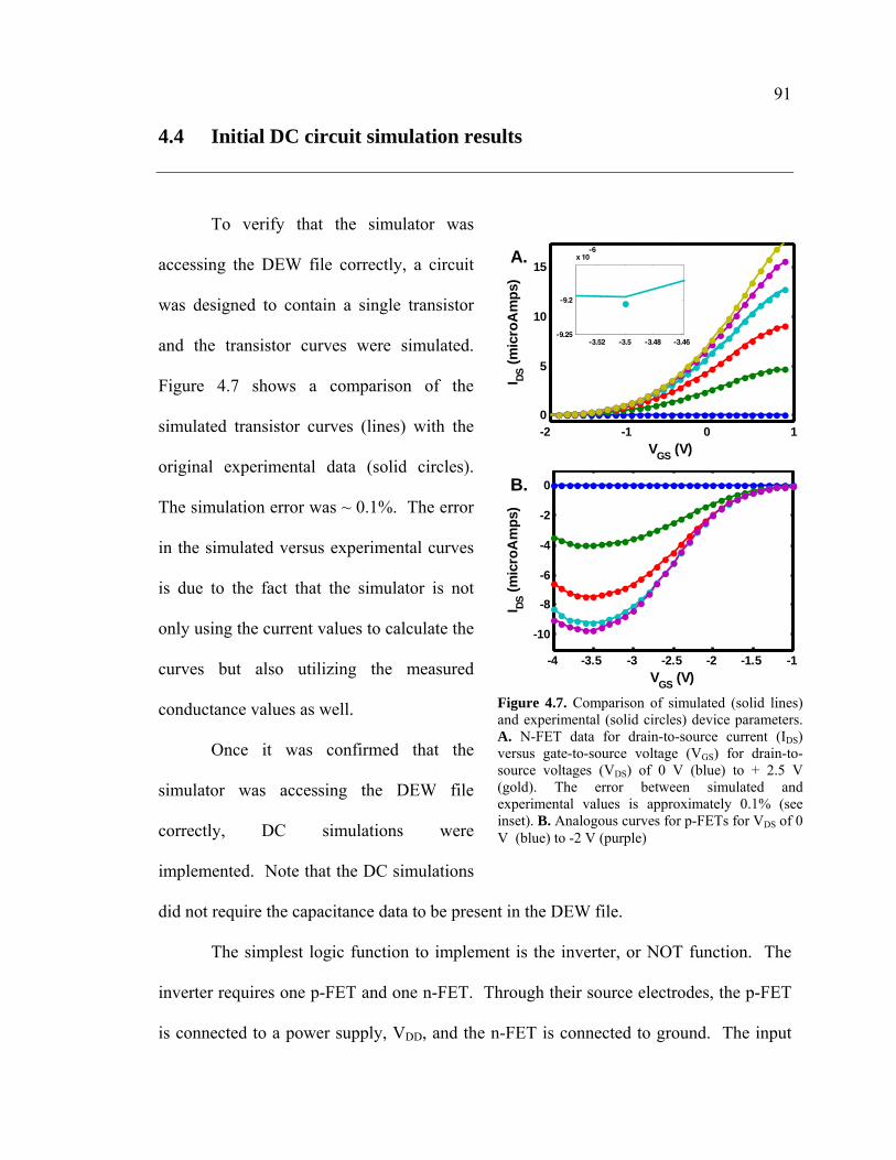
91 4.4 Initial DC circuit simulation results
To verify that the simulator was
accessing the DEW file correctly, a circuit
was designed to contain a single transistor
and the transistor curves were simulated.
Figure 4.7 shows a comparison of the
simulated transistor curves (lines) with the
original experimental data (solid circles).
The simulation error was ~ 0.1%. The error
in the simulated versus experimental curves
is due to the fact that the simulator is not
only using the current values to calculate the
curves but also utilizing the measured
conductance values as well.
Once it was confirmed that the
simulator was accessing the DEW file
correctly, DC simulations were
implemented. Note that the DC simulations
did not require the capacitance data to be present in the DEW file.
The simplest logic function to implement is the inverter, or NOT function. The
inverter requires one p-FET and one n-FET. Through their source electrodes, the p-FET
is connected to a power supply, VDD, and the n-FET is connected to ground. The input
-2 -1 0 10
5
10
15
VGS (V)
I DS (m
icro
Am
ps)
-4 -3.5 -3 -2.5 -2 -1.5 -1
-10
-8
-6
-4
-2
0
VGS (V)
I DS (m
icro
Am
ps)
A.
B.
-3.52 -3.5 -3.48 -3.46-9.25
-9.2
x 10-6
Figure 4.7. Comparison of simulated (solid lines) and experimental (solid circles) device parameters. A. N-FET data for drain-to-source current (IDS) versus gate-to-source voltage (VGS) for drain-to-source voltages (VDS) of 0 V (blue) to + 2.5 V (gold). The error between simulated and experimental values is approximately 0.1% (see inset). B. Analogous curves for p-FETs for VDS of 0 V (blue) to -2 V (purple)
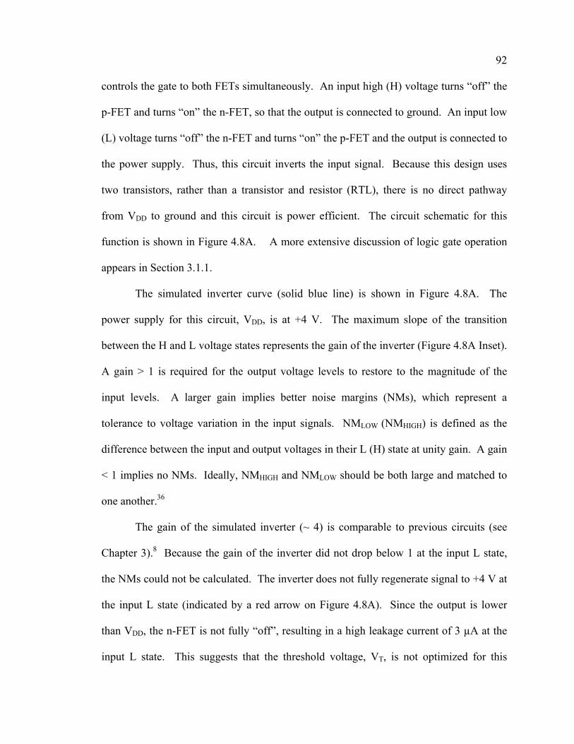
92 controls the gate to both FETs simultaneously. An input high (H) voltage turns “off” the
p-FET and turns “on” the n-FET, so that the output is connected to ground. An input low
(L) voltage turns “off” the n-FET and turns “on” the p-FET and the output is connected to
the power supply. Thus, this circuit inverts the input signal. Because this design uses
two transistors, rather than a transistor and resistor (RTL), there is no direct pathway
from VDD to ground and this circuit is power efficient. The circuit schematic for this
function is shown in Figure 4.8A. A more extensive discussion of logic gate operation
appears in Section 3.1.1.
The simulated inverter curve (solid blue line) is shown in Figure 4.8A. The
power supply for this circuit, VDD, is at +4 V. The maximum slope of the transition
between the H and L voltage states represents the gain of the inverter (Figure 4.8A Inset).
A gain > 1 is required for the output voltage levels to restore to the magnitude of the
input levels. A larger gain implies better noise margins (NMs), which represent a
tolerance to voltage variation in the input signals. NMLOW (NMHIGH) is defined as the
difference between the input and output voltages in their L (H) state at unity gain. A gain
< 1 implies no NMs. Ideally, NMHIGH and NMLOW should be both large and matched to
one another.36
The gain of the simulated inverter (~ 4) is comparable to previous circuits (see
Chapter 3).8 Because the gain of the inverter did not drop below 1 at the input L state,
the NMs could not be calculated. The inverter does not fully regenerate signal to +4 V at
the input L state (indicated by a red arrow on Figure 4.8A). Since the output is lower
than VDD, the n-FET is not fully “off”, resulting in a high leakage current of 3 µA at the
input L state. This suggests that the threshold voltage, VT, is not optimized for this
93 device and the device is always “on”, regardless of applied gate bias. Also, the center of
the inverter curve is shifted towards the input L state, indicating the n-FET has a larger
saturation current than the p-FET.36
The fabricated large-area FETs were also connected in the inverter configuration
(using off-chip connections) and measured. The experimental DC transfer characteristics
are shown in Figure 4.8A (dashed green line). This curve had many similar
characteristics to the predicted inverter curve. The measured inverter has a comparable
gain (~ 7.5) and NMs also could not be calculated. It also lacks signal restoration at the
input L state, and is not symmetric over VDD/2.
This mismatch in FET performance becomes more apparent as the circuits
become more complex. Figure 4.8B presents the simulated XOR circuit, which
comprises 6 p-FETs and 6 n-FETs. This circuit contains two inputs, which are
represented on the graph as the dashed blue line and the dotted green line. For the XOR
A.
0 1 2 3 40
1
2
3
4
Input (V)
Out
put (
V)
VDD
VIN VOUT
0 2 4-4.5
0
0 5 10 15 20
0
1
2
3
4
Time (microsec)
Volta
ge (V
)
B. A.
0 1 2 3 40
1
2
3
4
Input (V)
Out
put (
V)
VDD
VIN VOUT
0 2 4-4.5
0
0 5 10 15 20
0
1
2
3
4
Time (microsec)
Volta
ge (V
)
B.
Figure 4.8. DC simulation results of the inverter and XOR logic gates. A. Input versus output voltages of initial simulated (solid blue line) and fabricated (dashed green line) inverter. The red arrow indicates where the output voltage is not restoring to the power supply, VDD. Left Inset: Circuit schematic of CS inverter. Right Inset: Simulated inverter gain as a function of input voltage. B. Transient analysis of XOR gate with two inputs (dashed blue line and dotted green line). The output (solid red line) does not match the truth table for this function suggesting a mismatch in NW FET performance.
94 logic gate, when the two inputs are different (i.e., one is in the H state, the other in the L
state), the output should be in the H state. However, for the simulated NW circuit, this
does not occur and the function fails to go to its H state (VDD = +4 V). Integrated circuits
are comprised of several connected logic gates (for instance, a 2-bit half adder can be
generated by coupling a XOR gate with an AND gate) and thus with these devices as-
fabricated, more complex computations would fail.
4.5 Transient analysis circuit simulation results
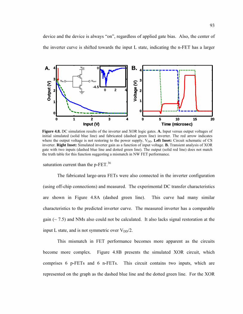
To verify that the capacitance elements in the DEW file were correct and being
accessed by the simulator correctly, the propagation delay, tpd, of the inverter circuit was
calculated and compared to the simulated results. This metric constitutes the time
difference between the mid point of the input swing and the mid point of the output
swing, and can be used to estimate the speed of complex circuits.37 Propagation delay
can be calculated from:
)(2 SATD
DDLpd I
VCt⋅⋅
= (4.8)
where CL is the load capacitance and ID(SAT) is the saturation current for the FET. To
measure the propagation delay, the inverter circuit was designed using a second inverter
as the load capacitance (Figure 4.9). Since the measured gate capacitance is ~ 0.35 pF for
one device, the total load capacitance is ~ 0.7 pF, ignoring any wiring capacitance. VDD
= +4 V for this circuit and the saturation currents for the n-FET and the p-FET are 9 µA
95 and 100 µA, respectively. This leads to a
calculated tdr = 160 ns and a tdf = 14 ns.
The total propagation delay, which is the
average of the rise and fall delays, is 87 ns.
The same inverter circuit with CL was also
examined in the simulation environment.
In Figure 4.9, the transition midpoints for
the input (dashed blue line) and the output
(solid green line) are denoted by red
arrows. The simulated propagation delay
values are tdr = 180 ns and a tdf = 20 ns, which equals a total propagation delay of 100 ns.
The good agreement between the simulated and calculated delay values demonstrates the
accuracy of the tabular model-based simulations for transient metrics.
4.6 Optimized DC circuit simulation results
To explore the effects on the inverter circuit by altering the NW FET
performance, two aspects of the simulation were modified. First, the number of NWs per
device were scaled to 10:1 (p-FET: n-FET), to match the saturation current levels.
Second, a battery element that offset the input voltage for the n-FET was incorporated
into the simulated circuit (see Figure 4.10A). The addition of the battery mimicked the
2 4 6 8 10-2
0
2
4
6
8
Time (microSeconds)
Volta
ge (V
)
VDD
VinVout
CL
VDD
VinVout
CL
2 4 6 8 10-2
0
2
4
6
8
Time (microSeconds)
Volta
ge (V
)
VDD
VinVout
CL
VDD
VinVout
CL
2 4 6 8 10-2
0
2
4
6
8
Time (microSeconds)
Volta
ge (V
)
VDD
VinVout
CL
VDD
VinVout
CL
Figure 4.9. Simulated transient plot of inverter. Input voltage is the dashed blue line. Output voltage is the solid green line. Red arrows denote the 50% point of the voltage transitions. Inset: Circuit schematic of inverter with load capacitance, CL
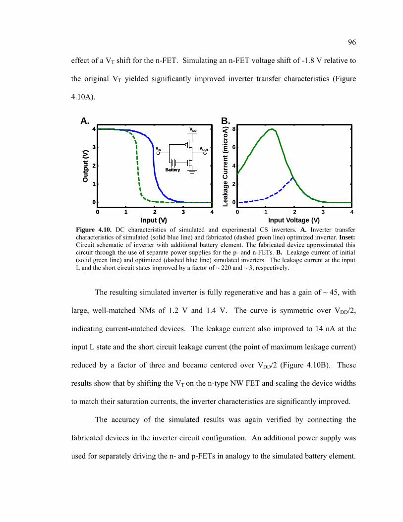
96 effect of a VT shift for the n-FET. Simulating an n-FET voltage shift of -1.8 V relative to
the original VT yielded significantly improved inverter transfer characteristics (Figure
4.10A).
The resulting simulated inverter is fully regenerative and has a gain of ~ 45, with
large, well-matched NMs of 1.2 V and 1.4 V. The curve is symmetric over VDD/2,
indicating current-matched devices. The leakage current also improved to 14 nA at the
input L state and the short circuit leakage current (the point of maximum leakage current)
reduced by a factor of three and became centered over VDD/2 (Figure 4.10B). These
results show that by shifting the VT on the n-type NW FET and scaling the device widths
to match their saturation currents, the inverter characteristics are significantly improved.
The accuracy of the simulated results was again verified by connecting the
fabricated devices in the inverter circuit configuration. An additional power supply was
used for separately driving the n- and p-FETs in analogy to the simulated battery element.
0 1 2 3 40
2
4
6
8
Input Voltage (V)Le
akag
e C
urre
nt (m
icro
A)
0 1 2 3 40
1
2
3
4
Input (V)
Out
put (
V)
VDD
VIN VOUT
Battery
VDD
VIN VOUT
Battery
0 1 2 3 40
1
2
3
4
Input (V)
Out
put (
V)
VDD
VIN VOUT
Battery
VDD
VIN VOUT
Battery
B.A.
Figure 4.10. DC characteristics of simulated and experimental CS inverters. A. Inverter transfer characteristics of simulated (solid blue line) and fabricated (dashed green line) optimized inverter. Inset: Circuit schematic of inverter with additional battery element. The fabricated device approximated this circuit through the use of separate power supplies for the p- and n-FETs. B. Leakage current of initial (solid green line) and optimized (dashed blue line) simulated inverters. The leakage current at the input L and the short circuit states improved by a factor of ~ 220 and ~ 3, respectively.
97 With an input voltage shift of -800 mV on the n-FET, the inverter exhibited full signal
restoration, NMs of 2.1 V (H) and 1 V (L), and a gain of ~ 30 (Figure 4.10A dashed
green curve). The voltage swing shifted to the left due to the mismatched saturation
current levels of the n- and p-FETs, which was corrected in the simulations. Otherwise,
the curves are in good agreement with each other.
4.7 MEDICI simulations
To facilitate the designing of the NW n-FET device with a shifted VT, MEDICI
simulations were utilized. MEDICI (Synopsys Inc.) is a two-dimensional semiconductor
device simulator that models the potentials and carrier concentrations in a device for any
given biases.
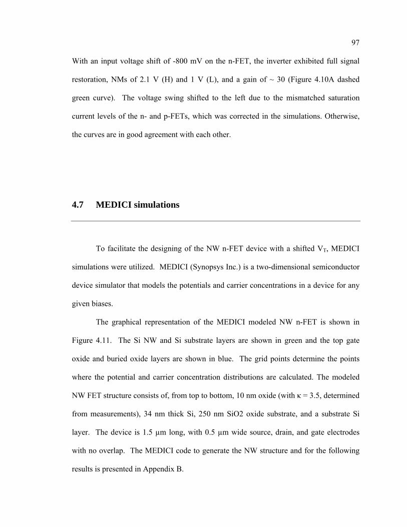
The graphical representation of the MEDICI modeled NW n-FET is shown in
Figure 4.11. The Si NW and Si substrate layers are shown in green and the top gate
oxide and buried oxide layers are shown in blue. The grid points determine the points
where the potential and carrier concentration distributions are calculated. The modeled
NW FET structure consists of, from top to bottom, 10 nm oxide (with κ = 3.5, determined
from measurements), 34 nm thick Si, 250 nm SiO2 oxide substrate, and a substrate Si
layer. The device is 1.5 µm long, with 0.5 µm wide source, drain, and gate electrodes
with no overlap. The MEDICI code to generate the NW structure and for the following
results is presented in Appendix B.
98
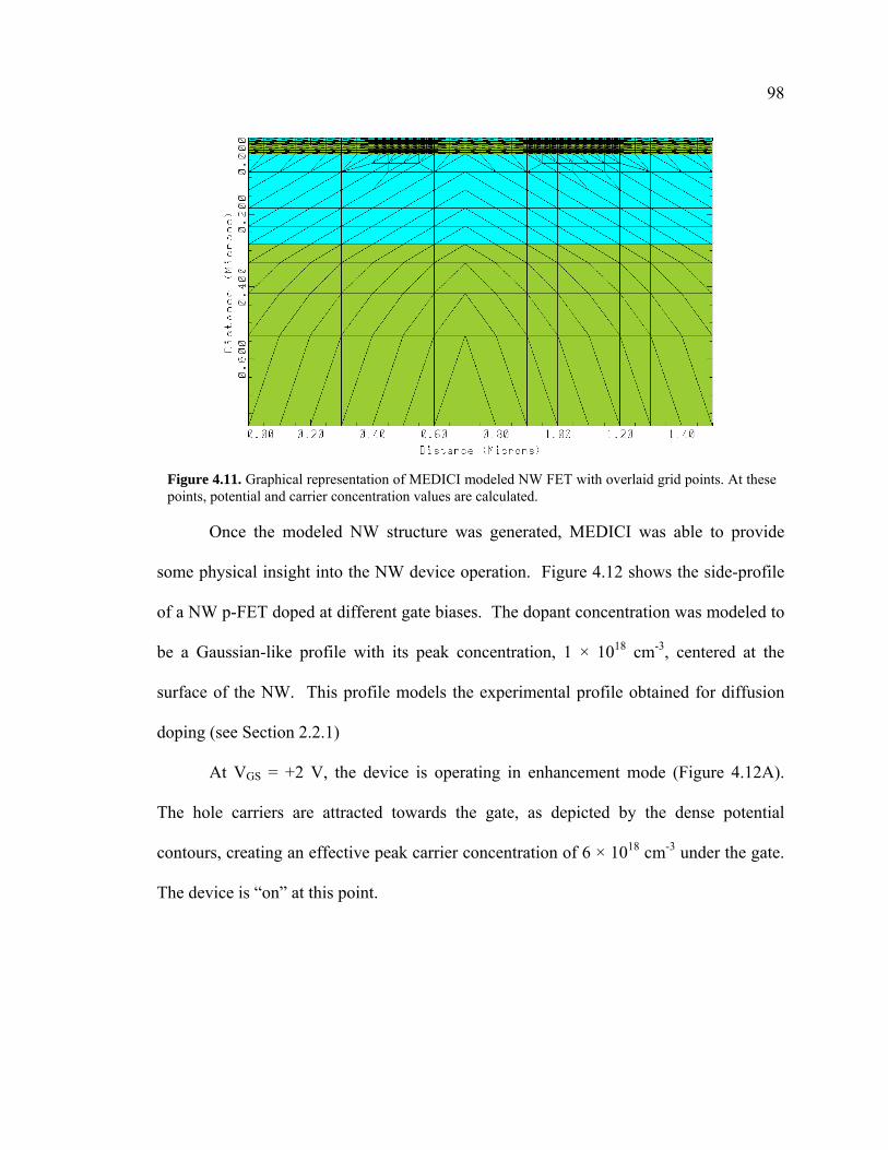
Once the modeled NW structure was generated, MEDICI was able to provide
some physical insight into the NW device operation. Figure 4.12 shows the side-profile
of a NW p-FET doped at different gate biases. The dopant concentration was modeled to
be a Gaussian-like profile with its peak concentration, 1 × 1018 cm-3, centered at the
surface of the NW. This profile models the experimental profile obtained for diffusion
doping (see Section 2.2.1)
At VGS = +2 V, the device is operating in enhancement mode (Figure 4.12A).
The hole carriers are attracted towards the gate, as depicted by the dense potential
contours, creating an effective peak carrier concentration of 6 × 1018 cm-3 under the gate.
The device is “on” at this point.
Figure 4.11. Graphical representation of MEDICI modeled NW FET with overlaid grid points. At these points, potential and carrier concentration values are calculated.
99
Next, at VGS = 0 V, a
depletion region forms under the
gate. This is due a mismatch of the
gate metal’s work function, ΦM, to
the electron affinity of the Si,
which leads to band bending at the
metal-oxide-Si interface.24 The
effective dopant concentration
directly underneath the gate drops
to 2 × 1017 cm-3.
Finally, at VGS = -2 V, the
negative bias repels the hole carriers from the channel and the depletion region grows
significantly larger. Consequently, the device conductivity drops and is “off” at this
point. The effective dopant concentration under the gate drops below 1 × 1015 cm-3
throughout the entire channel. The behavior of the modeled devices for different gate
biases is in agreement with experimental results and with the buried channel MOSFET
description used earlier to define VT and S.
Several NW parameters were varied, including the channel dopant profiles and
gate metals, using VT as feedback. The dopant profile of the device with the best VT
consisted of a uniform background n-type dopant concentration of 1014 cm-3 with
Gaussian-like NW dopant profiles having peak concentrations at the NW surface of 1016
cm-3 under the gate and 1019 cm-3 under the S/D contacts. Solutions for the IDS-VGS
curves were determined using models that took into account Shockley-Read-Hall
A.A.
B.B.
C.C.
Figure 4.12. NW device potential contours for different gate biases. A. Device operating in enhancement mode B. Zero gate bias on device. C. Device operating in depletion mode
100 recombination with carrier-dependent lifetimes, a concentration- and temperature-
dependent mobility, and an enhanced surface mobility at the semiconductor-insulator
interfaces due to scattering from phonons,
surface roughness, and charged
impurities.38 The Newton solution method
was used for both n- and p-type carriers.
For the simulated IDS-VGS curves, VDS was
fixed at 100 mV and VGS was measured in
50 mV steps. Both Ti and Pt gate electrode
metals were considered, as well as higher
channel doping (> 1018 cm-3).
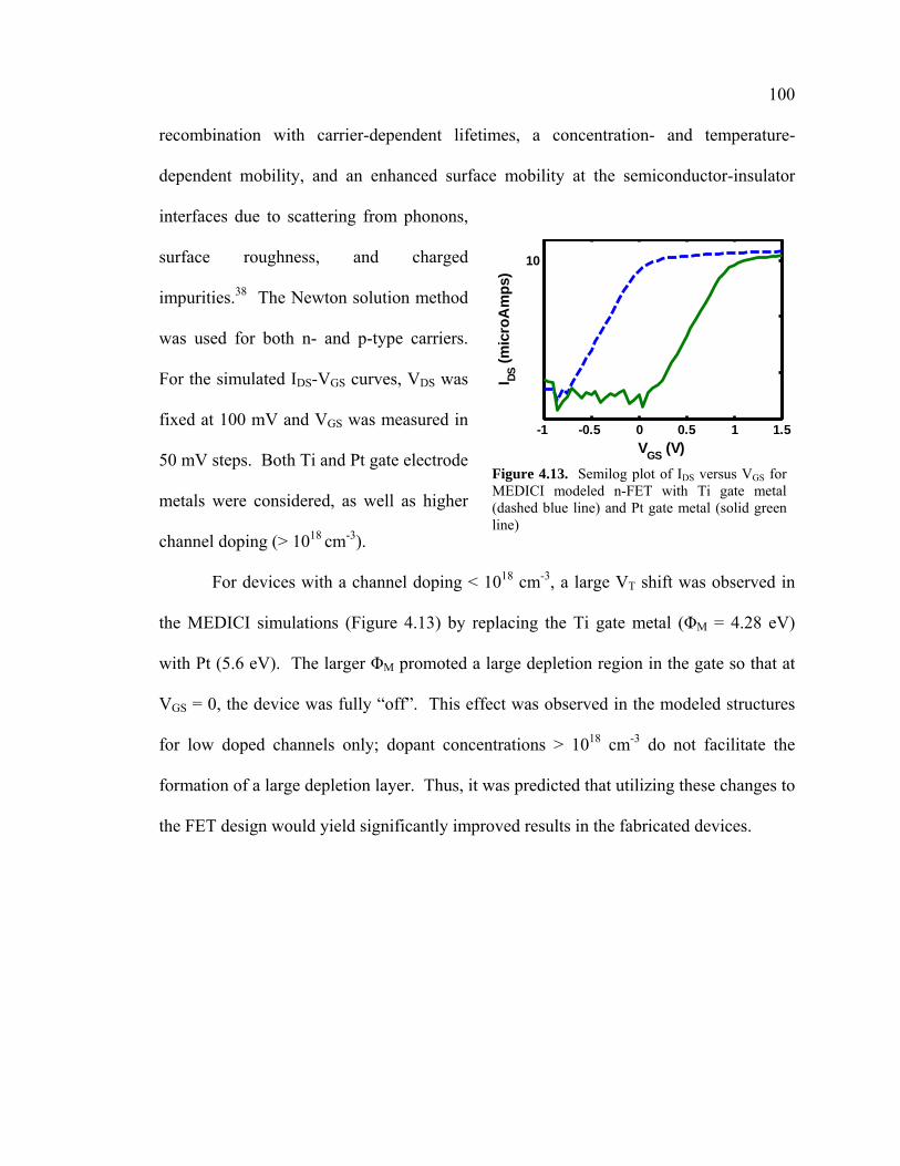
For devices with a channel doping < 1018 cm-3, a large VT shift was observed in
the MEDICI simulations (Figure 4.13) by replacing the Ti gate metal (ΦM = 4.28 eV)
with Pt (5.6 eV). The larger ΦM promoted a large depletion region in the gate so that at
VGS = 0, the device was fully “off”. This effect was observed in the modeled structures
for low doped channels only; dopant concentrations > 1018 cm-3 do not facilitate the
formation of a large depletion layer. Thus, it was predicted that utilizing these changes to
the FET design would yield significantly improved results in the fabricated devices.
-1 -0.5 0 0.5 1 1.5
10
VGS (V)
I DS (m
icro
Am
ps)
Figure 4.13. Semilog plot of IDS versus VGS for MEDICI modeled n-FET with Ti gate metal (dashed blue line) and Pt gate metal (solid green line)
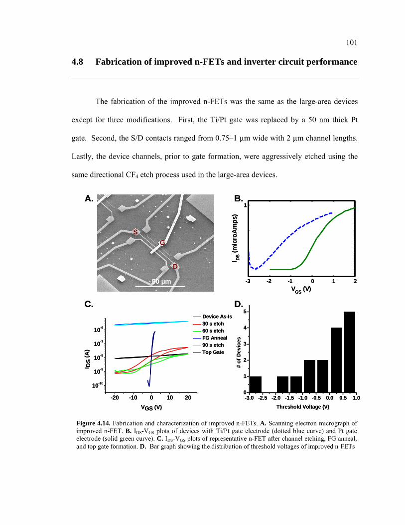
101 4.8 Fabrication of improved n-FETs and inverter circuit performance
The fabrication of the improved n-FETs was the same as the large-area devices
except for three modifications. First, the Ti/Pt gate was replaced by a 50 nm thick Pt
gate. Second, the S/D contacts ranged from 0.75–1 µm wide with 2 µm channel lengths.
Lastly, the device channels, prior to gate formation, were aggressively etched using the
same directional CF4 etch process used in the large-area devices.
50 µm
S
D
G
-3 -2 -1 0 1 2
1
VGS (V)
I DS (m
icro
Am
ps)
B.A.
-20 -10 0 10 20
10-10
10-9
10-8
10-7
10-6
Device As-Is 30 s etch 60 s etch FG Anneal 90 s etch Top Gate
I DS
(A)
VGS (V)
D.C.
-3.0 -2.5 -2.0 -1.5 -1.0 -0.5 0.0 0.5 1.00
1
2
3
4
5
# of
Dev
ices
Threshold Voltage (V)
50 µm
S
D
G
50 µm
S
D
G
-3 -2 -1 0 1 2
1
VGS (V)
I DS (m
icro
Am
ps)
B.A.
-20 -10 0 10 20
10-10
10-9
10-8
10-7
10-6
Device As-Is 30 s etch 60 s etch FG Anneal 90 s etch Top Gate
I DS
(A)
VGS (V)
D.C.
-3.0 -2.5 -2.0 -1.5 -1.0 -0.5 0.0 0.5 1.00
1
2
3
4
5
# of
Dev
ices
Threshold Voltage (V)
Figure 4.14. Fabrication and characterization of improved n-FETs. A. Scanning electron micrograph of improved n-FET. B. IDS-VGS plots of devices with Ti/Pt gate electrode (dotted blue curve) and Pt gate electrode (solid green curve). C. IDS-VGS plots of representative n-FET after channel etching, FG anneal, and top gate formation. D. Bar graph showing the distribution of threshold voltages of improved n-FETs

102 Figure 4.14A shows the scanning electron micrograph of the fabricated
transistors. Three transistors of varying widths were fabricated per top gate electrode.
The Pt gate is evident by its brightness in the image, due to the higher work function of
the metal. IDS – VGS measurements were taken of the Pt gate n-FETs and compared with
devices fabricated with Ti/Pt gates. The comparison is shown in Figure 4.14B. A large
VT shift was observed, in agreement with the MEDICI results (Figure 4.13).
The large observed VT shift was also due to more careful control over the channel
etching procedure. For the original n-FETs, back-gating measurements were first
performed after approximately three minutes of channel etching and then after one
minute cycles. For the improved n-FET devices, measurements were performed after
every 30 s of etching (see Figure 4.14C). Current hysteresis, caused by the interface
damage induced by the etching process, was observed after a few etch cycles and could
be reduced by a FG anneal. Care was taken so that the optimal etch time was not
exceeded.
It was observed during the channel etching that the FET devices did not have
identical performance characteristics. Figure 4.14D gives the distribution of threshold
voltages for the fabricated improved n-FET devices. The majority of devices have VT > 0
V. High-channel doping (due to variations introduced the doping and etching processes)
led to the negative VT, which can be shown by looking at the device on/off ratios. The
devices with VT > 0 V had an average on/off ratio of 2.4 × 10⁴, whereas the devices with
VT < 0 V had an average on/off ratio of 5.5 × 10². Both sets of devices have similar “on”
currents (in the low µA range) so the lowered on/off ratio is likely indicative of higher
channel doping which screens against the gate.
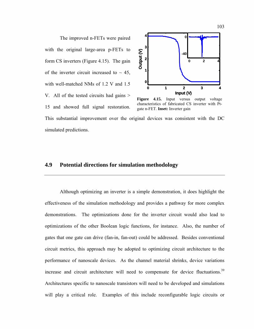
103 The improved n-FETs were paired
with the original large-area p-FETs to
form CS inverters (Figure 4.15). The gain
of the inverter circuit increased to ~ 45,
with well-matched NMs of 1.2 V and 1.5
V. All of the tested circuits had gains >
15 and showed full signal restoration.
This substantial improvement over the original devices was consistent with the DC
simulated predictions.
4.9 Potential directions for simulation methodology
Although optimizing an inverter is a simple demonstration, it does highlight the
effectiveness of the simulation methodology and provides a pathway for more complex
demonstrations. The optimizations done for the inverter circuit would also lead to
optimizations of the other Boolean logic functions, for instance. Also, the number of
gates that one gate can drive (fan-in, fan-out) could be addressed. Besides conventional
circuit metrics, this approach may be adopted to optimizing circuit architecture to the
performance of nanoscale devices. As the channel material shrinks, device variations
increase and circuit architecture will need to compensate for device fluctuations.39
Architectures specific to nanoscale transistors will need to be developed and simulations
will play a critical role. Examples of this include reconfigurable logic circuits or
0 1 2 3 40
1
2
3
4
Input (V)
Out
put (
V)
0 2 4
-40
0
0 1 2 3 40
1
2
3
4
Input (V)
Out
put (
V)
0 2 4
-40
0
Figure 4.15. Input versus output voltage characteristics of fabricated CS inverter with Pt-gate n-FET. Inset: Inverter gain
104 asynchronous logic design, where the high-performance FETs can be used efficiently and
the low-performance FETS can be used in non-critical areas or not used at all.
Another important area that will need to be addressed more in-depth is device and
circuit operating speed. Preliminary transient analyses were performed that highlighted
the accuracy of the table look-up model but no optimizations were done. Transient
analyses of circuits could be used as feedback for improving device speed, in an
analogous method for optimizing DC metrics. This would allow for the efficient
fabrication of circuits that require high frequency or high speed, such as a ring oscillator.
4.10 Conclusions
Si NW n-FETs and p-FETs were optimized using in silico circuit and device
simulations in feedback with device fabrication methods to produce complementary
symmetry inverters. Inverters with gains of 15–45, well-matched noise margins, and full
signal restoration were demonstrated. The presented method provides a highly efficient
means for optimizing nanowire logic circuits and is accurate for both DC and transient
analysis. By incorporating CAD simulation tools into the design process, nanocircuits
can be efficiently optimized and evaluated.
105 4.11 References
1. Chau, R.; Datta, S.; Doczy, M.; Doyle, B.; Jin, B.; Kavalieros, J.; Majumdar, A.; Metz, M.; Radosavljevic, M. Benchmarking Nanotechnology for High-Performance and Low-Power Logic Transistor Applications. IEEE Trans. Nanotech. 2005, 4, 153–158.
2. Brar, B.; Li, J. C.; Pierson, R. L.; Higgins, J. A. In InP HBTs- Present Status and Future Trends, IEEE Bipolar/BiCMOS Circuits and Technology Meeting, 2002, 155–161.
3. Datta, S. III-V field-effect transistors for low power digital logic applications. Microelectron. Engi. 2007, 84, 2133–2137.
4. Ma, B. Y.; Bergman, J.; Chen, P.; Hacker, J. B.; Sullivan, G.; Nagy, G.; Brar, B. InAs/AlSb HEMT and Its Application to Ultra-Low-Power Wideband High-Gain Low-Noise Amplifiers. IEEE Trans. Microwave Theory Tech. 2006, 54, 4448–4455.
5. Huang, Y.; Duan, X. F.; Cui, Y.; Lauhon, L. J.; Kim, K. H.; Lieber, C. M. Logic Gates and Computation from Assembled Nanowire Building Blocks. Science 2001, 294, 1313–1317.
6. Goldberger, J.; Hochbaum, A. I.; Fan, R.; Yang, P. D. Silicon Vertically Integrated Nanowire Field Effect Transistors. Nano Lett. 2006, 6, 973–977.
7. Wang, D.; Sheriff, B. A.; Heath, J. R. Silicon p-FETs from Ultrahigh Density Nanowire Arrays. Nano Lett. 2006, 6, 1096–1100.
8. Wang, D. W.; Sheriff, B. A.; Heath, J. R. Complementary Symmetry Silicon Nanowire Logic: Power-Efficient Inverters with Gain. Small 2006, 2, 1153–1158.
9. Deryche, V.; Martel, R.; Appenzeller, J.; Avouris, P. Carbon Nanotube Inter- and Intramolecular Logic Gates. Nano Lett. 2001, 1, 453–456.
10. Liu, X.; Lee, C.; Zhou, C.; Han, J. Carbon Nanotube Field-Effect Inverters. Appl. Phys. Lett. 2001, 79, 3329–3331.
11. Avouris, P.; Martel, R.; Derycke, V.; Appenzeller, J. Carbon Nanotube Transistors and Logic Circuits. Physica B 2002, 323, 6–12.
12. Javey, A.; Kim, H.; Brink, M.; Wang, Q.; Ural, A.; Guo, J.; Mcintyre, P.; McEuen, P.; Lundstrom, M.; Dai, H. High-k Dielectrics for Advanced Carbon-Nanotube Transistors and Logic Gates. Nat. Mater. 2002, 1, 241–246.
106 13. Javey, A.; Wang, Q.; Ural, A.; Li, Y. M.; Dai, H. J. Carbon Nanotube Transistor
Arrays for Multistage Complementary Logic and Ring Oscillators. Nano Lett. 2002, 2, 929–932.
14. Bachtold, A.; Hadley, P.; Nakanishi, T.; Dekker, C. Logic Circuits with Carbon Nanotube Transistors. Science 2001, 294, 1317–1320.
15. Appenzeller, J.; Lin, Y.-M.; Knoch, J.; Avouris, P. Band-to-Band Tunneling in Carbon Nanotube Field-Effect Transistors. Phys. Rev. Lett. 2004, 93, 196805–196809.
16. Hu, P. a.; Xiao, K.; Liu, Y.; Yu, G.; Wang, X.; Fu, L.; Cui, G.; Zhu, D. Multiwall nanotubes with intramolecular junctions (CNx/C): Preparation, rectification, logic gates, and application. Appl. Phys. Lett. 2004, 84, 4932–4934.
17. Friedman, R. S.; McAlpine, M. C.; Ricketts, D. S.; Ham, D.; Lieber, C. M. High-Speed Integrated Nanowire Circuits. Nature 2005, 434, 1085–1085.
18. Raychowdhury, A.; Keshavarzi, A.; Kurtin, J. N.; De, V.; Roy, K. Carbon Nanotube Field-Effect Transistors for High-Performance Digital Circuits: DC Analysis and Modeling Toward Optimum Transistor Structure. IEEE Trans. Electron Devices 2006, 53, 2711–2717.
19. Keshavarzi, A.; Raychowdhury, A.; Kurtin, J. N.; Roy, K.; De, V. Carbon Nanotube Field-Effect Transistors for High-Performance Digital Circuits-Transient Analysis, Parasitics, and Scalability. IEEE Trans. Electron Devices 2006, 53, 2718–2726.
20. Bindal, A.; Hamedi-Hagh, S. The Impact of Silicon Nano-Wire Technology on the Design of Single-Work-Function CMOS Transistors and Circuits. Nanotech 2006, 17, 4340–4351.
21. Sheriff, B. A.; Wang, D.; Kurtin, J. N.; Heath, J. R. Complementary Symmetry Nanowire Logic Circuits: Experimental Demonstrations and In Silico Optimizations. ACS Nano 2008 (revisions submitted 3/14/08).
22. Melosh, N. A.; Boukai, A.; Diana, F.; Gerardot, B.; Badolato, A.; Petroff, P. M.; Heath, J. R. Ultrahigh-Density Nanowire Lattices and Circuits. Science 2003, 112–115.
23. Ilani, S.; Donev, L. A. K.; Kindermann, M.; McEuen, P. L. Measurement of the Quantum Capacitance of Interacting Electrons in Carbon Nanotubes. Nat. Phys. 2006, 2, 687–691.
24. Pierret, R. F. Field Effect Devices. (Second ed.) Addison-Wesley Publishing Company: Reading, Massachusetts, 1990 (vol. 4, p. 203).
107 25. Oka, H.; Nishiuchi, K.; Nakamura, T.; Ishikawa, H. Computer Analysis of a
Short-Channel BC MOSFET. IEEE J. Solid-State Circuits 1980, SC-15, (4), 579–585.
26. Wordeman, M. R.; Dennard, R. H. Threshold Voltage Characteristics of Depletion-Mode MOSFET's. IEEE Trans. Electron Devices 1981, ED-28, 1025–1030.
27. Sze, S. M. Physics of Semiconductor Devices. (Second ed.) John Wiley & Sons, Inc.: New York, NY, 1981.
28. Hendrickson, T. E. A Simplified Model for Subpinchoff Conduction in Depletion-Mode IGFET's. IEEE Trans. Electron Devices 1978, ED-25, 435–441.
29. Koo, S. M.; Li, Q.; Monica, D. E.; Richter, C. A.; Vogel, E. M. Enhanced Channel Modulation in Dual-Gated Silicon Nanowire Transistors. Nano Lett. 2005, 5, 2519–2523.
30. Shamarao, P.; Ozturk, M. C. A Study on Channel Design for 0.1 um Buried p-Channel MOSFET's. IEEE Trans. Electron Devices 1996, 43, 1942–1949.
31. Shima, T.; Sugawara, T.; Moriyama, S.; Yamada, H. Three-Dimensional Table Look-Up MOSFET Model for Precise Circuit Simulation. IEEE J. Solid-State Circuits 1982, SC-17, 449–454.
32. Meijer, P. B. L. Fast and Smooth Highly Nonlinear Multidimensional Table Models for Device Modeling. IEEE Trans. Circuits Syst. 1990, 37, 335–346.
33. Mohan, S.; Sun, J. P.; Mazumder, P.; Haddad, G. I. Device and Circuit Simulations of Quantum Electronic Devices. IEEE Trans. Comput. Aided Des. Integrat. Circuits Syst. 1995, 14, 653–662.
34. Wei, C.-J.; Tkachenko, Y. A.; Bartle, D. Table-Based Dynamics FET Model Assembled From Small-Signal Models. IEEE Trans. Microwave Theory Tech. 1999, 47, 700–705.
35. Agilent 4284A/4285A Precision LCR Meter Family Technical Overview. Agilent Technologies, Inc., 2008.
36. Sedra, A. S.; Smith, K. C. Microelectronic Circuits. (Fourth ed.) Oxford University Press: New York, 1997.
37. Gajski, D. D. Principles of Digitial Design. Prentice-Hall, Inc.: Upper Saddle River, NJ, 1997.
38. MEDICI:Two-Dimensional Device Simulation Program: User Manual (Version 2002.4). Synopsys, Inc., 2003.

108 39. Asenov, A. Simulation of Statistical Variability in Nano MOSFETs. VLSI Tech.
Dig. Tech. Pap. 2007, 86–87.
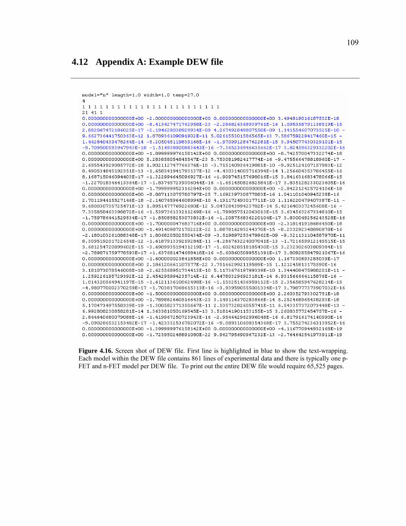
109 4.12 Appendix A: Example DEW file
Figure 4.16. Screen shot of DEW file. First line is highlighted in blue to show the text-wrapping. Each model within the DEW file contains 861 lines of experimental data and there is typically one p-FET and n-FET model per DEW file. To print out the entire DEW file would require 65,525 pages.

110 4.13 Appendix B: MEDICI code
P-FET structure MEDICI Code: TITLE P-type Si NW FET on SiO2 COMMENT Specify a rectangular mesh MESH SMOOTH=1 COMMENT Specify mesh dimensions X.MESH WIDTH=1.0 H1=0.1 Y.MESH N=1 L=-0.005 Y.MESH N=2 L=0.0 Y.MESH DEPTH=.034 H1=0.01 H2=0.01 Y.MESH DEPTH=.25 SPACING=0.05 Y.MESH DEPTH=.5 SPACING=0.25 COMMENT Regions REGION NAME=Gate_Ox Y.MAX=0 HFO2 REGION NAME=NW Y.MIN=0.0 Y.MAX=0.034 SILICON REGION NAME=Box Y.MIN=0.034 Y.MAX=.284 OXIDE REGION NAME=Bulk Y.MIN=0.284 SILICON COMMENT Electrodes ELECTR NAME=Gate X.MIN=.3 X.MAX=.7 + TOP ELECTR NAME=Source X.MAX=0.4 Y.MIN=-0.001 + Y.MAX=0.0 ELECTR NAME=Drain X.MIN=.6 Y.MIN=-0.001 + Y.MAX=0.0 ELECTR NAME=Substrate BOTTOM COMMENT Specify impurity profiles and fixed charges PROFILE P-TYPE N.PEAK=1e15 UNIFORM + OUT.FILE=pfetdop1 COMMENT PROFILE P-TYPE N.PEAK=1e18 Y.MIN=0 COMMENT DEPTH=0.01 COMMENT + Y.JUNCTI=0.034 COMMENT Plot initial Grid PLOT.2D GRID FILL SCALE TITLE="Simulation Mesh" COMMENT Regrid on doping REGRID DOPING LOG IGNORE=Box RATIO=2 SMOOTH=1 + IN.FILE=pfetdop1 PLOT.2D GRID TITLE="DOPING" FILL SCALE

111 COMMENT Pt's workfunction is 5.6 CONTACT NAME=(Gate,Source,Drain) WORKFUNC=4.33 COMMENT MATERIAL REGION=Gate_Ox PERMITTI=9 MODELS CONMOB SRFMOB2 FLDMOB COMMENT Zero carriers SYMB CARRIERS=0 METHOD ICCG DAMPED SOLVE REGRID POTEN RATIO=0.1 SMOOTH=1 IGNORE=Box + COS.ANG=0.95 + IN.FILE=pfetdop1 + OUT.FILE=pfetpot1 PLOT.2D GRID TITLE="POTENTIAL" FILL SCALE PLOT.1D DOPING X.START=1.5 X.END=1.5 Y.START=0 + Y.END=1 Y.LOG TOP=1E20 BOT=1E14 POINTS + COLOR=2 PLOT.2D BOUND FILL MODELS CONSRH ARORA SRFMOB2 SYMB GUMM CARRIER=0 METHOD ICCG DAMPED SYMB NEWTON CARRIER=2 SOLVE OUT.FILE=pfetsolve
112 N-FET structure MEDICI code: TITLE N-type Si NW FET on SiO2 COMMENT Specify a rectangular mesh MESH SMOOTH=1 COMMENT Specify mesh dimensions X.MESH WIDTH=1.5 H1=0.1 Y.MESH N=1 L=-0.01 Y.MESH N=2 L=0.0 Y.MESH DEPTH=.034 H1=0.01 H2=0.01 Y.MESH DEPTH=.25 SPACING=0.05 Y.MESH DEPTH=.5 SPACING=0.25 COMMENT Regions REGION NAME=Gate_Ox Y.MIN=-0.01 Y.MAX=0 OXIDE REGION NAME=NW Y.MIN=0.0 Y.MAX=0.034 SILICON REGION NAME=Box Y.MIN=0.034 Y.MAX=.284 OXIDE REGION NAME=Bulk Y.MIN=0.284 SILICON COMMENT Electrodes ELECTR NAME=Gate X.MIN=0.5 X.MAX=1 + TOP ELECTR NAME=Source X.MAX=0.5 Y.MIN=-0.005 + Y.MAX=0.0 ELECTR NAME=Drain X.MIN=1 Y.MIN=-0.005 + Y.MAX=0.0 ELECTR NAME=Substrate BOTTOM COMMENT Specify impurity profiles and fixed charges PROFILE N-TYPE N.PEAK=1E14 UNIFORM + OUT.FILE=nfetdop1 PROFILE N-TYPE N.PEAK=1E16 Y.MIN=0 DEPTH=0.005 + Y.JUNCTI=0.034 PROFILE N-TYPE N.PEAK=1E19 Y.JUNC=0.034 + X.MIN=0 WIDTH=0.5 PROFILE N-TYPE N.PEAK=1E19 Y.JUNC=0.034 + X.MIN=1 WIDTH=0.5 COMMENT Plot initial Grid PLOT.2D GRID FILL SCALE TITLE="Simulation Mesh" COMMENT Regrid on doping REGRID DOPING LOG IGNORE=Box RATIO=2 SMOOTH=1 + IN.FILE=nfetdop1 PLOT.2D GRID TITLE="DOPING" FILL SCALE COMMENT Ti's workfunction is 4.33; Al = 4.1

113 CONTACT NAME=Gate WORKFUNC=4.33 COMMENT MATERIAL REGION=Gate_Ox PERMITTI=3.5 MODELS SRFMOB2 ARORA CONSRH COMMENT Zero carriers SYMB CARRIERS=0 METHOD ICCG DAMPED SOLVE REGRID POTEN RATIO=0.1 SMOOTH=1 IGNORE=Box + COS.ANG=0.95 + IN.FILE=nfetdop1 + OUT.FILE=nfetpot1 PLOT.2D GRID TITLE="POTENTIAL" SCALE PLOT.1D DOPING X.START=0.75 X.END=0.75 Y.START=0 + Y.END=1 Y.LOG TOP=1E20 BOT=1E14 POINTS + COLOR=2 PLOT.2D BOUND FILL PLOT.1D DOPING X.START=0.25 X.END=0.25 Y.START=0 + Y.END=1 Y.LOG TOP=1E20 BOT=1E14 POINTS + COLOR=2 PLOT.2D BOUND FILL PLOT.1D X.START=0.75 X.END=0.75 Y.START=-0.005 Y.END=0.03 + COND NEG TITLE="Band Structure" TOP=4.5 BOTT=-4.5 PLOT.1D X.ST=0.75 X.END=0.75 Y.ST=-0.005 Y.END=0.03 + VAL UNCH NEG PLOT.1D X.START=0.75 X.END=0.75 Y.ST=-0.005 Y.END=0.03 + QFN UNCH NEG COL=2 PLOT.2D BOUND TITLE="Impurity Contours" FILL SCALE CONTOUR DOPING LOG MIN=14 MAX=19 DEL=0.5 COLOR=1 MODELS CONSRH ARORA SRFMOB2 SYMB GUMM CARRIER=0 METHOD ICCG DAMPED SOLVE SYMB NEWTON CARRIER=1 ELECTRON SOLVE SYMB NEWTON CARRIER=2 SOLVE OUT.FILE=nfetsolve SAVE MESH OUT.FILE=nfetAmesh W.MODELS

114 MEDICI code for generating potential contours TITLE pFET gate characteristics COMMENT Read in simulation mesh MESH IN.FILE=nfetpot1 LOAD IN.FILE=nfetsolve COMMENT initial solution COMMENT MODELS CONSRH ARORA SRFMOB2 COMMENT SYMB GUMM CARR=0 COMMENT SOLVE SYMB NEWTON CARRIERS=2 COMMENT Setup LOG file for solution LOG OUT.FILE=nfet_test1 COMMENT Solve for Vds=0.1 SOLVE V(Drain)=0.1 SOLVE V(Gate)=0 COMMENT Look at potential contours PLOT.2D BOUND JUNC DEPL FILL SCALE + TITLE="Potential Contours" Y.MAX=0.4 FILL REGION=NW COLOR=5 CONTOUR POTENTIA COMMENT look at carrier profile PLOT.1D HOLE X.START=.8 X.END=.8 Y.START=0 + Y.END=.03 POINTS + TITLE="Hole concentration under gate" PLOT.1D ELECTRON X.START=.8 X.END=.8 Y.START=0 + Y.END=.03 POINTS + TITLE="Electron concentration under gate" PLOT.2D FILL BOUND Y.MAX=0.2 + TITLE="Current flow" FILL REGION=NW COLOR=5 ^NP.COL CONTOUR FLOW
115 MEDICI code for generating IDS – VGS curves TITLE nFET gate characteristics COMMENT Read in simulation mesh MESH IN.FILE=nfetAmesh LOAD IN.FILE=nfetsolve SYMB NEWTON CARRIERS=2 COMMENT Setup LOG file for solution LOG OUT.FILE=nfet_gate2 COMMENT Solve for Vds=-0.1 and ramp gate SOLVE V(Drain)=0.1 SOLVE V(Gate)=-1 ELEC=Gate VSTEP=0.05 NSTEPS=50 COMMENT Plot Ids vs. Vgs PLOT.1D Y.AXIS=I(Drain) X.AXIS=V(gate) POINTS LOG COLOR=2 + TITLE="Ids vs. Vgs" LABEL LABEL="Vds is +100 mV" PLOT.1D X.START=0.75 X.END=0.75 Y.START=-0.005 Y.END=0.03 + COND NEG TITLE="Band Structure" TOP=4.5 BOTT=-4.5 PLOT.1D X.ST=0.75 X.END=0.75 Y.ST=-.005 Y.END=0.03 + VAL UNCH NEG PLOT.1D X.START=0.75 X.END=0.75 Y.ST=-.005 Y.END=0.03 + QFN UNCH NEG COL=2 EXTRACT MOS.PARA IN.FILE=nfet_gate2


![Synthesis of ZnO Nanowire Heterostructures by …ticle-assisted pulsed-laser deposition (NAPLD) [2,3]. Es-pecially, ZnO nanowire has attracted a great attention for building blocks](https://static.fdocument.pub/doc/165x107/5f478de1cf4db86df541cd98/synthesis-of-zno-nanowire-heterostructures-by-ticle-assisted-pulsed-laser-deposition.jpg)