
Big Ticket Items for DMT - IEEE 802 · Big Ticket Items for DMT . 2 - Hisaya Sakamoto, Fujitsu...
21
Sacha Corbeil, Ying Jiang, David Lewis, Brandon Collings IEEE 802.3bs Task Force March 10 th , 2015 Big Ticket Items for DMT
Transcript of Big Ticket Items for DMT - IEEE 802 · Big Ticket Items for DMT . 2 - Hisaya Sakamoto, Fujitsu...

Sacha Corbeil, Ying Jiang, David Lewis, Brandon Collings
IEEE 802.3bs Task Force March 10th, 2015
Big Ticket Items for DMT
2
- Hisaya Sakamoto, Fujitsu Optical Components - Hideki Isono, Fujitsu Optical Components - Tomoo Takahara, Fujitsu Ltd. - Toshiki Tanaka, Fujitsu Ltd. - Martin Bouda, Fujitsu US - Moonsoo Park, OE-Solution - Bongsin Kwark, OE-Solution - Ian Dedic, Socionext - Markus Weber, Socionext - Richard Castell, Socionext - Michael Kaushke, Socionext - Brian Teipen, Adva - Sven Krueger, H&S Cube Optics - Paul Brooks, JDSU T&M
Supporters

3
Big Ticket item overview/checklist Introduction and Purpose Proposed modifications to 10km DMT proposal Chromatic Dispersion Tolerance Cost and Power Comparison Summary Next Steps
Outline

4
Proposals • takahara_3bs_01_1114 (DMT)
Actions • Evaluate Coupling between
electrical and optical interfaces • RX Technical feasibility
• Dispersion penalty worst case
• TDP MPI
• RX sensitivity
• Optical loss budget model
• Interoperability
Big Ticket Item Overview and Checklist
update by May interim
this presentation (simulations) by May interim (measurements) tanaka_01_0215_smf & here (simulations) more measurements by May interim this presentation (simulations) tanaka_3bs_01a_0115 (measurements) this presentation (simulations) by May interim (measurements) update at May interim
update at May interim
• corbeil_3bs_01_0115 (DMT)
5
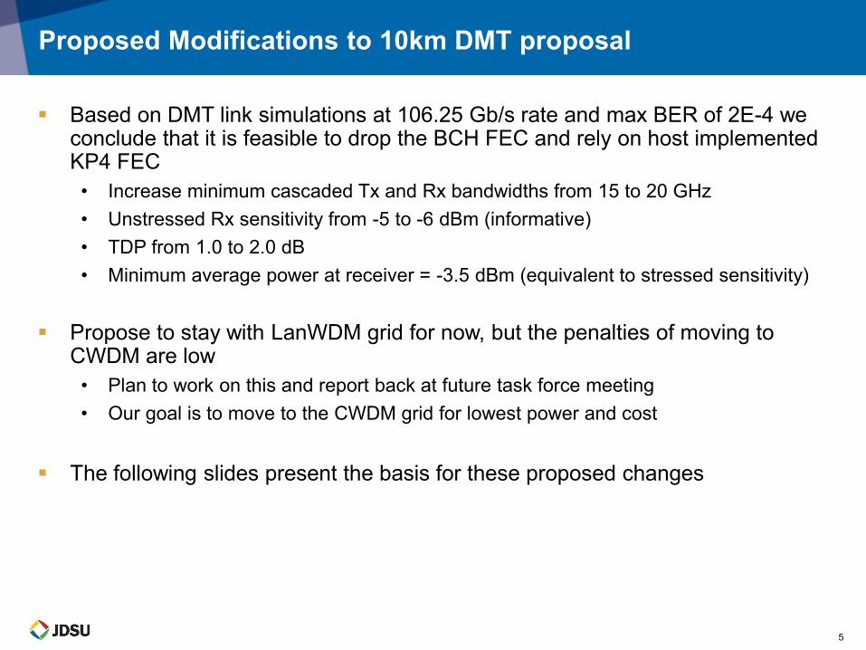
Based on DMT link simulations at 106.25 Gb/s rate and max BER of 2E-4 we conclude that it is feasible to drop the BCH FEC and rely on host implemented KP4 FEC
• Increase minimum cascaded Tx and Rx bandwidths from 15 to 20 GHz • Unstressed Rx sensitivity from -5 to -6 dBm (informative) • TDP from 1.0 to 2.0 dB • Minimum average power at receiver = -3.5 dBm (equivalent to stressed sensitivity)
Propose to stay with LanWDM grid for now, but the penalties of moving to
CWDM are low • Plan to work on this and report back at future task force meeting • Our goal is to move to the CWDM grid for lowest power and cost
The following slides present the basis for these proposed changes
Proposed Modifications to 10km DMT proposal
6
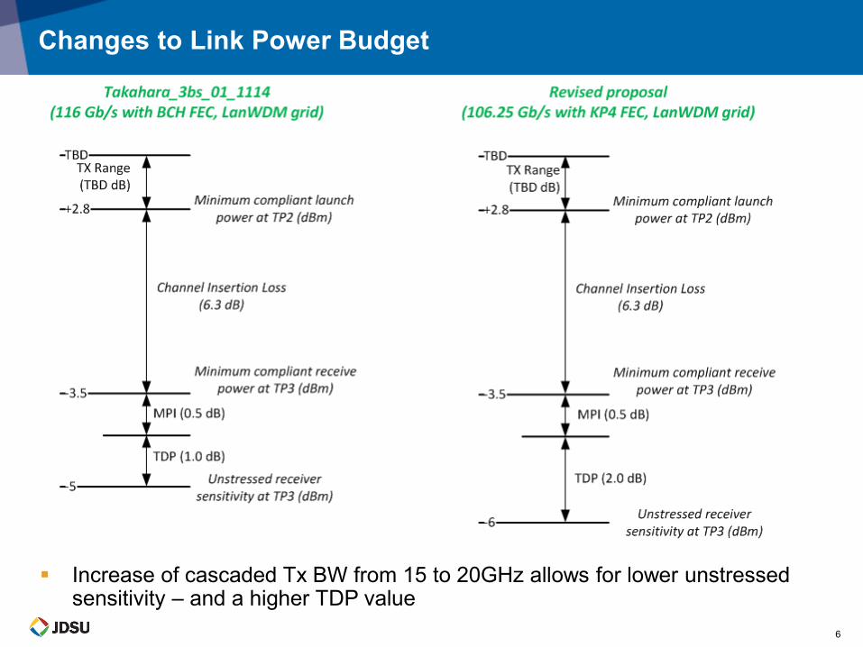
Increase of cascaded Tx BW from 15 to 20GHz allows for lower unstressed sensitivity – and a higher TDP value
Changes to Link Power Budget

7
Illustration of Sensitivity and TDP derivation
Reference RX
Minimum compliant RX
Reference TX
Minimum compliant TX
TDP ~ 2.0 dB

8
Using same realistic component parameters as for Nov’14 proposal, we demonstrate feasibility over the 10 km reach objective.
• OMA corresponds to optimal for performance at sensitivity. Approximately 10 dB at 2 GHz.
RIN: 1310 DFB • Integrated (average) -145 dB/Hz, • Peak ~ -138 dB/Hz near 7 GHz
Low IRN PIN-TIA • 12-15 pA/√Hz at High Gain
DMT Specifics: • Clipping Ratio of 3.16 (peak/RMS) • Cyclic-Prefix of 8 • Sample-Rate of 64 GS/s • 256 sub-carriers
KP4 for DMT – Feasibility Study
-7 -6 -5 -4 -3 -2 -1 0 1 2 3 410
-7
10-6
10-5
10-4
10-3
10-2
Rx Average Input Power [dBm]
BE
R
Summary for IEEE 802.3bs 10km DMT Link Budget
Target PIN-TIA, 20GHz @ ER=10.2
9K BCH FEC Threshold
KP4 FEC Threshold
Unstressed Sensitivity
Stressed Sensitivity
9
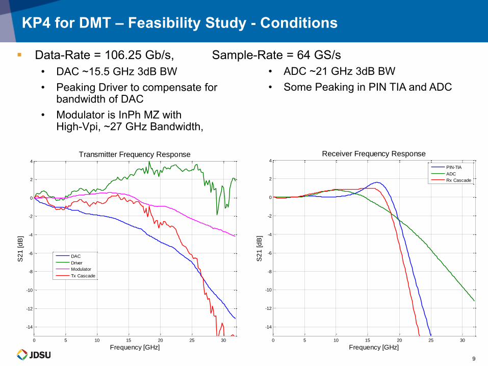
Data-Rate = 106.25 Gb/s, Sample-Rate = 64 GS/s • DAC ~15.5 GHz 3dB BW • Peaking Driver to compensate for
bandwidth of DAC • Modulator is InPh MZ with
High-Vpi, ~27 GHz Bandwidth,
KP4 for DMT – Feasibility Study - Conditions
0 5 10 15 20 25 30
-14
-12
-10
-8
-6
-4
-2
0
2
4
Frequency [GHz]
S2
1 [d
B]
Transmitter Frequency Response
DAC
Driver
Modulator
Tx Cascade
0 5 10 15 20 25 30
-14
-12
-10
-8
-6
-4
-2
0
2
4
Frequency [GHz]
S2
1 [d
B]
Receiver Frequency Response
PIN-TIA
ADC
Rx Cascade
• ADC ~21 GHz 3dB BW • Some Peaking in PIN TIA and ADC

10
KP4 Feasibility Study – Simulated BER contours at 116 Gb/s
Initial DMT research led us to requiring a high coding gain FEC, pushing the line-rate to 116 Gb/s due to overhead required to maintain low latency
We projected cascaded Tx & Rx Bandwidth each of ~15 GHz, placing us near the red X.
5.0 x 10 -52.0 x 10 -4
2.0 x 10 -4
8.0
x 1
0 -4
8.0 x 10 -4
8.0 x 10⁻⁴
3.3
x 1
0- 3
3.3
x 1
0 -3
3.3 x 10 -3
3.3 x 10⁻³
1.0 x 10 -2
Cascaded Tx Bandwidth [GHz]
Ca
sca
de
d R
x B
an
dw
idth
[G
Hz]
116 Gb/s DMT at 64 GS/s: Contours of Fixed BER at Rx Pwr = -5dBm
1.0x10⁻⁵
3.2x10⁻³
1.0x10⁻²
1.0x10⁻²
5.0x10-514 16 18 20 22 24 26
14
16
18
20
22
24
-4
-3.5
-3
-2.5
-2
X
Contours shown on this plot use ideal 4th order Bessel responses to mimic DAC, Driver, Modulator, ADC and PIN-TIA.
All three Tx components are kept equal in bandwidth in order to give desired cascaded bandwidth
Ditto for both Rx components.
Noise sources (RIN and IRN) same as in previous slides.

11
KP4 Feasibility Study– Simulated BER contours at 106.25 Gb/s
Lower line-rate of KP4 (106.25 Gb/s) helps in achieving better performance with same components.
Component availability in 2018 will yield higher bandwidth, placing us closer to the Green X.
1.0 x 10 -5
1.0 x 10 -5
5.0
x 1
0 -5
5.0 x 10 -5
5.0 x 10 -5
2.0
x 1
0 -4
2.0 x 10 -4
2.0 x 10 -4
8.0
x 1
0 -4
8.0 x 10 -4
8.0 x 10 -4
8.0 x 10⁻⁴
3.3
x 1
0 -3
Cascaded Tx Bandwidth [GHz]
Ca
sca
de
d R
x B
an
dw
idth
[G
Hz]
106.25 Gb/s DMT at 64 GS/s: Contours of Fixed BER at Rx Pwr = -5dBm
3.2x10⁻³
1.0x10-514 16 18 20 22 24 26
14
16
18
20
22
24
-5
-4.5
-4
-3.5
-3
-2.5
X
Data points (colored circles shows noise model simulations based on more realistic data, still using the Tx cascade 3dB BW as a figure of merit.
BER information is in color-coding: good match with generic component contour predictions.
12
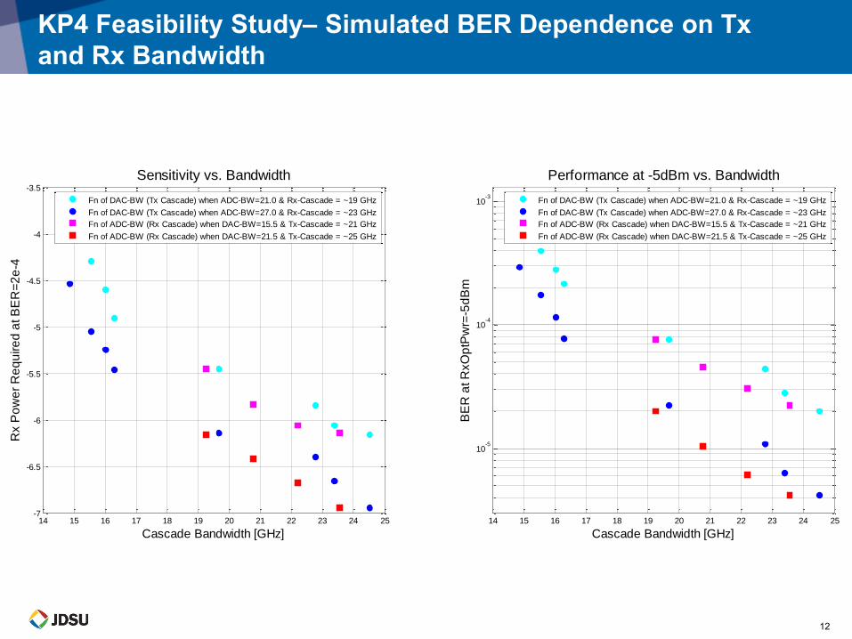
KP4 Feasibility Study– Simulated BER Dependence on Tx and Rx Bandwidth
14 15 16 17 18 19 20 21 22 23 24 25-7
-6.5
-6
-5.5
-5
-4.5
-4
-3.5
Cascade Bandwidth [GHz]
Rx P
ow
er
Re
qu
ire
d a
t B
ER
=2
e-4
Sensitivity vs. Bandwidth
Fn of DAC-BW (Tx Cascade) when ADC-BW=21.0 & Rx-Cascade = ~19 GHz
Fn of DAC-BW (Tx Cascade) when ADC-BW=27.0 & Rx-Cascade = ~23 GHz
Fn of ADC-BW (Rx Cascade) when DAC-BW=15.5 & Tx-Cascade = ~21 GHz
Fn of ADC-BW (Rx Cascade) when DAC-BW=21.5 & Tx-Cascade = ~25 GHz
14 15 16 17 18 19 20 21 22 23 24 25
10-5
10-4
10-3
Cascade Bandwidth [GHz]
BE
R a
t R
xO
ptP
wr=
-5d
Bm
Performance at -5dBm vs. Bandwidth
Fn of DAC-BW (Tx Cascade) when ADC-BW=21.0 & Rx-Cascade = ~19 GHz
Fn of DAC-BW (Tx Cascade) when ADC-BW=27.0 & Rx-Cascade = ~23 GHz
Fn of ADC-BW (Rx Cascade) when DAC-BW=15.5 & Tx-Cascade = ~21 GHz
Fn of ADC-BW (Rx Cascade) when DAC-BW=21.5 & Tx-Cascade = ~25 GHz
13
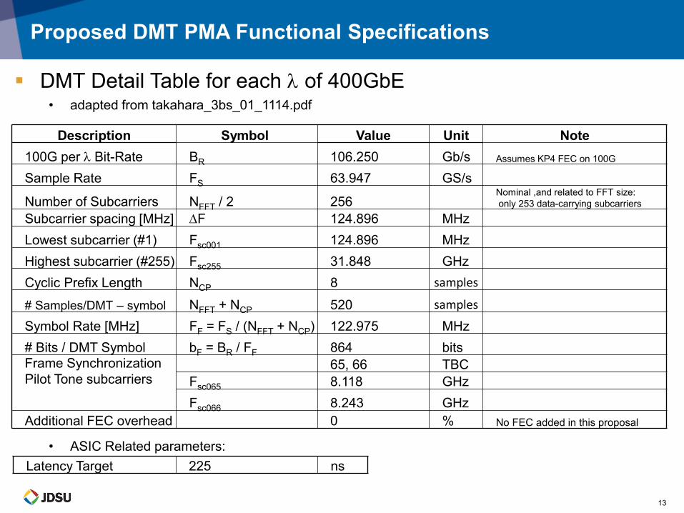
DMT Detail Table for each l of 400GbE • adapted from takahara_3bs_01_1114.pdf
• ASIC Related parameters:
Proposed DMT PMA Functional Specifications
Description Symbol Value Unit Note 100G per l Bit-Rate BR 106.250 Gb/s Assumes KP4 FEC on 100G
Sample Rate FS 63.947 GS/s
Number of Subcarriers NFFT / 2 256 Nominal ,and related to FFT size: only 253 data-carrying subcarriers
Subcarrier spacing [MHz] DF 124.896 MHz Lowest subcarrier (#1) Fsc001 124.896 MHz Highest subcarrier (#255) Fsc255 31.848 GHz Cyclic Prefix Length NCP 8 samples
# Samples/DMT – symbol NFFT + NCP 520 samples Symbol Rate [MHz] FF = FS / (NFFT + NCP) 122.975 MHz # Bits / DMT Symbol bF = BR / FF 864 bits Frame Synchronization Pilot Tone subcarriers
65, 66 TBC Fsc065 8.118 GHz Fsc066 8.243 GHz
Additional FEC overhead 0 % No FEC added in this proposal
Latency Target 225 ns
14
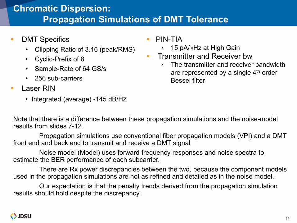
Chromatic Dispersion: Propagation Simulations of DMT Tolerance
Note that there is a difference between these propagation simulations and the noise-model results from slides 7-12. Propagation simulations use conventional fiber propagation models (VPI) and a DMT front end and back end to transmit and receive a DMT signal Noise model (Model) uses forward frequency responses and noise spectra to estimate the BER performance of each subcarrier. There are Rx power discrepancies between the two, because the component models used in the propagation simulations are not as refined and detailed as in the noise model. Our expectation is that the penalty trends derived from the propagation simulation results should hold despite the discrepancy.
DMT Specifics • Clipping Ratio of 3.16 (peak/RMS) • Cyclic-Prefix of 8 • Sample-Rate of 64 GS/s • 256 sub-carriers
Laser RIN • Integrated (average) -145 dB/Hz
PIN-TIA • 15 pA/√Hz at High Gain
Transmitter and Receiver bw • The transmitter and receiver bandwidth
are represented by a single 4th order Bessel filter

15
Penalty with 20 GHz Tx BW is < 1.0 dB for CWDM grid over 10 km With 25 GHz Tx, penalty is reduced to < 0.5 dB These simulated penalties are well below the proposed TDP value of 2.0 dB CD tolerance is low enough to consider the CWDM grid for 10km SMF
Chromatic Dispersion: Simulated BER vs Power, varying Tx BW
16
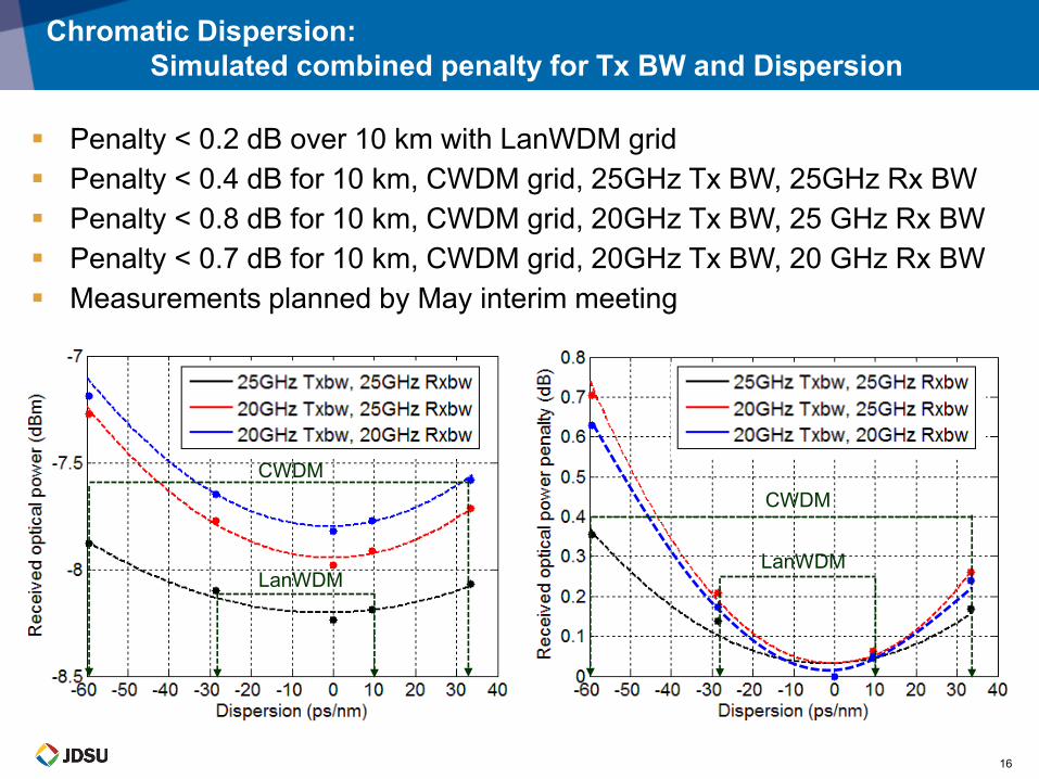
Chromatic Dispersion: Simulated combined penalty for Tx BW and Dispersion
Penalty < 0.2 dB over 10 km with LanWDM grid Penalty < 0.4 dB for 10 km, CWDM grid, 25GHz Tx BW, 25GHz Rx BW Penalty < 0.8 dB for 10 km, CWDM grid, 20GHz Tx BW, 25 GHz Rx BW Penalty < 0.7 dB for 10 km, CWDM grid, 20GHz Tx BW, 20 GHz Rx BW Measurements planned by May interim meeting
LanWDM
CWDM
LanWDM
CWDM
17
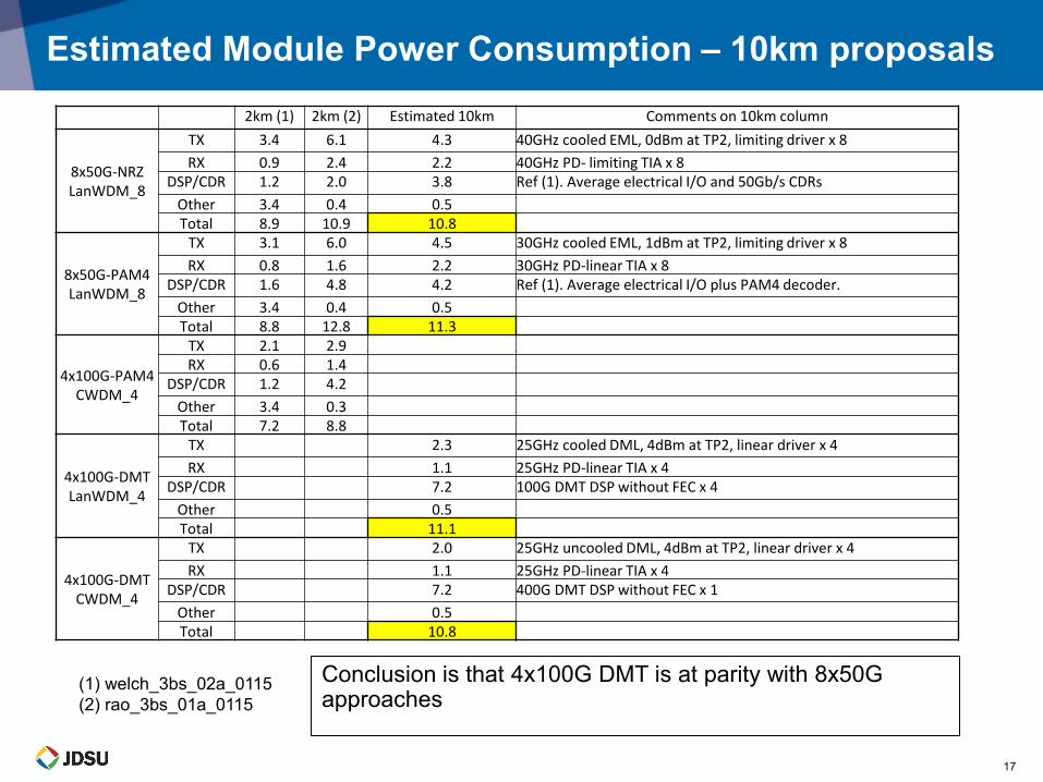
Conclusion is that 4x100G DMT is at parity with 8x50G approaches
Estimated Module Power Consumption – 10km proposals 2km (1) 2km (2) Estimated 10km Comments on 10km column
8x50G-NRZ LanWDM_8
TX 3.4 6.1 4.3 40GHz cooled EML, 0dBm at TP2, limiting driver x 8
RX 0.9 2.4 2.2 40GHz PD- limiting TIA x 8 DSP/CDR 1.2 2.0 3.8 Ref (1). Average electrical I/O and 50Gb/s CDRs
Other 3.4 0.4 0.5 Total 8.9 10.9 10.8
8x50G-PAM4 LanWDM_8
TX 3.1 6.0 4.5 30GHz cooled EML, 1dBm at TP2, limiting driver x 8
RX 0.8 1.6 2.2 30GHz PD-linear TIA x 8 DSP/CDR 1.6 4.8 4.2 Ref (1). Average electrical I/O plus PAM4 decoder.
Other 3.4 0.4 0.5 Total 8.8 12.8 11.3
4x100G-PAM4 CWDM_4
TX 2.1 2.9 RX 0.6 1.4
DSP/CDR 1.2 4.2
Other 3.4 0.3 Total 7.2 8.8
4x100G-DMT LanWDM_4
TX 2.3 25GHz cooled DML, 4dBm at TP2, linear driver x 4
RX 1.1 25GHz PD-linear TIA x 4 DSP/CDR 7.2 100G DMT DSP without FEC x 4
Other 0.5 Total 11.1
4x100G-DMT CWDM_4
TX 2.0 25GHz uncooled DML, 4dBm at TP2, linear driver x 4
RX 1.1 25GHz PD-linear TIA x 4 DSP/CDR 7.2 400G DMT DSP without FEC x 1
Other 0.5 Total 10.8
(1) welch_3bs_02a_0115 (2) rao_3bs_01a_0115

18
TX and RX for 4x100G is always the lowest cost due to: • 4-wide versus 8-wide • Similar bandwidth to 8x50G PAM4 but ~50% bandwidth of 8x50G NRZ
Total IC/non-optics cost for high volume modules tends to < 25% of total cost *
• Not able to estimate relative cost for ICs at this time * Based on experience at 10G/40G/100G pluggable modules
Estimated Module Relative Costs – 10km proposals
DMT PAM4 NRZ
4x100G 8x50G 8x50G
Optical MUX 1 1.2 1.2
DML/EML 1 2 2.5
Driver 1 2 2.5
Optical Demux 1 1.2 1.2
PD Array 1 1.5 1.5
TIA Array 1 1.5 2
DSP 1 - -
PAM/EncDec - 1 -
CDAUI Interface - - 1
TX
RX
IC

19
We propose to eliminate the BCH requirement and rely on KP4 FEC as for other proposals
The cascaded Tx and Rx bandwidths required (20 GHz) can be demonstrated now and is reasonable for volume production as 400GE starts to be implemented
CD penalty low and allows CWDM
Cost and power is advantageous for WDM and even better for CWDM • Using CWDM grid allows for reuse of 100G CWDM devices which
are already ramping towards high volume
Summary

20
Evaluate Coupling between electrical and optical interfaces
RX Technical feasibility
Dispersion penalty worst case
TDP. MPI
RX sensitivity
Optical loss budget model
Interoperability
Next Steps - BTIs
update by May interim
by May interim (measurements)
more measurements by May interim
tanaka_3bs_01a_0115 (measurements)
by May interim (measurements)
update at May interim
update at May interim

Thank You


![CHE COSA CHIAMIAMO REALTA'? - NEISHI · 2017. 11. 18. · Mimosa scabrella [DMT] Mucuna pruriens [DMT, 5MD] Petalostylis labicheoides var. casseoides [DMT] Malpighiaceae Banisteriopsis](https://static.fdocument.pub/doc/165x107/606c2e0710181960ef3fbf4a/che-cosa-chiamiamo-realta-neishi-2017-11-18-mimosa-scabrella-dmt-mucuna.jpg)


![[DMT]Ayahuasca Analoge Ott](https://static.fdocument.pub/doc/165x107/55cf9ba9550346d033a6e8dc/dmtayahuasca-analoge-ott.jpg)

