A large-area wireless power transmission sheet using ... · 1 Supplementary Information A...
16
1 Supplementary Information A large-area wireless power transmission sheet using printed organic transistors and plastic MEMS switches Tsuyoshi Sekitani 1 , Makoto Takamiya 2 , Yoshiaki Noguchi 1 , Shintaro Nakano 1 , Yusaku Kato 1 , Takayasu Sakurai 3 , and Takao Someya 1 * 1 Quantum-Phase Electronics Center, School of Engineering, The University of Tokyo, Tokyo 113-8656, Japan 2 VLSI Design and Education Center, The University of Tokyo, Tokyo 153-8505, Japan 3 Center for Collaborative Research, The University of Tokyo, Tokyo 153-8904, Japan Corresponding author: Takao Someya Quantum-phase Electronics Center School of Engineering, the University of Tokyo 7-3-1 Hongo, Bunkyo-ku, Tokyo 113-8656, JAPAN Telephone: +81-3-5841-6820, 6822 Fax: +81-3-5841-6828 E-mail: [email protected] © 2007 Nature Publishing Group
Transcript of A large-area wireless power transmission sheet using ... · 1 Supplementary Information A...
1
Supplementary Information
A large-area wireless power transmission sheet using printed organic
transistors and plastic MEMS switches
Tsuyoshi Sekitani1, Makoto Takamiya2, Yoshiaki Noguchi1, Shintaro Nakano1, Yusaku Kato1,
Takayasu Sakurai3, and Takao Someya1*
1 Quantum-Phase Electronics Center, School of Engineering, The University of Tokyo, Tokyo
113-8656, Japan
2 VLSI Design and Education Center, The University of Tokyo, Tokyo 153-8505, Japan
3 Center for Collaborative Research, The University of Tokyo, Tokyo 153-8904, Japan
Corresponding author: Takao Someya Quantum-phase Electronics Center School of Engineering, the University of Tokyo 7-3-1 Hongo, Bunkyo-ku, Tokyo 113-8656, JAPAN Telephone: +81-3-5841-6820, 6822 Fax: +81-3-5841-6828 E-mail: [email protected]
© 2007 Nature Publishing Group
2
1.Manufacturing process The entire system comprising an 8 × 8 array of cells is manufactured by integrating the position-sensing and power transmission sheets. The spacing of the cells is one inch (25.4 mm) for both the position-sensing unit and power transmission unit. The contactless position-sensing system comprises the position-sensing coil array sheet and an organic transistor active matrix sheet, as shown in Fig. S1a. The entire sheet area is 21 × 21 cm2 and includes 64 position-sensing units. Organic transistors are manufactured using inkjet, screen printing, and vacuum evaporation methods. The inkjet printing system (Ricoh Printing Systems Co., Ltd.; IJP-1) used in this study is equipped with two kinds of heads, one employs Ag nanoparticles and the other polyimide precursors The minimum line-width and spacing patterned using our inkjet are typically 60 μm and 60 μm, respectively, without surface treatments. The screen printing machine (Micro-tec Co. Ltd.; MT-550) can form line-width and spacing to be 20 μm and 20 μm, respectively. These performances are sufficiently-high for manufacturing electronic devices with microstructure. The base film (substrate) for organic transistors is a polyimide film with a thickness of 75 μm. Ag nanoparticles (Harima Chemical Co. Ltd.; NPS-J-HP) are patterned using inkjet and cured at 180 oC to form 300-nm-thick gate electrodes and word lines. When inkjetted Ag nanoparticles are cured at 180 °C, the resistivity of an electrode is 5.1 μΩcm, which is approximately 3 times larger than that of pure Ag (1.6 μΩcm). Epoxy partitions are formed around the gate electrodes using screen printing. Diluted polyimide precursors (Kyocera Chemical Co., Ltd.; KEMITITE CT4112) are inkjetted into the inside of epoxy partitions. Although the viscosity of diluted polyimide precursors is 11 mPa⋅s, it dose not spread out owing to epoxy partitions. Inkjetted polyimide precursors are cured at 180 °C to form 1-μm-thick polyimide gate dielectric layers. A 50-nm-thick pentacene layer and a 50-nm-thick gold layer are deposited using vacuum evaporation through shadow masks to form a channel layer and source and drain electrodes, respectively. Finally, an 8-μm-thick poly-chloro-para-xylylene, parylene (Daisankasei Co., Ltd.; diX-SR) is uniformly coated to form a passivation layer. Each via interconnection (through holes) is made using a CO2 laser. The diameter of through holes is approximately 100 μm. The fabrication process is similar to the method reported in ref. [Noguchi, Y., Sekitani, T. & Someya, T. Appl. Phys. Lett. 89, 253507 (2006)]. A position-sensing coil array is manufactured using screen printing and numerically controlled
© 2007 Nature Publishing Group
3
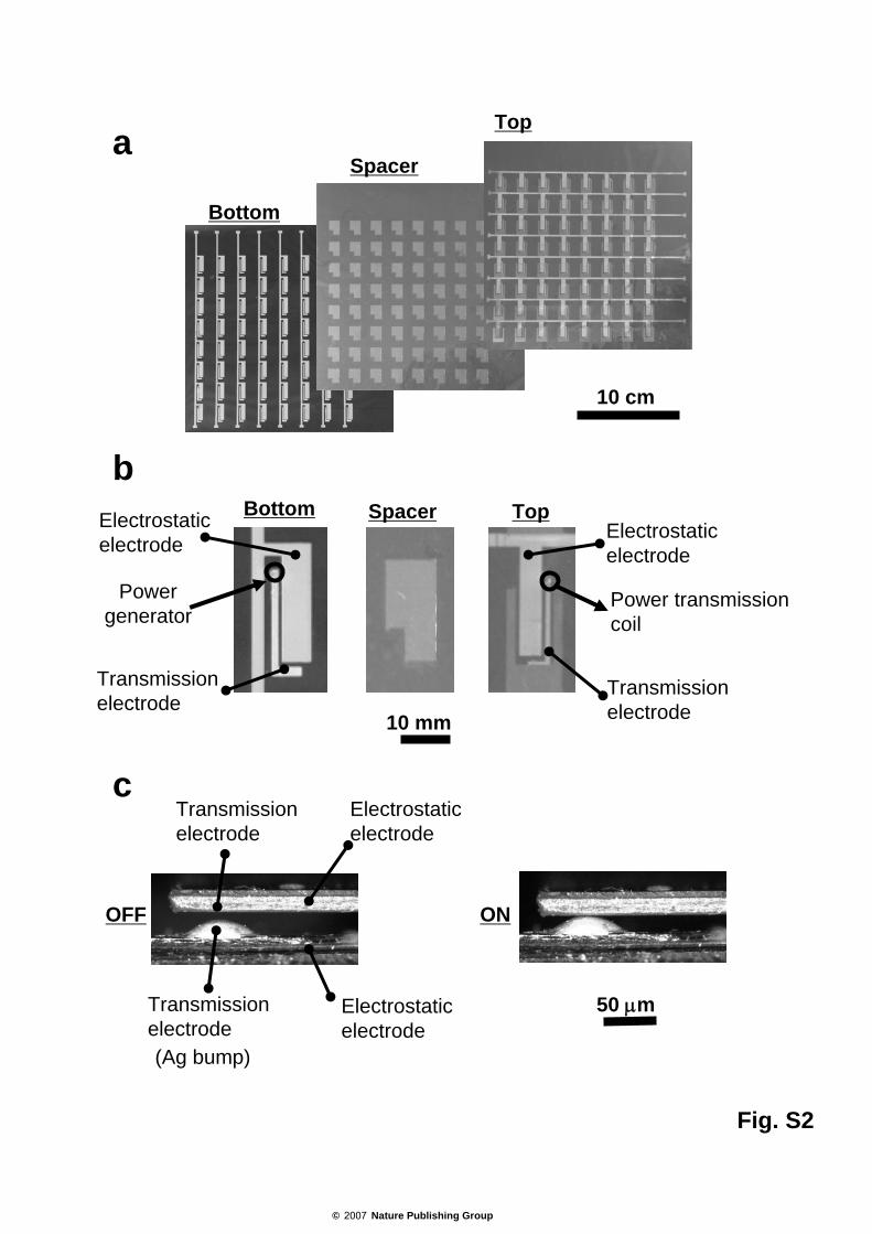
(NC) drilling machines. A polyimide film, with both surfaces coated with 20-μm-thick Cu, is covered with an etching-resist paste using a screen printing machine, and coils and bit lines are formed by etching using FeCl3 solution. Through holes with diameter of 300 μm are made using an NC drill machine and are plated with Ag solder to form interconnections between the bottom and top surfaces. The position-sensing coil array and the organic transistor active matrix sheet are interconnected using a Ag paste. The wireless power transmission sheet comprises the printed plastic micro-electrical-mechanical system (MEMS) switch sheet and sender coil array sheet, as shown in Fig. S1b. A MEMS switch matrix sheet is formed using inkjet printing and an NC cutting machine. An exploded view of the MEMS switch matrix sheet is shown in Fig. S2a. The electrodes for power transmission and those for electrostatic attraction are patterned on a polyimide membrane. The MEMS switch sheet is formed by the lamination of three plastic sheets. A 75-μm-thick polyimide film is used as the bottom sheet. First, through holes are made using a CO2 laser for interconnecting the top and bottom surfaces of the film, and 300-nm-thick Ag nanoparticles are inkjetted and cured to form electrodes for electrostatic attraction. The size of the stand-alone MEMS switch is 9 × 5 mm2. Subsequently, the sheet is coated with 3-μm-thick parylene, and 300-nm-thick Ag nanoparticles are inkjetted to form electrodes for power transmission. Finally, a 25-μm-thick Ag bump is placed at the edge of the electrodes for power transmission. A 25-μm-thick polyimide film is used as the middle sheet, which is a spacer fabricated using the NC cutter. A 25-μm-thick polyimide film is used as the top sheet; this is cut using the NC cutter to form movable rectangular arms and function as a cantilever. The fabrication process for the electrodes for power transmission and those for electrostatic attraction is the same as that for the bottom sheet. These sheets are laminated with adhesion films. The MEMS switch sheet has a periodicity of 25.4 mm and comprises an 8 × 8 array. The entire sheet size is 21 × 21 cm2. A magnified view and cross-sectional pictures of a stand-alone MEMS switch are shown in Figs. S2b, and c, respectively. A sender coil array sheet is also manufactured using screen printing and an NC drill. The manufacturing process for the coil array sheet is identical to that for the position-sensing coil array sheet. The inner and outer diameters of the sender coils are 10 mm and 25 mm, respectively. Both the width and spacing of the copper lines are 300 μm. The number of turns is 13. The inductance and resistance are 3 μH and 2 Ω, respectively. A sender coil array sheet and a plastic MEMS switch sheet are interconnected using a Ag paste.
© 2007 Nature Publishing Group
4
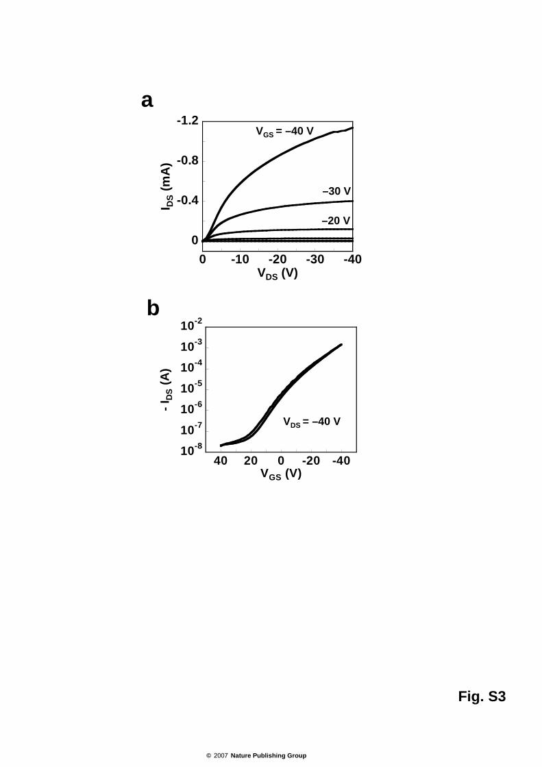
During the integration, the power transmission sheet is arranged above the position-sensing sheet where their center axes do not overlap and they are completely out of phase (Fig. S1c). This arrangement is important to avoid interference between the position sensing and power transmission operations. The distance between the position-sensing coil array sheet and the sender coil array sheet is 1 mm. 2. AC characteristics of organic transistors The typical transistor characteristics of the organic transistors were measured using a semiconductor parameter analyzer (4156C, Agilent technologies) immediately after exposure to ambient air. The pentacene transistors exhibited a mobility of 1 cm2/Vs and an on/off ratio of 105 in DC characterization, as shown in Fig. S3. The circuit of the position-sensing unit is formed by an integration of the organic transistor and position-sensing coil, as shown in Fig. S4a. An AC voltage of ±10 V at 2.95 MHz is applied to the position-sensing units. Figure S4b shows the sense voltages (VS) in the position-sensing unit with VGS = –60 V (on state) and VGS = 0 V (off state). The resonance voltage is detected at 2.95 MHz when there are no receiver coils. VS is less than 10 mV in the off state of the organic transistor. The on/off ratio of the transistors at 2.95 MHz exceeds 103. Such an excellent on/off ratio can be achieved at a high frequency because the capacitance between the source and drain electrodes is minimized to be less than 1 pF. The low resistance of the word and bit lines is crucial for reducing the fluctuation in the gate voltage. This design reduces the indirect capacitive coupling between the source and the drain electrodes through the gate electrodes. Figure S4c shows VS at the resonance frequency for a receiver coil approaching a position-sensing coil. The resonance frequency decreases with the closeness of approach of the receiver coil; as a result, VS at 2.95 MHz is significantly decreased as a receiver coil approaches. This is the principle of the contactless position-sensing system. 3. Plastic MEMS switches A stand-alone plastic MEMS switch is characterized as shown in Fig. S5. When a series of rectangular waves of amplitude 70 V (in the following referred to as operation voltage Vop) are applied to the electrodes for electrostatic attraction, the top electrodes for power transmission are mechanically connected with the power transmission electrodes on the bottom sheet due to the electrostatic attraction, thereby leading to a very low on-resistance and an excellent on/off ratio. In fact, the resistance changes from >106 Ω to 15 Ω by applying Vop. Such a low on-resistance is
© 2007 Nature Publishing Group
5
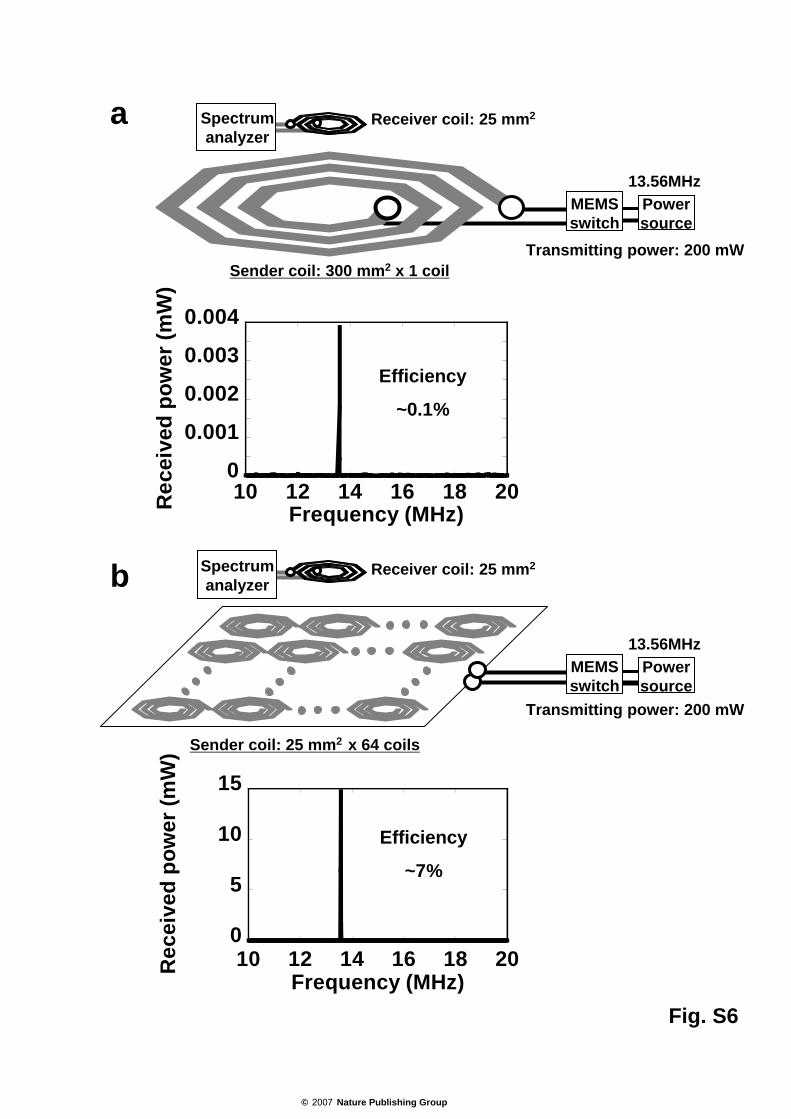
suitable for high power transmission (Fig. S5a). The response time for switch-on and switch-off of the MEMS switches depends on Vop (Fig. S5b), and the frequency response extends up to 4 Hz at Vop = 70 V. Vop of the MEMS switches also strongly depends on the distance between the top and the bottom sheets (Fig. S5c). A minimum Vop of less than 30 V can be achieved for a distance of approximately 5 μm. On the other hand, the resistance of the electric contact on the MEMS switches significantly increases with Vop decreases. Plastic films are inherently easy to deform; therefore, variations in Vop may be inevitable for plastic MEMS switches, particularly for their large-area switching matrices. The suppression of the deformation of plastic films using thermal and pressure processes is crucial for realizing reliable and stable plastic MEMS switch matrices. The fatigue durability of the MEMS switches is investigated as a function of the number of switching cycles, as shown in Fig. S5d. The change in the resistance of the contact point of the MEMS switch is less than 5% after 300,000 switching cycles when the MEMS switches are in a nitrogen environment. On the other hand, the resistance changes by more than 100% after 20,000 switching cycles when the MEMS switches are in air. This is because numerous switching cycles result in the oxidization of the Ag bumps that function as electric connections. In the case of organic transistors, many degradation processes are induced by oxygen- and moisture-associated atmospheric species, therefore, the stability of organic transistors is also a major concern. Encapsulation is effective in reducing the instability of the electrical characteristics of mechanical contact switches as well as organic transistors. 4. Power transmission efficiency without position-sensing units If the system does not contain a position-sensing unit, power transmission is possible; however, the power loss is huge. One of the straightforward means to transmit power without a position-sensing unit is to use a single large sender coil. We have prepared a 300 × 300 mm2 sender coil. When power is transmitted from this coil to a 25 × 25 mm2 receiver coil, the transmission efficiency is less than 0.1%, as shown in Fig. S6a. Another possible method to operate without a position-sensing unit is to activate all the sender coils. We prepared an 8 × 8 sender coil array in which the coils were electrically interconnected as a parallel circuit. When all the 64 sender coils were simultaneously activated to transmit an electric power of 200 mW to the receiver coil, the power received at the receiver coil was only 15 mW and the transmission efficiency was less than 7% (Fig. S6b). Therefore, selective power
© 2007 Nature Publishing Group

6
transmission is important to reduce power loss as mentioned in the text.
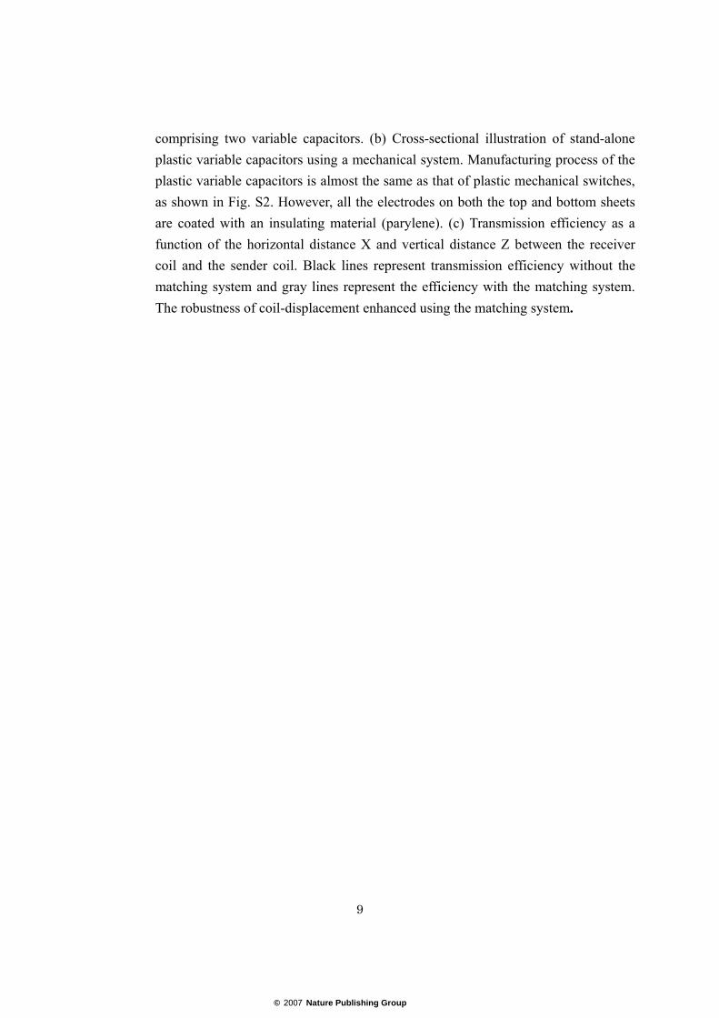
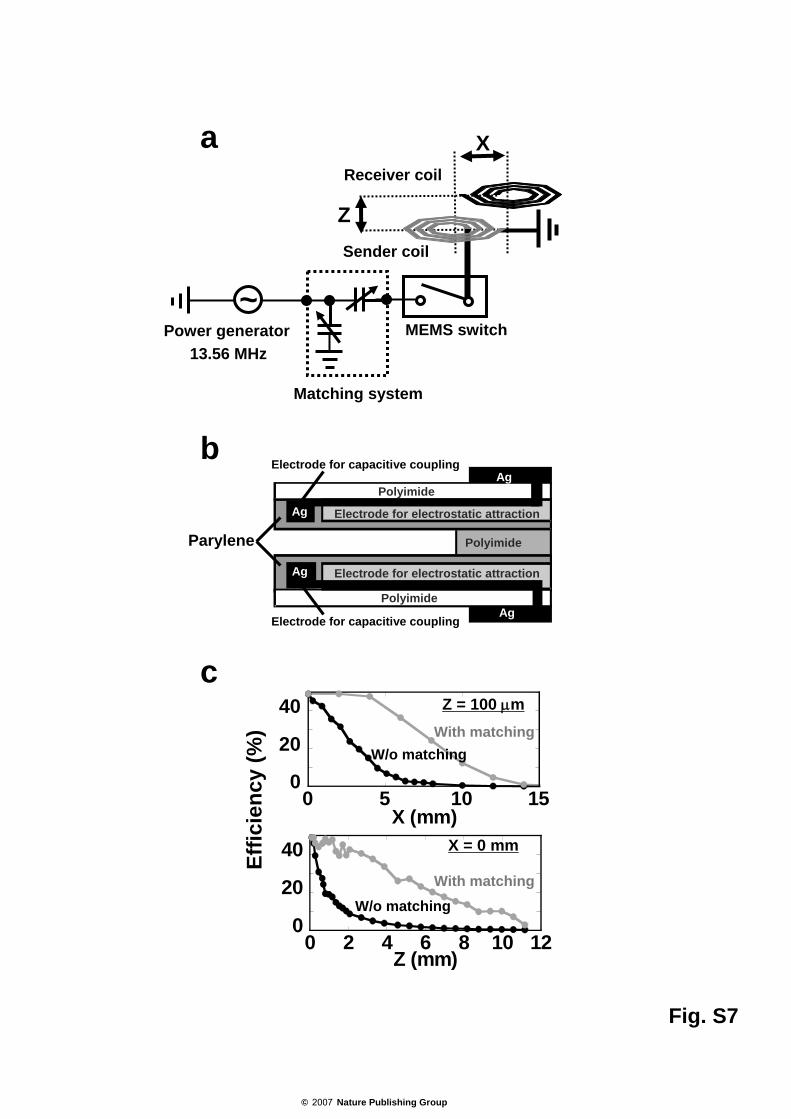
5. Robustness of coil displacement When the center axis of the receiver coil deviates from that of the sender coil, the power transmission efficiency decreases. In order to improve the robustness of coil displacement, a phase matching system using two variable capacitors is used, as shown in Fig. S7a. The cross-sectional illustration of a stand-alone variable capacitor is shown in Fig. S7b. The manufacturing process is similar to that of plastic MEMS switches, while all the electrodes of the variable capacitors are coated with an insulating material (parylene). The principle of operation of plastic variable capacitors is quite similar to that of plastic MEMS switches, namely, the capacitance increases with the voltage bias applied to the electrodes for the electrostatic attraction because the electrodes involved in the capacitive coupling approach each other. The matching system can adjust reflection of the power to the transmission. Figure S7c shows the transmission efficiency as a function of the horizontal distance (X) and vertical distance (Z) between the receiver coil and the sender coil. The transmission efficiency decreases with an increase in the coil displacement. The black lines represent the transmission efficiency without the matching system and the gray lines represent the efficiency with the matching system. In fact, the robustness of the coil displacement improves when the matching system is used. 6. Transmission efficiency One of the concerns could be the electromagnetic interference between the position-sensing coils and the sender coils. However, the sender coils and the position-sensing coils are arranged so that their center axes do not overlap and thereby they are completely out of phase. In fact, the transmission efficiency between the sender coil and the position-sensing coil is less than 0.1% and almost the entire electric power is transmitted to the receiver coils. Although the transmission efficiency in our power transmission system exceeds 80%, such a high efficiency can be achieved using power transmission electrodes with three times recoating of inkjetted Ag nanoparticles. In fact, the present efficiency is mainly determined by the resistance of the circuit (less than 10 Ω), which leads to heat generation. For example, the maximum transmission efficiency is as high as 62.3% when power transmission electrodes are formed with one or two times recoating of Ag nanoparticles. Furthermore, there is considerable space to reduce the resistance by optimizing the device structures and manufacturing process. Although present sender coils and receiver coils are designed for achieving high transmission efficiency, much further design of the receiver coils is required to improve the power transmission efficiency.
© 2007 Nature Publishing Group

7
Figure captions Figure S1: Illustration of the contactless position-sensing sheet and wireless power transmission
sheet and their relative orientations. (a) Picture of the contactless position-sensing sheet comprising a position-sensing coil array sheet and an organic transistor sheet. (b) Picture of the wireless power transmission sheet comprising a sender coil array sheet and a plastic MEMS switch sheet. Size of these sheets is 21 × 21 cm2. (c) Integration of the power transmission sheet and position-sensing sheet. The former is arranged above the latter, and the sender coils and position-sensing coils are arranged so that their center axes do not overlap and they are completely out of phase. The distance between the two sheets is 1 mm. On the other hand, the distance between the sender coils and the receiver coils is set at 100 μm for high transmission efficiency.
Figure S2: Schematic of the MEMS switch matrix sheet and stand-alone MEMS switch. (a)
Exploded view of a plastic MEMS switch matrix sheet comprising three sheets: the bottom sheet (75-μm-thick polyimide), spacer (25-μm-thick polyimide), and top sheet (25-μm-thick polyimide). The plastic MEMS switch sheet is formed by the lamination of the three plastic sheets using a Ag paste. (b) Magnified pictures of a stand-alone MEMS switch. The electrodes for power transmission and those for electrostatic attraction are formed using inkjetted Ag nanoparticles. A 25-μm-thick polyimide film is used as the top sheet, which is cut using an NC cutter to form movable rectangular arms that function as a cantilever. The spacer sheet is also formed using the NC cutter. Through holes are made using a CO2 laser for interconnecting the top and bottom surfaces of the film. (c) Cross-sectional pictures of a stand-alone MEMS switch; a voltage bias of 0 V is applied to the electrode for electrostatic attraction (off state) following which a bias of 70 V is applied (on state).
Figure S3: Organic (pentacene) transistor characteristics. (a) Transistor characteristics of an
organic transistor. The channel length and width are 13 μm and 48 mm, respectively. Source-drain current (IDS) is monitored as a function of the source-drain voltage (VDS) when the gate voltage (VGS) is changed from 0 to –40 V in steps of 10 V. (b) The transfer characteristics of the same organic transistor—VGS was swept from 0 to –40 V with the application of VDS = –40 V.
Figure S4: Voltage-frequency characteristics of the contactless position-sensing unit. (a) Circuit
© 2007 Nature Publishing Group

8
diagram of a contactless position-sensing unit comprising an organic transistor and a position-sensing coil. A voltage of ±10 V is applied to the organic transistor, which is connected to a position-sensing coil and detector. Capacitance and inductance are chosen to resonate the circuit at around 3 MHz. (b) Sense voltages (VS) in the position-sensing unit as a function of the frequency with VGS = 0 V and –60 V, where a voltage of ±10 V is applied to the drain electrode of the organic transistor. Resonance voltage is observed at the frequency (fR) of 2.95 MHz. (c) Magnified view of the resonance frequency as a receiver coil approaches the position-sensing coil. VS in the position-sensing unit with VGS of –60 V when a receiver coil approaches the position-sensing coil. Resonance frequency decreases with the closeness of approach of the receiver coil, leading to a decrease in VS.
Figure S5: MEMS switch resistance and Vop characteristics. (a) Resistance of a stand-alone
plastic MEMS switch as a function of time. When a rectangular wave with a Vop of 70 V is applied to the MEMS switch, the resistance changes from >106 Ω to 15 Ω. (b) Response time of the stand-alone MEMS switch as a function of Vop. “switch-on” and “switch-off” represent the times of change in the resistance from >106 Ω to 15 Ω and from 15 Ω to >106 Ω, respectively. (c) Vop as a function of the distance between the top and the bottom sheet. (d) Resistance of the MEMS switch as a function of the number of switching cycles. Measurements are performed in air (square) and in a nitrogen environment (circle). Vop is 70 V.
Figure S6: Power-frequency characteristics. (a) Transmission efficiency as a function of
frequency in the circuit where electric power is transmitted from a large sender coil to the receiver coil. An electric power of 200 mW is transmitted from the sender coil to the receiver coil. The inner and outer diameters of the receiver coil are 10 mm and 25 mm, respectively, while the inner and outer diameters of the sender coil are 100 mm and 300 mm, respectively. (b) Transmission efficiency as a function of the frequency in the circuit where electric power is transmitted from 64 sender coils to a single receiver coil. The inner and outer diameters of the receiver coil are 10 mm and 25 mm, respectively, and the size of a sender coil is the same as that of the receiver coil. On the other hand, all the 64 sender coils are electrically interconnected as a parallel circuit.
Figure S7: Matching system and coil-displacement on wireless power transmission unit. (a)
Schematic illustration of wireless power transmission unit using a matching system
© 2007 Nature Publishing Group
9
comprising two variable capacitors. (b) Cross-sectional illustration of stand-alone plastic variable capacitors using a mechanical system. Manufacturing process of the plastic variable capacitors is almost the same as that of plastic mechanical switches, as shown in Fig. S2. However, all the electrodes on both the top and bottom sheets are coated with an insulating material (parylene). (c) Transmission efficiency as a function of the horizontal distance X and vertical distance Z between the receiver coil and the sender coil. Black lines represent transmission efficiency without the matching system and gray lines represent the efficiency with the matching system. The robustness of coil-displacement enhanced using the matching system.
© 2007 Nature Publishing Group

Organic transistor sheet
Position-sensing coil sheet
Contactless position-sensing system
MEMS switch sheet
Wireless power transmission system
Sender coil sheet
a
b
Position-sensing coil sheet
Sender coil sheet
Z =100 μm
1 mm
Receiver coil
cPosition-sensing coil sheet
Sender coil sheet
Fig. S1
© 2007 Nature Publishing Group
Electrostatic electrode
a
b
10 cm
Top SpacerBottom Electrostatic electrode
Transmission electrode
Transmission electrode
Power transmission coil
Electrostatic electrode
10 mm
Bottom
Spacer
Top
Power generator
c
ON
(Ag bump)
50 μm
OFF
Transmission electrode
Transmission electrode
Electrostatic electrode
Fig. S2
© 2007 Nature Publishing Group
10-810-7
10-610-510-410-3
10-2
-40-2002040
- ID
S (A
)
VGS (V)
-1.2
-0.8
-0.4
0-40-30-20-100
I DS
(mA
)
VDS (V)
VDS = –40 V
a
b
VGS = –40 V
–30 V
–20 V
Fig. S3
© 2007 Nature Publishing Group

02468
10
100 102 104 106 108
V S (V
)
Frequency (Hz)
a
(b)
~
300 pF 300 pF
20 μH
10 MΩ
550 pF
Transistor
Detector
0
2
4
6
2.7 2.8 2.9
V S (V
)
Frequency (MHz)
cWith approaching receiver coil
Transistor on
10 VPosition-sensing coil
Resonance
peak
VGS = 0 V
b
VGS = –60 V
(VGS = –60 V)
(VGS = –60 V)
Fig. S4
© 2007 Nature Publishing Group

0
100
200
300
400
500
0 20 40 60 80 100 120
V op
(V)
d (μm)
R (Ω
)V op
(V)
Time (s)
80
40
0>106
8040
0 0 5 10 15 20
0
20
40
60
80
100
103 104 105 106
R (Ω
)
Number of switching cycles
In air
In nitrogen
a
c
0
0.1
0.2
0.3
70 80 90 100 110 120 130R
espo
nse
time
(s)
Vop (V)
Switch-on
Switch-off
b
d
d
Fig. S5
© 2007 Nature Publishing Group
a
13.56MHzMEMS switch
Power source
Transmitting power: 200 mW
Receiver coil: 25 mm2
Sender coil: 300 mm2 x 1 coil
0
0.001
0.002
0.003
0.004
10 12 14 16 18 20Rec
eive
d po
wer
(mW
)
Frequency (MHz)
Efficiency
~0.1%
0
5
10
15
10 12 14 16 18 20Rec
eive
d po
wer
(mW
)
Frequency (MHz)
Efficiency
~7%
b
13.56MHzMEMS switch
Power source
Spectrum analyzer
Sender coil: 25 mm2 x 64 coils
Receiver coil: 25 mm2
Spectrum analyzer
Transmitting power: 200 mW
Fig. S6
© 2007 Nature Publishing Group
a
0
20
40
0 5 10 15X (mm)
0
20
40
0 2 4 6 8 10 12Z (mm)
With matchingW/o matching
With matchingW/o matching
Effic
ienc
y (%
)
X = 0 mm
Z = 100 μm
X
Matching system
c
b
Parylene
PolyimideAg
Polyimide
Ag
Ag
AgPolyimide
Electrode for electrostatic attraction
Electrode for electrostatic attraction
Electrode for capacitive coupling
Electrode for capacitive coupling
ZSender coil
Receiver coil
13.56 MHzPower generator MEMS switch
~~
Fig. S7
© 2007 Nature Publishing Group