A 40–50-GHz SiGe 1 : 8 Differential Power Divider Using Shielded Broadside-Coupled Striplines
7
IEEE TRANSACTIONS ON MICROWAVE THEORY AND TECHNIQUES, VOL. 56, NO. 7, JULY 2008 1575 A 40–50-GHz SiGe 1 : 8 Differential Power Divider Using Shielded Broadside-Coupled Striplines Jason W. May, Student Member, IEEE, and Gabriel M. Rebeiz, Fellow, IEEE Abstract—This paper presents a 1 : 8 differential power divider implemented in a commercial SiGe BiCMOS process using fully shielded broadside-coupled striplines integrated vertically in the silicon interconnect stackup. The 1 : 8 power divider is only 1.12 1.5 mm including pads, and shows 0.4-dB rms gain im- balance and 3 rms phase imbalance from 40 to 50 GHz over all eight channels, a measured power gain of 14.9 0.6 dB versus a passive divider at 45 GHz, and a 3-dB bandwidth from 37 to 52 GHz. A detailed characterization of the shielded broadside-cou- pled striplines is presented and agrees well with simulations. These compact lines can be used for a variety of applications in SiGe/CMOS millimeter-wave circuits, including differential signal distribution, miniature power dividers, matching networks, filters, couplers, and baluns. Index Terms—BiCMOS, differential power divider, RF inte- grated circuit (RFIC), shielded broadside-coupled striplines, SiGe. I. INTRODUCTION T RADITIONAL RF-based phased arrays require an RF distribution network to divide the input power equally in amplitude and phase to the different radiating elements. The divider network should also result in high isolation between the elements and a good impedance match at each port. This is usually done using Wilkinson couplers on low dielectric constant substrates, and a 1 : 8 or a 1 : 16 network can be easily fabricated using three or four stages [1]. However, such a power divider is very large for RF integrated circuit (RFIC) applications and can be more compactly implemented using active techniques. Recently, a 1 : 16 SiGe active single-ended distribution network was demonstrated at 32–38 GHz with excellent phase and amplitude balance [2]. The 1 : 16 divider was based on microstrip lines and cascaded active 1 : 4 power dividers. This paper presents a differential 1 : 8 power divider based on a novel fully shielded broadside-coupled strip (BCS) line topology integrated into the silicon RFIC back-end. The BCS lines allow the integration of miniature 1 : 4 passive dividers without any crossovers, and result in a 1 : 8 divider with ex- cellent phase and amplitude balance at 40–50 GHz. Recently, asymmetric BCS lines have been used in a 0.18- m CMOS Manuscript received January 1, 2008; revised March 24, 2008. First pub- lished May 23, 2008; last published July 9, 2008 (projected). This work was supported by the Defense Advanced Research Projects Agency (DARPA) under the SMART Program under a subcontract from the Teledyne Scien- tific Corporation. The authors are with the Electrical and Computer Engineering Department, University of California at San Diego, La Jolla, CA 92093-0407 USA (e-mail: [email protected]; [email protected]). Color versions of one or more of the figures in this paper are available online at http://ieeexplore.ieee.org. Digital Object Identifier 10.1109/TMTT.2008.924363 Fig. 1. Differential passive 1 : 4 power-divider network. Broadside-coupled transmission lines eliminate crossovers present in a coplanar differential power divider. process for a low-loss balun [3], and symmetric lines are used in [4] for a partly shielded balun, but these incompletely shielded implementations are not optimal for densely packed power dividers. Other power dividers include the uniplanar monolithic microwave integrated circuit (MMIC) structure [5], [6] and transformer-based dividers [7]. These dividers, however, are more suited for 1 : 2 power dividers and would occupy large areas for 1 : 4 and 1 : 8 power dividers. Section II presents design equations and measurements of millimeter-wave BCS lines on silicon substrates together with a detailed transition between the BCS and coplanar lines. Section III discusses the 1 : 8 power divider in detail. The power-divider measurements are then presented in Section IV. This paper concludes with a discussion of the measured results and future applications of this technology. II. BROADSIDE-COUPLED TRANSMISSION LINES A. Analysis Millimeter-wave integrated circuits (ICs) commonly use variants of the coplanar waveguide (CPW) line for differential transmission lines [8], [9]. However, CPW transmission lines present difficulties when used in differential passive power division networks (Fig. 1). A differential CPW-line divider has several crossovers, which affect the divider isolation and symmetry. These crossovers are removed with the use of a BCS structure built vertically in the RFIC process back-end. 0018-9480/$25.00 © 2008 IEEE
Transcript of A 40–50-GHz SiGe 1 : 8 Differential Power Divider Using Shielded Broadside-Coupled Striplines

IEEE TRANSACTIONS ON MICROWAVE THEORY AND TECHNIQUES, VOL. 56, NO. 7, JULY 2008 1575
A 40–50-GHz SiGe 1 : 8 Differential Power DividerUsing Shielded Broadside-Coupled Striplines
Jason W. May, Student Member, IEEE, and Gabriel M. Rebeiz, Fellow, IEEE
Abstract—This paper presents a 1 : 8 differential power dividerimplemented in a commercial SiGe BiCMOS process using fullyshielded broadside-coupled striplines integrated vertically inthe silicon interconnect stackup. The 1 : 8 power divider is only1.12 1.5 mm2 including pads, and shows 0.4-dB rms gain im-balance and 3 rms phase imbalance from 40 to 50 GHz overall eight channels, a measured power gain of 14.9 0.6 dB versusa passive divider at 45 GHz, and a 3-dB bandwidth from 37 to52 GHz. A detailed characterization of the shielded broadside-cou-pled striplines is presented and agrees well with simulations.These compact lines can be used for a variety of applications inSiGe/CMOS millimeter-wave circuits, including differential signaldistribution, miniature power dividers, matching networks, filters,couplers, and baluns.
Index Terms—BiCMOS, differential power divider, RF inte-grated circuit (RFIC), shielded broadside-coupled striplines, SiGe.
I. INTRODUCTION
T RADITIONAL RF-based phased arrays require an RFdistribution network to divide the input power equally in
amplitude and phase to the different radiating elements. Thedivider network should also result in high isolation betweenthe elements and a good impedance match at each port. Thisis usually done using Wilkinson couplers on low dielectricconstant substrates, and a 1 : 8 or a 1 : 16 network can be easilyfabricated using three or four stages [1]. However, such apower divider is very large for RF integrated circuit (RFIC)applications and can be more compactly implemented usingactive techniques. Recently, a 1 : 16 SiGe active single-endeddistribution network was demonstrated at 32–38 GHz withexcellent phase and amplitude balance [2]. The 1 : 16 dividerwas based on microstrip lines and cascaded active 1 : 4 powerdividers.
This paper presents a differential 1 : 8 power divider basedon a novel fully shielded broadside-coupled strip (BCS) linetopology integrated into the silicon RFIC back-end. The BCSlines allow the integration of miniature 1 : 4 passive dividerswithout any crossovers, and result in a 1 : 8 divider with ex-cellent phase and amplitude balance at 40–50 GHz. Recently,asymmetric BCS lines have been used in a 0.18- m CMOS
Manuscript received January 1, 2008; revised March 24, 2008. First pub-lished May 23, 2008; last published July 9, 2008 (projected). This work wassupported by the Defense Advanced Research Projects Agency (DARPA)under the SMART Program under a subcontract from the Teledyne Scien-tific Corporation.
The authors are with the Electrical and Computer Engineering Department,University of California at San Diego, La Jolla, CA 92093-0407 USA (e-mail:[email protected]; [email protected]).
Color versions of one or more of the figures in this paper are available onlineat http://ieeexplore.ieee.org.
Digital Object Identifier 10.1109/TMTT.2008.924363
Fig. 1. Differential passive 1 : 4 power-divider network. Broadside-coupledtransmission lines eliminate crossovers present in a coplanar differential powerdivider.
process for a low-loss balun [3], and symmetric lines are used in[4] for a partly shielded balun, but these incompletely shieldedimplementations are not optimal for densely packed powerdividers. Other power dividers include the uniplanar monolithicmicrowave integrated circuit (MMIC) structure [5], [6] andtransformer-based dividers [7]. These dividers, however, aremore suited for 1 : 2 power dividers and would occupy largeareas for 1 : 4 and 1 : 8 power dividers. Section II presentsdesign equations and measurements of millimeter-wave BCSlines on silicon substrates together with a detailed transitionbetween the BCS and coplanar lines. Section III discusses the1 : 8 power divider in detail. The power-divider measurementsare then presented in Section IV. This paper concludes with adiscussion of the measured results and future applications ofthis technology.
II. BROADSIDE-COUPLED TRANSMISSION LINES
A. Analysis
Millimeter-wave integrated circuits (ICs) commonly usevariants of the coplanar waveguide (CPW) line for differentialtransmission lines [8], [9]. However, CPW transmission linespresent difficulties when used in differential passive powerdivision networks (Fig. 1). A differential CPW-line dividerhas several crossovers, which affect the divider isolation andsymmetry. These crossovers are removed with the use of aBCS structure built vertically in the RFIC process back-end.
0018-9480/$25.00 © 2008 IEEE

1576 IEEE TRANSACTIONS ON MICROWAVE THEORY AND TECHNIQUES, VOL. 56, NO. 7, JULY 2008
Fig. 2. Even- and odd-mode impedances versus linewidth for symmetricalbroadside-coupled lines, simulated with Sonnet (t = 1:765 �m).
Broadside differential lines generally require less horizontalspace than coplanar lines, and the isolation between adjacentlines is achieved by using a layer of vias between two differentlines, resulting in a shielded BCS on silicon substrates.
Fig. 2 presents a cross section of a BCS line and calculatedimpedances for varying linewidths. The even- and odd-modeimpedances for shielded broadside-coupled lines with zerothickness are given by (1) as follows:
(1)
where is the vertical spacing between ground planes, is thesignal line spacing, is the signal linewidth, parameterrelated to and , and andare complete elliptic integrals of the first kind [10]. Valuesfor versus have been tabulated in [11], and athickness correction term can be applied for nonzero thicknessconductors [12]. The impedances for varying line geometriesare obtained using several software packages [13], [14] and areshown in Fig. 2 for various linewidths. In this case, the even-and odd-mode impedances refer to the impedance of a singlecoupled line. The differential-mode impedance is obtained bydriving the two coupled lines differentially and is .Similarly, the common-mode impedance is obtained by drivingboth lines with the same signal, and is .
Two shielded BCS structures were designed in the inter-connect layers in the Jazz Semiconductor SiGe BiCMOSSBC18HX process (Fig. 3). The process geometries do notpermit a perfectly symmetrical strip line structure, but a closeapproximation is obtained by connecting the two lower metallayers with vias. Shielding vias are also placed 5 m from thesignal lines to completely enclose the broadside-coupled lines.This distance was determined using full-wave simulations(Sonnet), and by increasing the shielding via distance until afurther increase resulted in negligible changes in the differen-tial-mode line characteristics. The electric field distributions forthe common and differential modes are shown in Fig. 4 [15].
Fig. 3. Shielded broadside-coupled transmission lines (2- and 4-�m wide) builtvertically in the Jazz Semiconductor SBC18HX process. A nearly symmetricstructure is created by connecting two lower levels with vias. All dimensionsare in micrometers.
Fig. 4. HFSS simulation field plots of the: (a) common- and (b) differential-mode field distribution for a 2-�m-wide strip line.
Note that when used differentially, the electric field is tightlycoupled between the two signal lines with very low coupling tothe top and bottom metal layers and negligible coupling to theside shielding vias.
It is well known that geometrical line asymmetries generateundesired mode conversions (differential to common mode andvice versa), and this can be examined by converting the four-port single-ended scattering parameters to mixed-mode scat-tering parameters using the following matrix transformation in(2) [16], [17]:
(2)
(3)
The terms and indicate undesired cross-mode cou-pling and are ideally zero for a symmetric structure, and theand terms are the differential- and common-mode -param-eters, respectively. The differential- and common-mode imped-ances can be calculated using the and terms with a con-ventional two-port impedance calculation, as in [18].
The simulated impedances for the even and odd modes agreewell with the symmetric-line impedances in Fig. 2, and the sim-ulated loss is 1 dB/mm at 20 GHz. The lines are sufficiently

MAY AND REBEIZ: 40–50-GHz SiGe 1 : 8 DIFFERENTIAL POWER DIVIDER USING SHIELDED BROADSIDE-COUPLED STRIPLINES 1577
Fig. 5. Fabricated transmission line test structure and deembedding of pad tran-sition effects using electromagnetic (EM) simulated models and chain matrices.
Fig. 6. Transition from the GSSG pads to the shielded BCS lines. The left andright sidewall vias are depicted as a solid layer of metal for clarity.
symmetric to maintain mode conversion terms below 32 dBat 45 GHz for 500- m lines. A dielectric permittivity of 4.2 isused for simulations, as indicated by the Jazz SemiconductorDesign Manual, and metal resistivities are calculated from thesheet metal resistances and thicknesses in the manual [19]. Adielectric loss tangent from 0.01 to 0.07 is used for SiO in aCMOS process [20]. The via resistance is taken to be 10 /con-tact as described in the Jazz Semiconductor Design Manual.
B. Broadside Coupled Stripline Measurements
Shielded BCS lines were fabricated in the Jazz Semicon-ductor 0.18- m SiGe BiCMOS process (SBC18HX) with2- m width and 1150- m length. The test structure connects to100- m pitch pads and ground–signal–signal–ground (GSSG)probes (Fig. 5). Two short (37 m) single-ended line sectionson metal layer M5 transition from the signal pads to the differ-ential structure, where one of the signal lines descends to M4and M3 (Fig. 6). A compact test layout is achieved using bendsin the BCS line, as shown in Fig. 5.
Measurements were done with an Agilent 10-MHz–50-GHzfour-port network analyzer (E8364B), and calibrated to theprobe tips using a Cascade 129–246 impedance standard sub-strate. Sonnet chain-matrix models of the GSSG pads, 37- mlines, and transitions were used to estimate and deembed theeffects of the pads/transitions, which accounted for roughly85-pH series inductance and 12-fF shunt capacitance (Fig. 5).
Fig. 7. Measured and simulated impedances of 2-�m-wide shielded BCS lines.
Fig. 8. Insertion loss per 500-�m line length, and differential-to-common-mode conversion for the 2-�m shielded BCS lines.
The GSSG to shielded BCS transition is nearly ideal and thesimulated mode-conversion terms using Sonnet are 49 dBat 1–50 GHz.
The measured differential -parameters and thecommon-mode -parameters result in a differential-and common-mode impedances from 67 to 71 and 26 to32 , respectively, from 5 to 26 GHz and agree well withsimulations (Fig. 7). Impedance calculations below 5 GHzare made difficult by the short line length, and the crosstalkbetween adjacent fingers of the 100- m GSSG probes degradedthe measurement accuracy above 26 GHz (“partially leaky”calibration algorithms and calibration structures have beenrecently presented that address this crosstalk [21], but werenot implemented with this measurement). The measured modeconversion terms and are 30 dB from 5 to 26 GHz(Fig. 8). The measured loss is higher than modeled (2 dB versus1 dB at 26 GHz for a 500- m line length), and may be due toun-modeled line roughness and its effect on the high electricfield between M4 and M5 in the differential mode (see Fig. 4).We are currently investigating this additional loss using BCSlines with different widths and lengths.

1578 IEEE TRANSACTIONS ON MICROWAVE THEORY AND TECHNIQUES, VOL. 56, NO. 7, JULY 2008
Fig. 9. Differential 1 : 8 power-divider system topology. DTS amplifiers areadded at each output port to facilitate testing.
III. 1 : 8 POWER-DIVIDER DESIGN AND MEASUREMENTS
A. System Architecture
The 1 : 8 power divider is designed to be integrated in a dif-ferential RF phase-shifting transmit system with a single-endedinput and eight differential outputs (Fig. 9). A differentialtopology is chosen to reduce substrate coupling between thechannels and between the input and output ports. The inputstage is a combined single-ended to differential converter and1 : 2 power divider. This is followed by two miniature passive1 : 4 power dividers implemented using shielded BCS lines.The 1 : 4 dividers are then followed by standard differentialamplifiers, and the use of compact matching stubs in the 1 : 4BCS power-divider networks removes the need for lumpedmatching inductors at the inputs of the differential amplifiers.Differential to single-ended (DTS) output buffers based onthe push–pull design are added at the output ports to facilitatetesting.
B. Miniature Passive 1 : 4 Power Divider
The passive 1 : 4 power divider and the correspondingmatching network are shown in Figs. 10 and 11. The networkis designed for a conjugate match to the differential amplifierinput impedance ), which includes the ef-fect of the transition from BCS lines to the coplanar decouplingcapacitors at the amplifier input (note that, in this section, allimpedances are differential-mode impedances). The length andcharacteristic impedance of line mare chosen to tune out the capacitive portion of using ashunt inductor ( pH at 45 GHz). At node B, two shuntinductors are required to match two different amplifiers, andtheir parallel shunt inductance is 130 pH. This is synthesizedusing a short-circuited stub with mat node B. The impedance seen at is 37 , and ischosen to be close to so as to minimize the effect of line
. The impedance seen at , then, is ideally18 , and can be matched to 100 using line and a shuntdifferential capacitor.
The miniature passive 1 : 4 power divider has a total length of880 m ( m at 45 GHz) primarily determined bythe amplifier and output pad spacing, and compactly integratesall matching stubs and capacitors in an area of 78 912 m
Fig. 10. (a) Layout of 1 : 4 differential passive power-divider network (onlytwo of four output amplifiers shown). (b) Schematic (impedances are differentialmode).
Fig. 11. Smith chart (100- differential, 40–50 GHz) for the 1 : 4 passivepower-divider impedances shown in Fig. 10.
(0.071 mm ). A disadvantage of using high-impedance broad-side coupled lines is that their small size increases the seriesresistance—in this case, with 380- m line length and0.05- /sq sheet resistivity results in around 9.5 of seriesresistance. Based on the measured line loss in Fig. 8, the BCSline loss at 45 GHz is extrapolated to 3.2 dB/500 m for the2- m-wide line, and the 1 : 4 power-divider loss is estimated tobe 3.2–3.5 dB above the standard 6-dB split loss.
C. Active Circuit Design
The input single-ended to differential converter is a standarddifferential amplifier with one input grounded and a 1 : 2 cur-

MAY AND REBEIZ: 40–50-GHz SiGe 1 : 8 DIFFERENTIAL POWER DIVIDER USING SHIELDED BROADSIDE-COUPLED STRIPLINES 1579
Fig. 12. (a) Input 1 : 2 single-ended to differential converter. (b) Differential amplifier used at the output of the passive 1 : 4 power divider. (c) Output DTSpush–pull amplifier.
rent divider at the cascode node [see Fig. 12(a)]. The input portis matched to 50 at 31–60 GHz ( dB) using ashort 50- CPW line and a grounded 70- inductive matchingstub ( pH, at 45 GHz). The input de-vices are sized so that an emitter inductor is not needed for theinput match, and are biased near their peak . The 400-fF se-ries capacitor is composed of four 100-fF capacitors in parallelto increase the self-resonant frequency. Two single-ended in-ductors (200 pH, at 45 GHz) are used at the amplifiercollector in place of a differential inductor to simplify layout.The collector output is matched to 100 to simplify the designof the passive 1 : 4 BCS power divider ( dB from40 to 55 GHz). A 15- resistor in series with the inductor re-duces the and increases the match bandwidth. The transistorsare biased using simple current mirrors and resistors/diodes areused to set the cascode voltages. The single-ended to differentialconverter has a simulated single-channel power gain of 4.5 dBat 45 GHz, which includes the 3-dB power split loss from 1 : 2power division and 3-dB loss from grounding one side of thedifferential pair The simulated common-mode output is 22 dBbelow the differential output signal.
Inductively loaded differential amplifiers follow the passive1 : 4 BCS power-divider network [see (Fig. 12(b)]. These ampli-fiers reduce any common-mode signals generated in the single-ended to differential amplifier or by line asymmetries in the 1 : 4BCS power-divider network. The differential amplifiers have asimulated gain of 7.5 dB at 45 GHz and 11.7-dB common-moderejection. When integrated in a phased-array chip, the differen-tial amplifiers output impedance is matched to 100 from 39to 50 GHz using a 35-fF series capacitor. However, for testingpurposes, these amplifiers are followed by DTS push–pull am-plifiers [see Fig. 12(c)]. The input of the DTS appears capaci-tive, and is matched using a 100-fF series capacitor at the outputof the differential amplifier stage. The output impedance of theDTS is primarily determined by the emitter–follower transistorand is inductive at 35–55 GHz due to the resistive load present at
the base of the output emitter–follower transistor. This allows a50-fF series capacitor match to the 50- output port at 45 GHz.
The 1 : 8 power divider consumes 110 mA from a 5-V supply(including internal bias stages). However, the eight differentialamplifiers following the 1 : 8 power divider and the eight DTSamplifiers at the output nodes consume 2 46 mA. The DTSamplifiers can be replaced by passive baluns in future designs[4], [6] or can be omitted when used in a differential phased-array chip. As indicated in Fig. 9, the internal 1 : 8 power-dividerstage consumes only 17 mA of current for a gain of 4.7 dB at45 GHz and includes the 1 : 8 split loss (9 dB) and the 1 : 4 BCSpower-divider loss (3.2 dB).
D. Measurements
The 1 : 8 differential power divider is fabricated in the JazzSemiconductor SBC18HX process, occupies 1.12 1.5 mmincluding pads (0.87 1.25 mm without pads) (Fig. 13). The1 : 8 power-divider measurements were done using 150- mpitch ground–signal–ground (GSG) probes calibrated usinga short-open-load-thru (SOLT) to the probe tips and in-clude the GSG input and output pad capacitance. Fig. 14presents the measured input and output reflection coeffi-cients . The measured power gain
is shown in Fig. 15 and agrees well withsimulations (note that 9 dB has been added to to takeinto effect the 1 : 8 power division and allow comparison witha passive divider). The channels are well matched to eachother with a peak rms gain error of only 0.4 dB from 30 to60 GHz (referenced to the average value at each frequency),and the measured 3-dB bandwidth is from 37 to 52 GHz. Aripple of 0.3 dB is present at 37–50 GHz on all channels,and we believe that it is caused by slight coupling betweenthe channels since all channels are left open circuited duringmeasurements (except the measured channel). Fig. 16 presentsthe measured phase response, and the divider results inan rms phase imbalance of 3 from 40 to 50 GHz. The
1580 IEEE TRANSACTIONS ON MICROWAVE THEORY AND TECHNIQUES, VOL. 56, NO. 7, JULY 2008
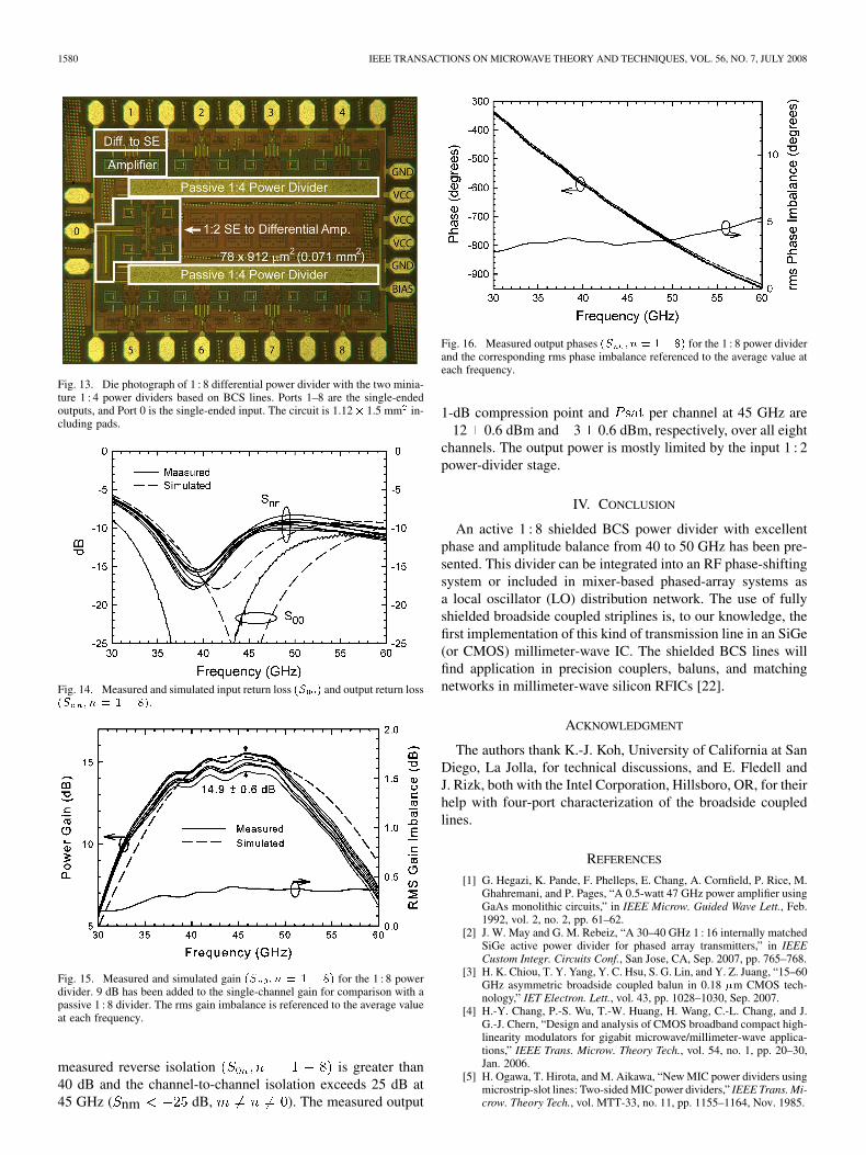
Fig. 13. Die photograph of 1 : 8 differential power divider with the two minia-ture 1 : 4 power dividers based on BCS lines. Ports 1–8 are the single-endedoutputs, and Port 0 is the single-ended input. The circuit is 1.12� 1.5 mm in-cluding pads.
Fig. 14. Measured and simulated input return loss (S ) and output return loss(S ; n = 1 � 8).
Fig. 15. Measured and simulated gain (S ; n = 1 � 8) for the 1 : 8 powerdivider. 9 dB has been added to the single-channel gain for comparison with apassive 1 : 8 divider. The rms gain imbalance is referenced to the average valueat each frequency.
measured reverse isolation is greater than40 dB and the channel-to-channel isolation exceeds 25 dB at45 GHz ( nm dB, ). The measured output
Fig. 16. Measured output phases (S ; n = 1� 8) for the 1 : 8 power dividerand the corresponding rms phase imbalance referenced to the average value ateach frequency.
1-dB compression point and per channel at 45 GHz are12 0.6 dBm and 3 0.6 dBm, respectively, over all eight
channels. The output power is mostly limited by the input 1 : 2power-divider stage.
IV. CONCLUSION
An active 1 : 8 shielded BCS power divider with excellentphase and amplitude balance from 40 to 50 GHz has been pre-sented. This divider can be integrated into an RF phase-shiftingsystem or included in mixer-based phased-array systems asa local oscillator (LO) distribution network. The use of fullyshielded broadside coupled striplines is, to our knowledge, thefirst implementation of this kind of transmission line in an SiGe(or CMOS) millimeter-wave IC. The shielded BCS lines willfind application in precision couplers, baluns, and matchingnetworks in millimeter-wave silicon RFICs [22].
ACKNOWLEDGMENT
The authors thank K.-J. Koh, University of California at SanDiego, La Jolla, for technical discussions, and E. Fledell andJ. Rizk, both with the Intel Corporation, Hillsboro, OR, for theirhelp with four-port characterization of the broadside coupledlines.
REFERENCES
[1] G. Hegazi, K. Pande, F. Phelleps, E. Chang, A. Cornfield, P. Rice, M.Ghahremani, and P. Pages, “A 0.5-watt 47 GHz power amplifier usingGaAs monolithic circuits,” in IEEE Microw. Guided Wave Lett., Feb.1992, vol. 2, no. 2, pp. 61–62.
[2] J. W. May and G. M. Rebeiz, “A 30–40 GHz 1 : 16 internally matchedSiGe active power divider for phased array transmitters,” in IEEECustom Integr. Circuits Conf., San Jose, CA, Sep. 2007, pp. 765–768.
[3] H. K. Chiou, T. Y. Yang, Y. C. Hsu, S. G. Lin, and Y. Z. Juang, “15–60GHz asymmetric broadside coupled balun in 0.18 �m CMOS tech-nology,” IET Electron. Lett., vol. 43, pp. 1028–1030, Sep. 2007.
[4] H.-Y. Chang, P.-S. Wu, T.-W. Huang, H. Wang, C.-L. Chang, and J.G.-J. Chern, “Design and analysis of CMOS broadband compact high-linearity modulators for gigabit microwave/millimeter-wave applica-tions,” IEEE Trans. Microw. Theory Tech., vol. 54, no. 1, pp. 20–30,Jan. 2006.
[5] H. Ogawa, T. Hirota, and M. Aikawa, “New MIC power dividers usingmicrostrip-slot lines: Two-sided MIC power dividers,” IEEE Trans. Mi-crow. Theory Tech., vol. MTT-33, no. 11, pp. 1155–1164, Nov. 1985.

MAY AND REBEIZ: 40–50-GHz SiGe 1 : 8 DIFFERENTIAL POWER DIVIDER USING SHIELDED BROADSIDE-COUPLED STRIPLINES 1581
[6] T. Tokumitsu, S. Hara, and M. Aikawa, “Very small ultra-wide-bandMMIC magic T and applications to combiners and dividers,” IEEETrans. Microw. Theory Tech., vol. 37, no. 12, pp. 1985–1990, Dec.1989.
[7] T. O. Dickson, M. LaCroix, S. Boret, D. Gloria, R. Beerkens, andS. Voinigescu, “30–100-GHz inductors and transformers for mil-limeter-wave (Bi)CMOS integrated circuits,” IEEE Trans. Microw.Theory Tech., vol. 53, no. 1, pp. 123–133, Jan. 2005.
[8] B. A. Floyd, S. K. Reynolds, U. R. Pfeiffer, T. Zwick, T. Beukema, andB. Gaucher, “SiGe bipolar transceiver circuits operating at 60 GHz,”IEEE J. Solid-State Circuits., vol. 40, no. 1, pp. 156–167, Jan. 2005.
[9] D. Goren et al., “On-chip interconnect-aware design and modelingmethodology based on high bandwidth transmission line devices,” inProc. Design Automat. Conf., Jun. 2003, pp. 724–727.
[10] S. B. Cohn, “Characteristic impedances of broadside-coupled transmis-sion lines,” IEEE Trans. Microw. Theory Tech., vol. MTT-8, no. 6, pp.633–637, Nov. 1960.
[11] F. Oberhettinger and W. Magnus, Applications of Elliptic Functions inPhysics and Technology. New York: Springer, 1949.
[12] S. B. Cohn, “Thickness corrections for capacitive obstacles and stripconductors,” IEEE Trans. Microw. Theory Tech., vol. MTT-8, no. 6,pp. 638–644, Nov. 1960.
[13] “Sonnet User’s Manual, Release 9.0,” Sonnet Softw. Inc., North Syra-cuse, NY, 2007.
[14] “Agilent ADS 2007 User’s Manual,” Agilent Technol., Santa Clara,CA, 2007.
[15] “Ansoft HFSS 10.1.3 User’s Manual,” Ansoft Corporation, Pittsburgh,PA, 2006.
[16] D. E. Bockelman and W. R. Eisenstadt, “Combined differential andcommon-mode scattering parameters: Theory and simulation,” IEEETrans. Microw. Theory Tech., vol. 43, no. 7, pp. 1530–1539, Jul. 1995.
[17] S. Baek, S. Ahn, J. Park, and J. Kim, “Accurate high frequencylossy model of differential signal line including mode-conversionand common-mode propagation,” in IEEE Int. Electromagn. Compat.Symp., Santa Clara, CA, Aug. 2004, pp. 562–566.
[18] Y. Eo and W. R. Eisenstadt, “High-speed VLSI interconnect modelingbased onS-parameter measurements,” IEEE Trans. Compon., Hybrids,Manuf. Technol., vol. 16, no. 5, pp. 555–562, Aug. 1993.
[19] “Jazz Semiconductor process details,” Jazz Semiconduct. Inc., New-port Beach, CA, 2007. [Online]. Available: http://www.jazzsemi.com
[20] M. Ferndahl et al., “CMOS MMICs for Microwave and MillimeterWave Applications,” in 15th Int. Microw., Radar, Wireless Commun.Conf., Warsaw, Poland, May 2004, pp. 237–248.
[21] V. Teppati and A. Ferrero, “On-wafer calibration algorithm for par-tially leaky multiport vector network analyzers,” IEEE Trans. Microw.Theory Tech., vol. 53, no. 11, pp. 3665–3671, Nov. 2005.
[22] K.-J. Koh, J. W. May, and G. M. Rebeiz, “Q-band (40–45 GHz) 16-ele-ment phased-array transmitter in 0.18-�m SiGe BiCMOS technology,”presented at the IEEE RFIC Symp., Jun. 2008.
Jason W. May (S’04) received the B.S. degreein electrical engineering from The University ofMichigan at Ann Arbor, in 2004, the M.S. degreein electrical engineering from the University ofCalifornia at San Diego, La Jolla, in 2007, andis currently working toward the Ph.D. degree inelectrical engineering at the University of Californiaat San Diego.
He was with Q-DOT Inc. (now the Hittite Mi-crowave Corporation), Colorado Springs, CO, asan Intern in 2003 and 2004, and as an Electrical
Engineer in 2005. His research interests include ICs for millimeter-wavephased-array applications.
Gabriel M. Rebeiz (S’86–M’88–SM’93–F’97) iscurrently a Professor of electrical engineering withthe University of California at San Diego (UCSD), LaJolla. He is the Director of the UCSD/North EasternUniversity (NEU) Defense Advanced ResearchProjects Agency (DARPA) Science and Technology(S&T) Center on RF MEMS. His research concernsplanar millimeter-wave and terahertz antennas andimaging arrays, RF MEMS, and millimeter-wave RFRFICs. He authored RF MEMS: Theory, Design andTechnology (Wiley, 2003).
Prof. Rebeiz is a National Science Foundation (NSF) Presidential Young In-vestigator. He was the recipient of a URSI Koga Gold Medal. He was a 2003IEEE Microwave Theory and Techniques Society (IEEE MTT-S) DistinguishedYoung Engineer. He was the recipient of the IEEE MTT–S 2000 MicrowavePrize and the 1998 Amoco Teaching Award given to the best undergraduateteacher at The University of Michigan at Ann Arbor.