3OHDVH QRWHG - ntut.edu.tdkao/chap01.pdf · 9/6, 'hvljq &kdswhu 2shq ,vvxhv 0lfurvfrslf lvvxhv...
120
VLSI Design : Chapter 5-1 1 Introduction to VLSI Design Textbook: Modern VLSI Design IP-Based Design, Third edition, Prentice Hall, by: Wayne Wolf
Transcript of 3OHDVH QRWHG - ntut.edu.tdkao/chap01.pdf · 9/6, 'hvljq &kdswhu 2shq ,vvxhv 0lfurvfrslf lvvxhv...

VLSI Design : Chapter 5-1 1
Introduction to VLSI Design
Textbook:
Modern VLSI Design
IP-Based Design,
Third edition, Prentice Hall,
by: Wayne Wolf
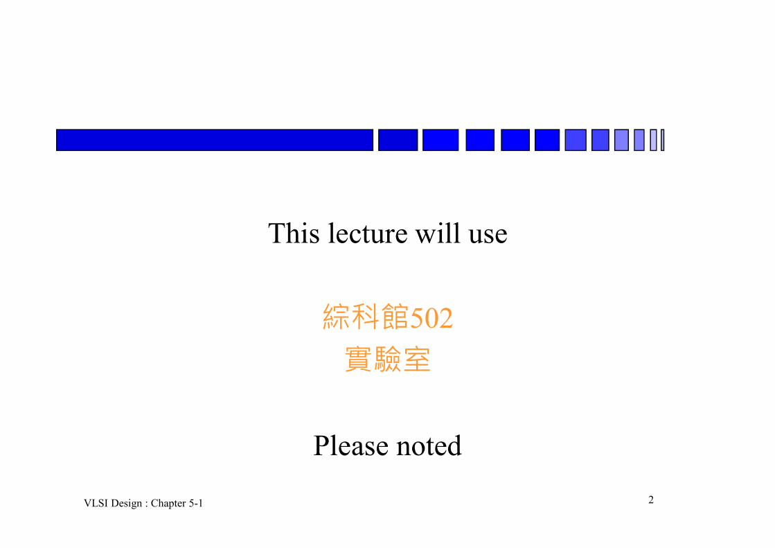
VLSI Design : Chapter 5-1 2
This lecture will use
綜科館502
實驗室
Please noted

VLSI Design : Chapter 5-1 3
References
ULSI 製程技術 (新文京開發出版)
by: 劉博文
Digital Integrated Circuits
A Design Perspective
By: Jan M. Rabaey, Anantha Chandrakasan, and Borivoje Nikolić

VLSI Design : Chapter 5-1 4
Instructor
高得畬 Kao, De-YuE-mail: [email protected]
Class Notes:http://www.cc.ntut.edu.tw/~dkao/
If possible, please down load the material right before the class…… :-p

VLSI Design : Chapter 5-1 5
Grading Policy
Two quizzes 30% (15% for each)
Midterm 35%
Final 35%VLSI

VLSI Design : Chapter 5-1 6
Schedule (1)
01. 03/01/18 Chapter 1 Introduction (Moore’s rule)
02. 03/08/18 Chapter 1 Introduction (Cost and TW)
03. 03/15/18 Chapter 2 (Mask)
04. 03/22/18 Chapter 2 (Processing)
05. 03/29/18 Quiz 1, Chapter 2 (Transistors)
06. 04/05/18 清明節
07. 04/12/18 Chapter 2 (Cross-section , latch up)
VLSI Design : Chapter 5-1 7
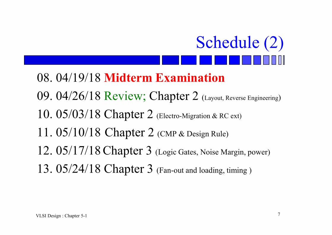
Schedule (2)
08. 04/19/18 Midterm Examination
09. 04/26/18 Review; Chapter 2 (Layout, Reverse Engineering)
10. 05/03/18 Chapter 2 (Electro-Migration & RC ext)
11. 05/10/18 Chapter 2 (CMP & Design Rule)
12. 05/17/18 Chapter 3 (Logic Gates, Noise Margin, power)
13. 05/24/18 Chapter 3 (Fan-out and loading, timing )
VLSI Design : Chapter 5-1 8
Schedule (3)
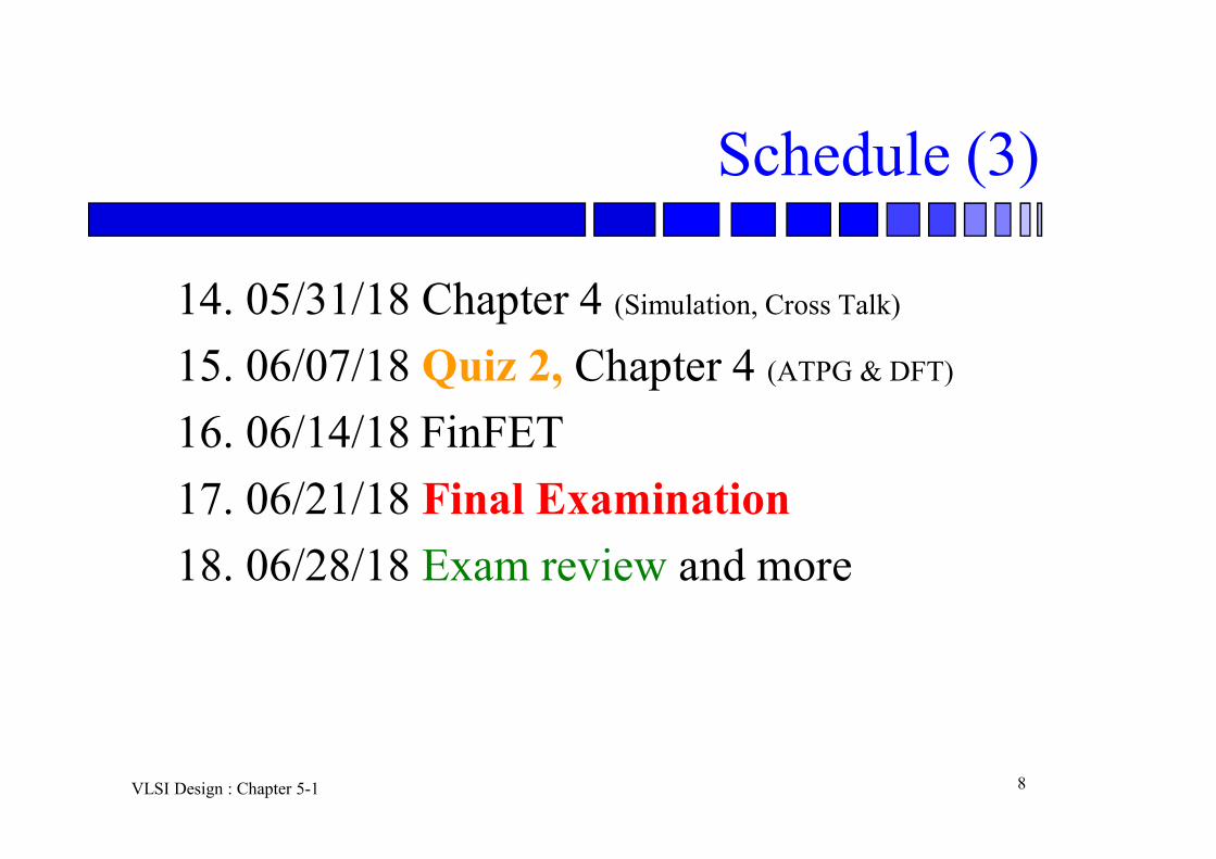
14. 05/31/18 Chapter 4 (Simulation, Cross Talk)
15. 06/07/18 Quiz 2, Chapter 4 (ATPG & DFT)
16. 06/14/18 FinFET
17. 06/21/18 Final Examination
18. 06/28/18 Exam review and more

VLSI Design : Chapter 5-1 9
Preview for Next Semester
Add-on Packaging
Chapter 5 Sequential Machines (Memories)
Chapter 6 CPU / ALU, Data-path
Chapter 7 CAD
Chapter 8 Architecture
Chapter 9 Examples
Add-on What’s next?
VLSI Design : Chapter 5-1 10
Time for the class
18:40

VLSI Design : Chapter 5-1 11
Questions ??.

VLSI Design : Chapter 5-1 12
Chapter One
Overview
VLSI?
Moore’s Law
The Difficulties in VLSI Design
Cost of the VLSI Design
Taiwan VLSI Related Industry
VLSI Design : Chapter 5-1 13
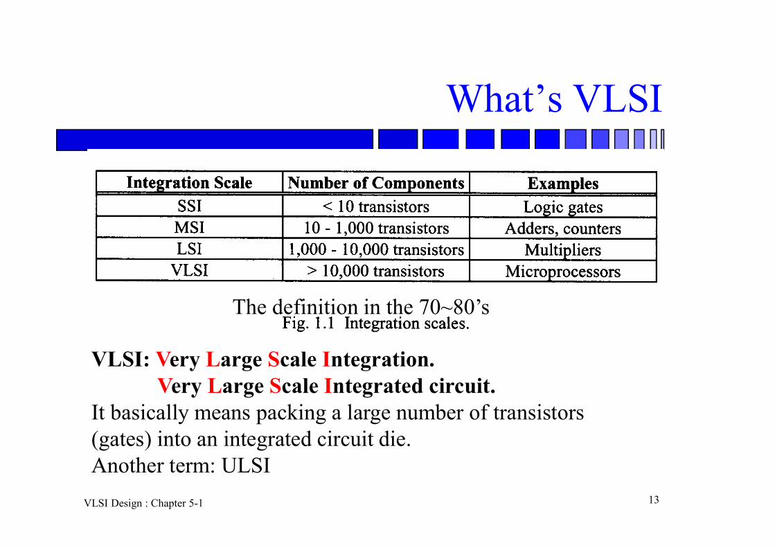
What’s VLSI
The definition in the 70~80’s
VLSI: Very Large Scale Integration. Very Large Scale Integrated circuit.
It basically means packing a large number of transistors (gates) into an integrated circuit die.Another term: ULSI

VLSI Design : Chapter 5-1 14
電子元件
二極體
電容
電晶體
電阻

VLSI Design : Chapter 5-1 15
電阻
二極體
電容
電晶體
IC =
+
+
+

VLSI Design : Chapter 5-1 16

VLSI Design : Chapter 5-1 17
Where have you seen ICs?

VLSI Design : Chapter 5-1 18
Where have you seen ICs?
VLSI Design : Chapter 5-1 19
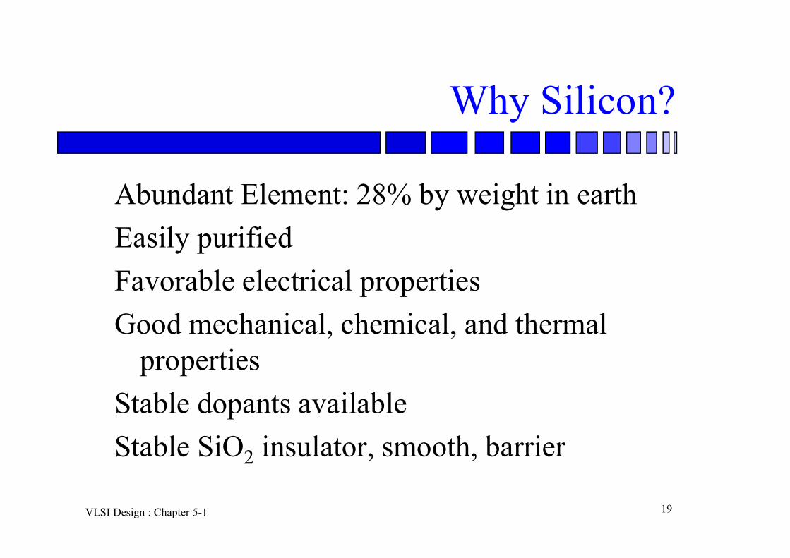
Why Silicon?
Abundant Element: 28% by weight in earth
Easily purified
Favorable electrical properties
Good mechanical, chemical, and thermal properties
Stable dopants available
Stable SiO2 insulator, smooth, barrier
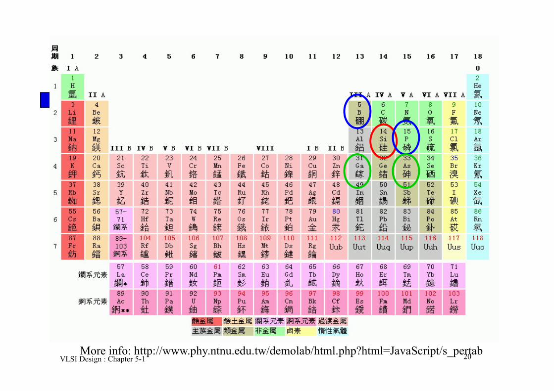
VLSI Design : Chapter 5-1 20More info: http://www.phy.ntnu.edu.tw/demolab/html.php?html=JavaScript/s_pertab

VLSI Design : Chapter 5-1 21
Why VLSI?
Integration improves the design:lower parasitics, higher speed
lower power
physically smaller
lower cost
Integration reduces manufacturing cost-(almost) no manual assembly.
VLSI Design : Chapter 5-1 22
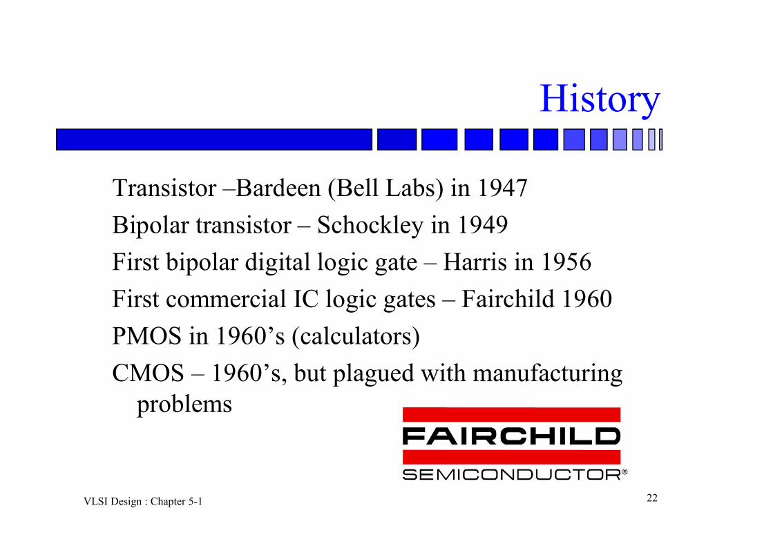
History
Transistor –Bardeen (Bell Labs) in 1947
Bipolar transistor – Schockley in 1949
First bipolar digital logic gate – Harris in 1956
First commercial IC logic gates – Fairchild 1960
PMOS in 1960’s (calculators)
CMOS – 1960’s, but plagued with manufacturing problems

VLSI Design : Chapter 5-1 23
History
NMOS in 1970’s (4004, 8080) – for speed
CMOS in 1980’s – preferred technology because of power benefits
Now, Copper (Low K), Hi-K, SOI, HiV…
Fin-FET
From left to right: Gordon Moore, C. Sheldon Roberts, Eugene Kleiner, Robert Noyce, Victor Grinich, Julius Blank, Jean Hoerni and Jay Last. (1960) traitorous eight
VLSI Design : Chapter 5-1 24
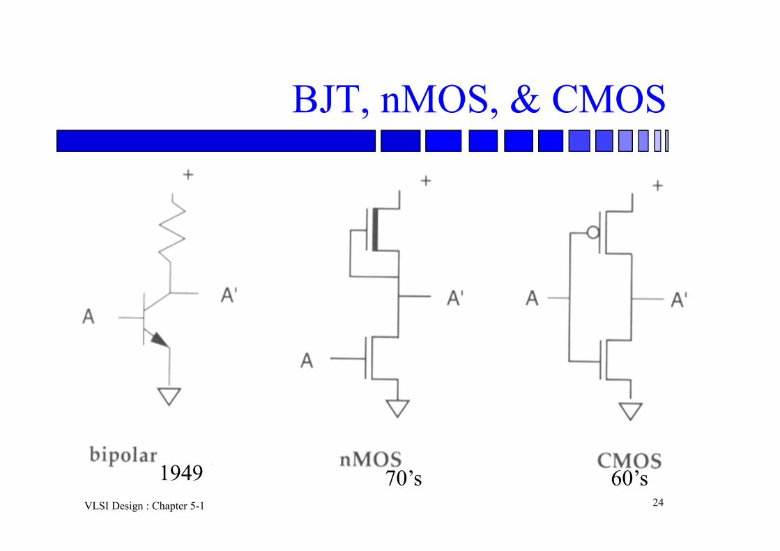
BJT, nMOS, & CMOS
1949 70’s 60’s
VLSI Design : Chapter 5-1 25
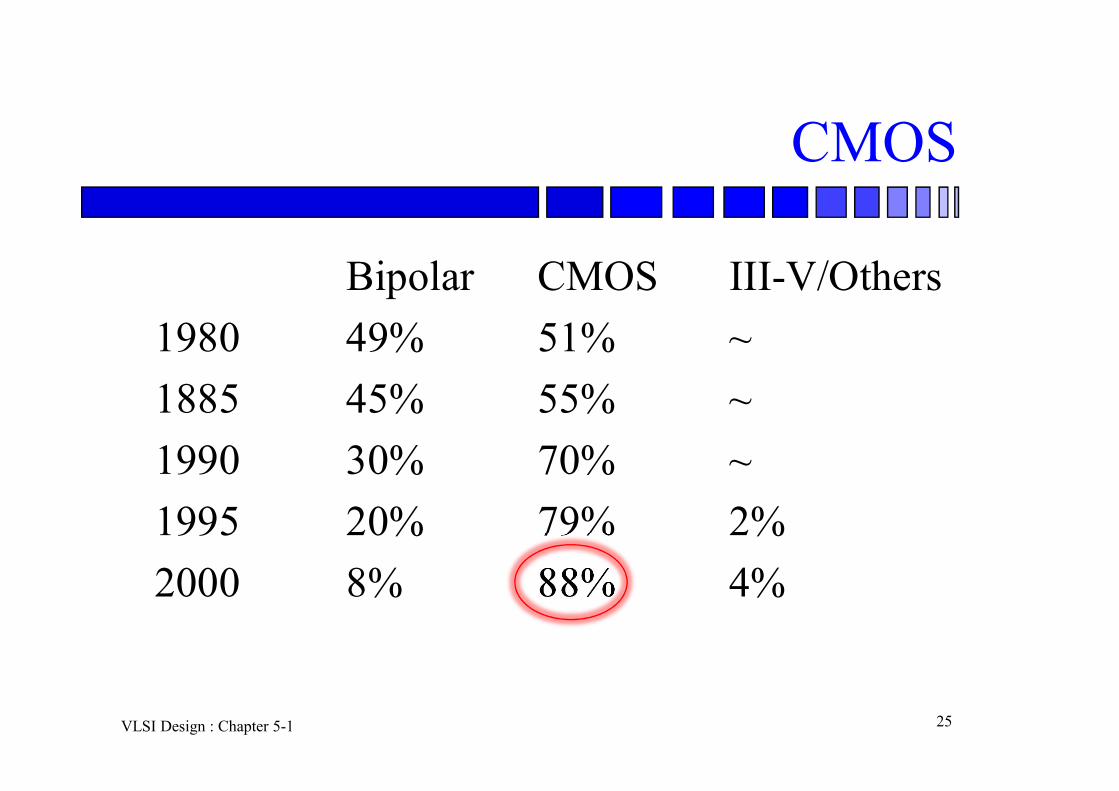
CMOS
Bipolar CMOS III-V/Others
1980 49% 51% ~
1885 45% 55% ~
1990 30% 70% ~
1995 20% 79% 2%
2000 8% 88% 4%

VLSI Design : Chapter 5-1 26
Applications
Microprocessors:personal computersMicrocontrollersSpecial-purpose processors
Memories (DRAM/SRAM).Drivers (video displayers, motors, audio speakers,
lights…. )Hi-freq. PHY (TX/RX)SOC, mixed mode, MEMS, Bio-Chips……

VLSI Design : Chapter 5-1 27
MilitaryCar
Industrial
IC 廣泛應用於各式各樣電子產品
Computer
CommunicationConsumer
Medicine
VLSI Design : Chapter 5-1 28
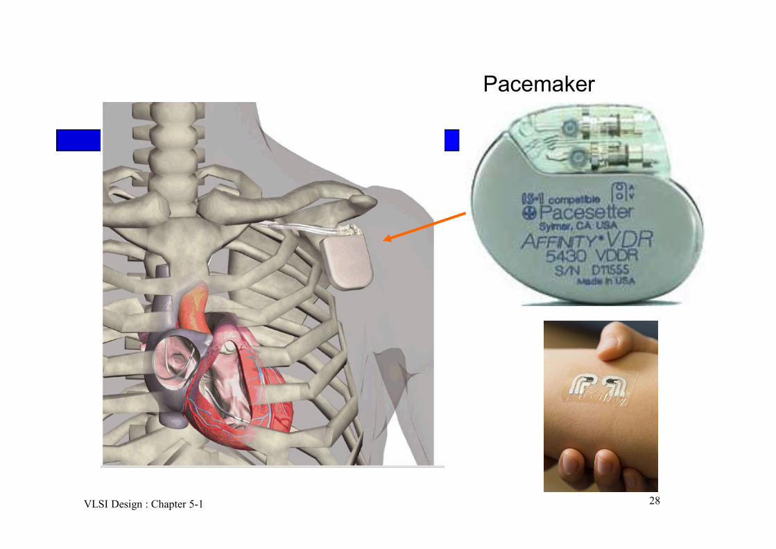
Pacemaker

VLSI Design : Chapter 5-1 29
沒有發明半導體的話
真空管2.4m
電腦的體積會 ~ 無線手機的大小將 ~
ATLAS (2700個真空管)
VLSI Design : Chapter 5-1 30
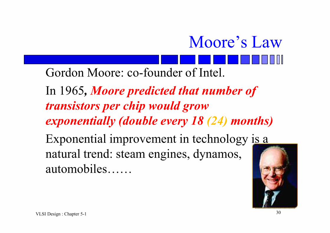
Moore’s Law
Gordon Moore: co-founder of Intel.
In 1965, Moore predicted that number of transistors per chip would grow exponentially (double every 18 (24) months)
Exponential improvement in technology is a natural trend: steam engines, dynamos, automobiles……

VLSI Design : Chapter 5-1 31
Moore’s Law
Sou
rce:
Wik
iped
ia
VLSI Design : Chapter 5-1 32
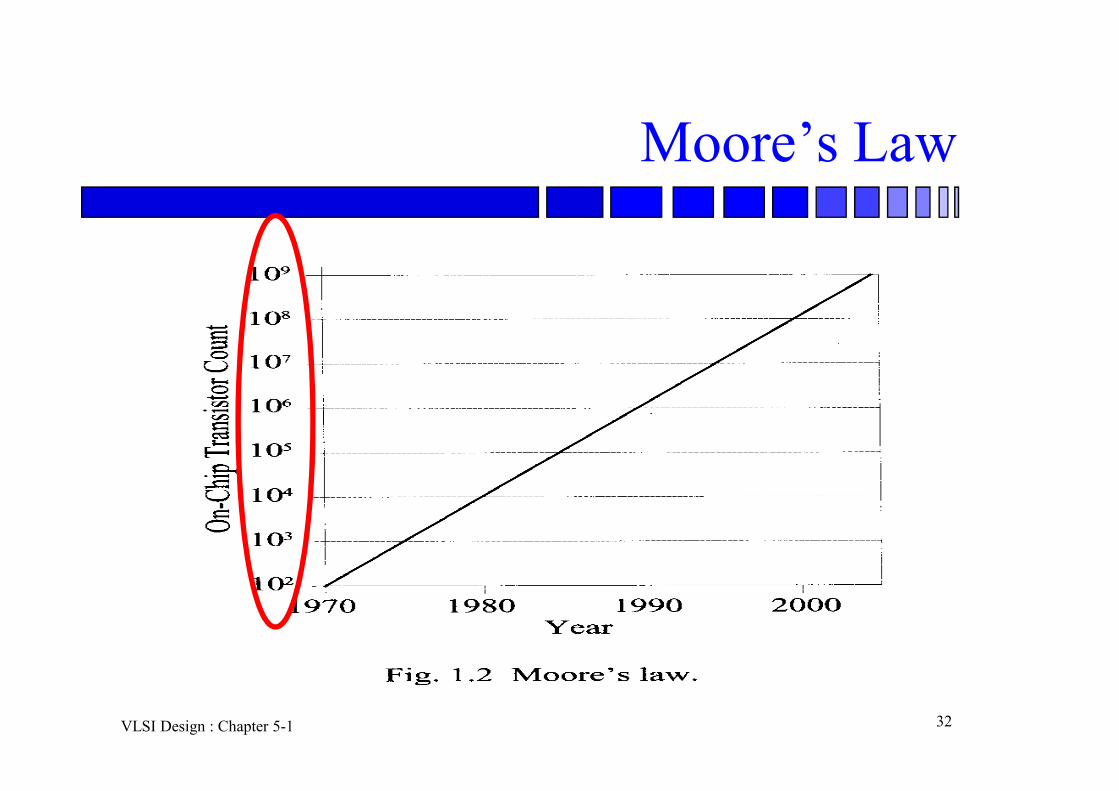
Moore’s Law
VLSI Design : Chapter 5-1 33
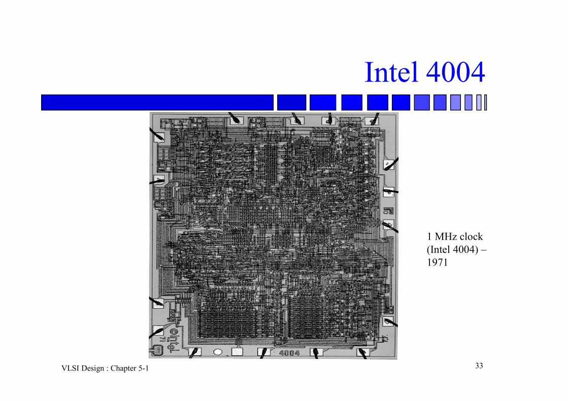
Intel 4004
1 MHz clock (Intel 4004) –1971
VLSI Design : Chapter 5-1 34
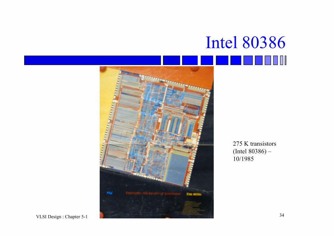
Intel 80386
275 K transistors (Intel 80386) –10/1985
VLSI Design : Chapter 5-1 35
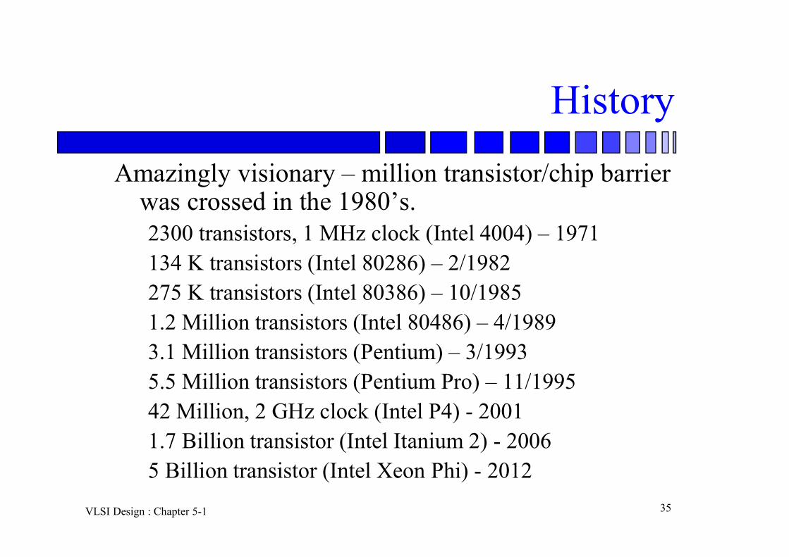
History
Amazingly visionary – million transistor/chip barrier was crossed in the 1980’s.2300 transistors, 1 MHz clock (Intel 4004) – 1971134 K transistors (Intel 80286) – 2/1982275 K transistors (Intel 80386) – 10/19851.2 Million transistors (Intel 80486) – 4/19893.1 Million transistors (Pentium) – 3/19935.5 Million transistors (Pentium Pro) – 11/199542 Million, 2 GHz clock (Intel P4) - 20011.7 Billion transistor (Intel Itanium 2) - 20065 Billion transistor (Intel Xeon Phi) - 2012

VLSI Design : Chapter 5-1 36
Intel Pentium IV
42 Million, 2 GHz clock (Intel P4) -2001
VLSI Design : Chapter 5-1 37
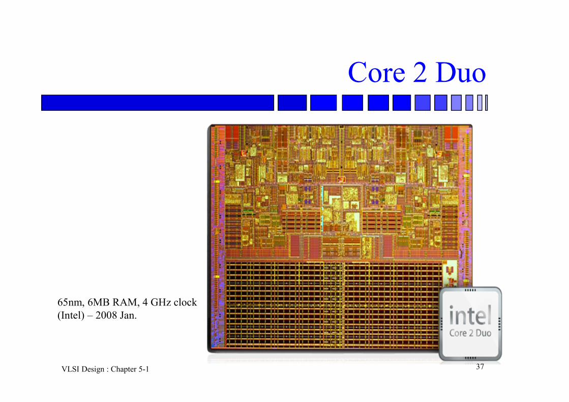
Core 2 Duo
65nm, 6MB RAM, 4 GHz clock (Intel) – 2008 Jan.

VLSI Design : Chapter 5-1 38
Apple A6
32nm,, 1.3 GHz clock(Apple) –2012 Sep. Used in iPhone5
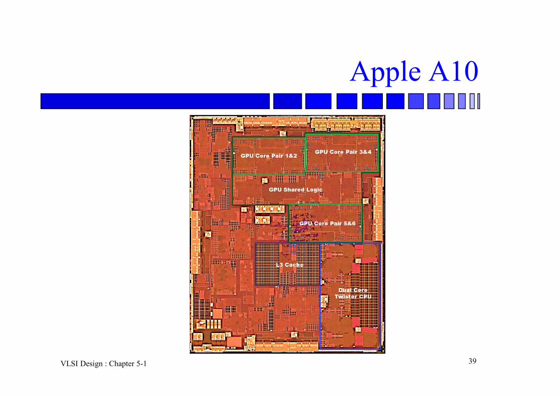
VLSI Design : Chapter 5-1 39
Apple A10

VLSI Design : Chapter 5-1 40
Graphical illustration of Moore’s law
1981 1984 1987 1990 1993 1996 1999 2002
Leading edgechip in 1981
10,000transistors
Leading edgechip in 2002
150,000,000transistors
Something that doubles frequently grows more quickly than most people realize!A 2002 chip can hold about 15,000 1981 chips inside
itself

VLSI Design : Chapter 5-1 41
Progression
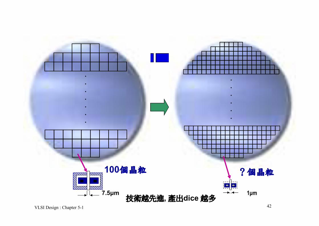
VLSI Design : Chapter 5-1 42
100個晶粒 ?個晶粒
.
.
.
.
.
.
.
.
.
.
.
.
.
7.5μm 1μm技術越先進, 產出dice 越多
VLSI Design : Chapter 5-1 43
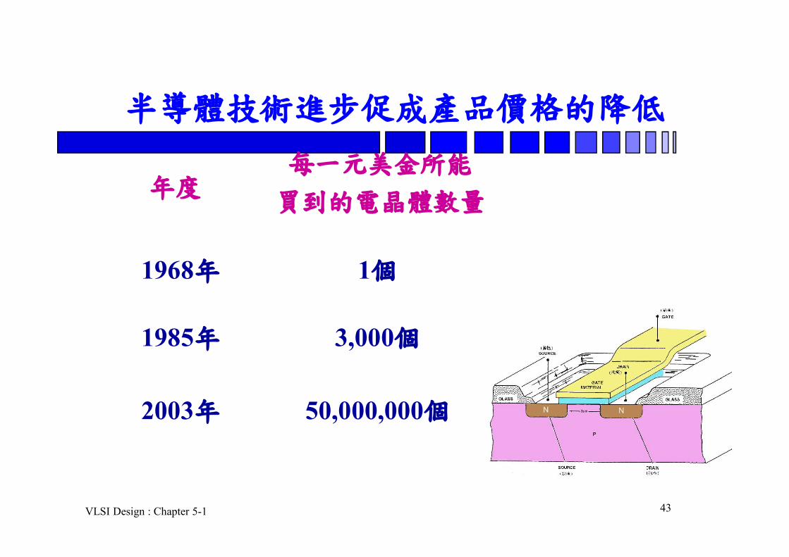
半導體技術進步促成產品價格的降低
年度每一元美金所能
買到的電晶體數量
1968年 1個
1985年 3,000個
2003年 50,000,000個
VLSI Design : Chapter 5-1 44
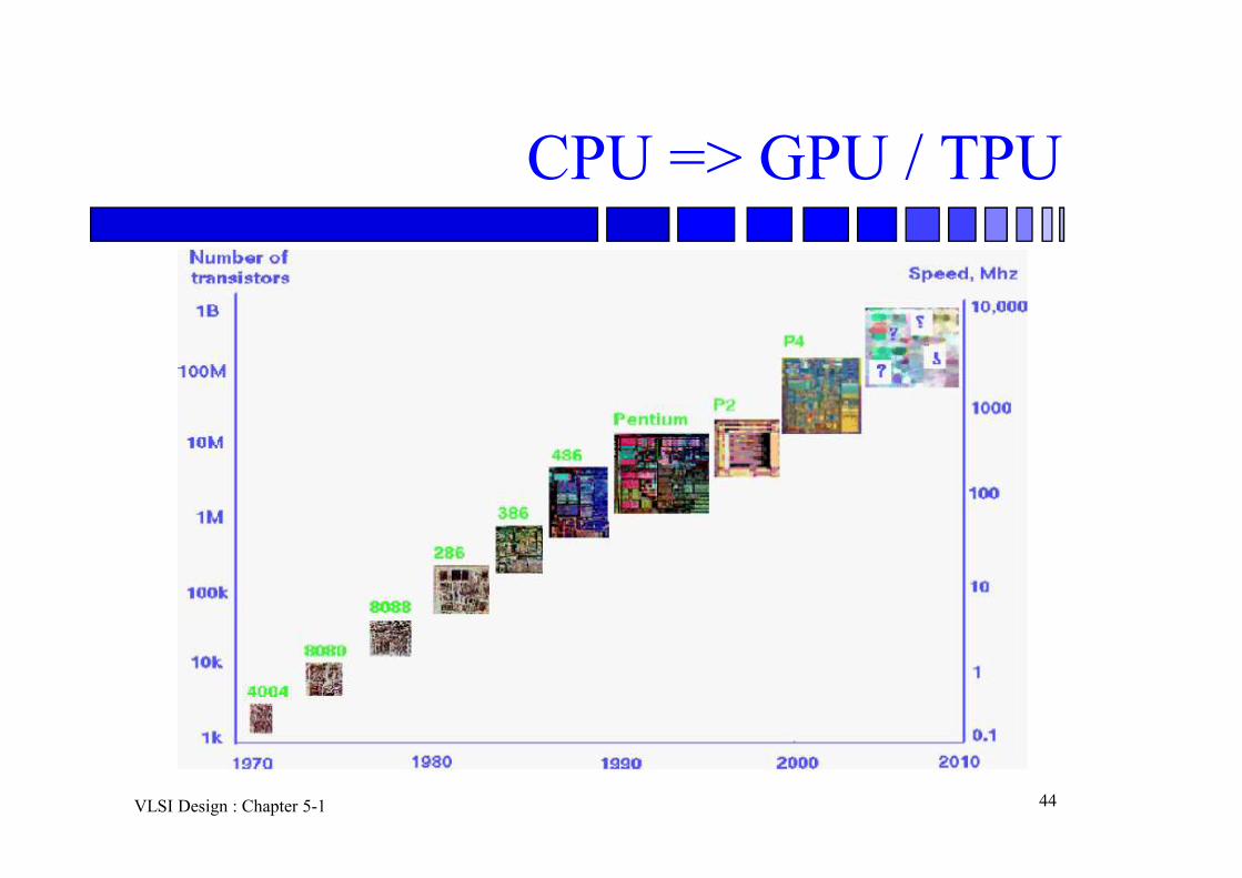
CPU => GPU / TPU
VLSI Design : Chapter 5-1 45
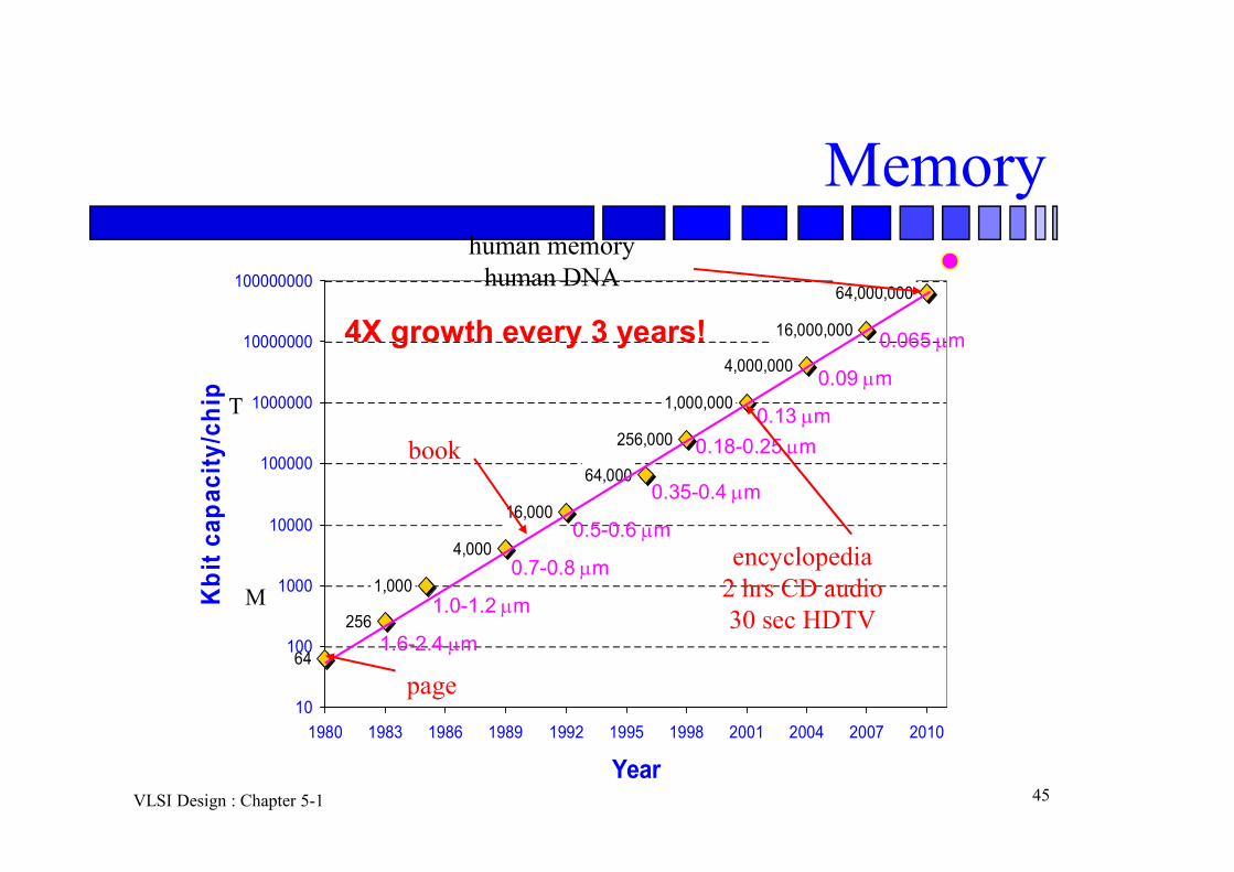
Memory
64
256
1,000
4,000
16,000
64,000
256,000
1,000,000
4,000,000
16,000,000
64,000,000
10
100
1000
10000
100000
1000000
10000000
100000000
1980 1983 1986 1989 1992 1995 1998 2001 2004 2007 2010
Year
Kb
it c
apac
ity/
chip
1.6-2.4 m
1.0-1.2 m
0.7-0.8 m
0.5-0.6 m
0.35-0.4 m
0.18-0.25 m
0.13 m
0.09 m
0.065 m
human memoryhuman DNA
encyclopedia2 hrs CD audio30 sec HDTV
book
page
4X growth every 3 years!
T
M
VLSI Design : Chapter 5-1 46
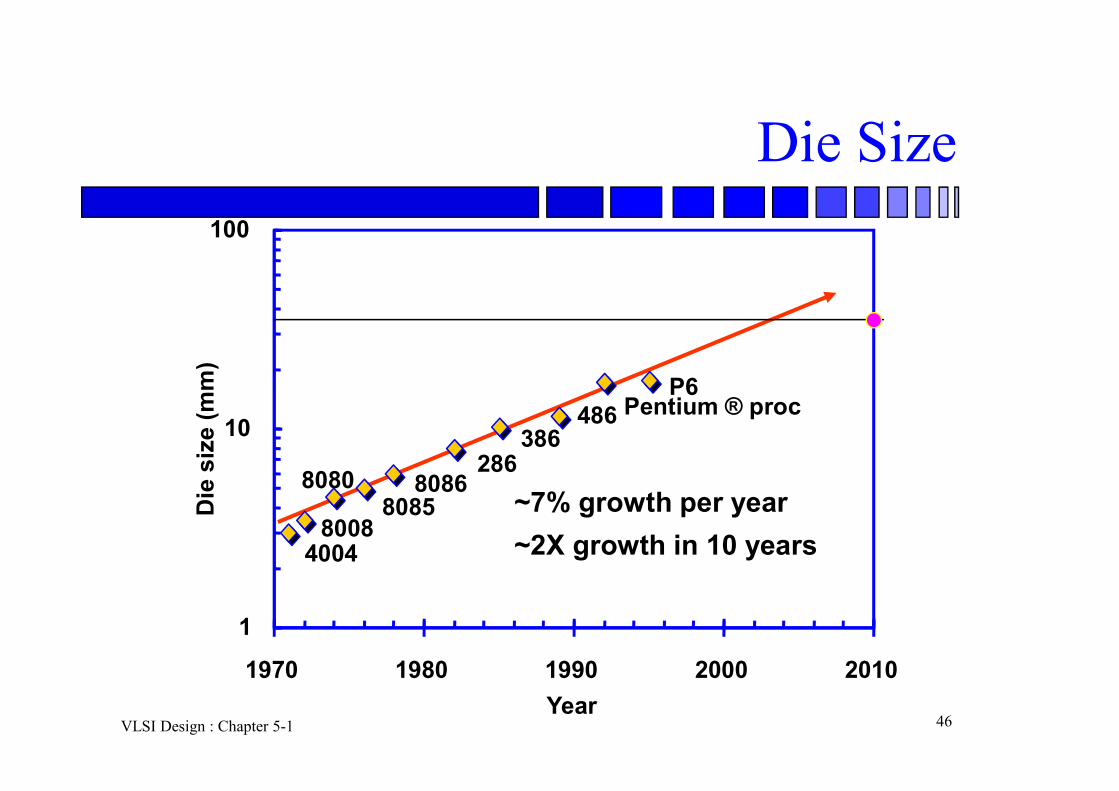
Die Size
40048008
80808085
8086286
386486 Pentium ® proc
P6
1
10
100
1970 1980 1990 2000 2010
Year
Die
siz
e (m
m)
~7% growth per year
~2X growth in 10 years
VLSI Design : Chapter 5-1 47
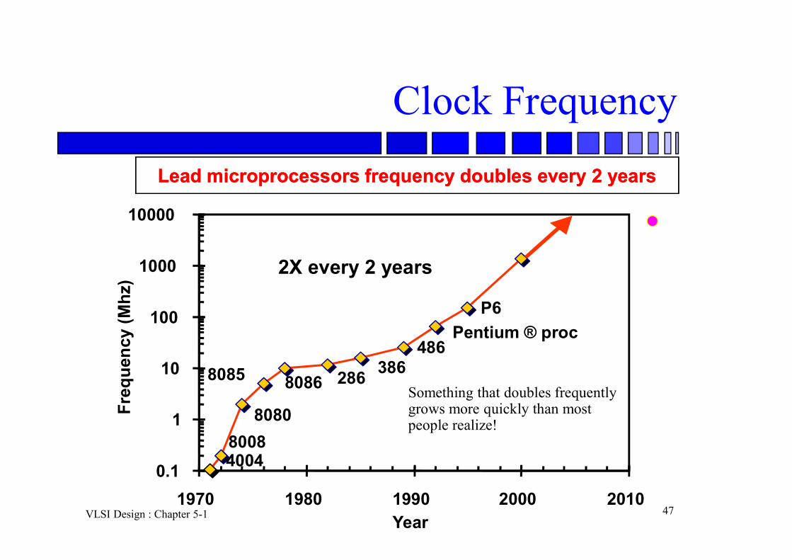
Clock Frequency
Lead microprocessors frequency doubles every 2 yearsLead microprocessors frequency doubles every 2 years
P6
Pentium ® proc486
38628680868085
8080
80084004
0.1
1
10
100
1000
10000
1970 1980 1990 2000 2010Year
Fre
qu
ency
(M
hz)
2X every 2 years
Something that doubles frequently grows more quickly than most people realize!

VLSI Design : Chapter 5-1 48
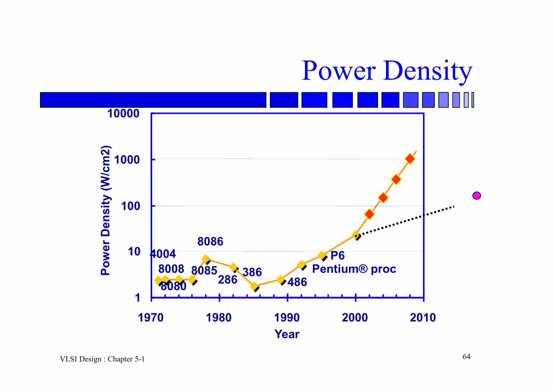
Power
Lead Microprocessors power continues to increase
P6Pentium ® proc
486
3862868086
80858080
80084004
0.1
1
10
100
1971 1974 1978 1985 1992 2000Year
Po
we
r (W
atts
)
Courtesy, Intel
Power delivery and dissipation will be prohibitive
VLSI Design : Chapter 5-1 49
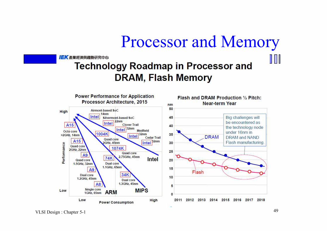
Processor and Memory
VLSI Design : Chapter 5-1 50
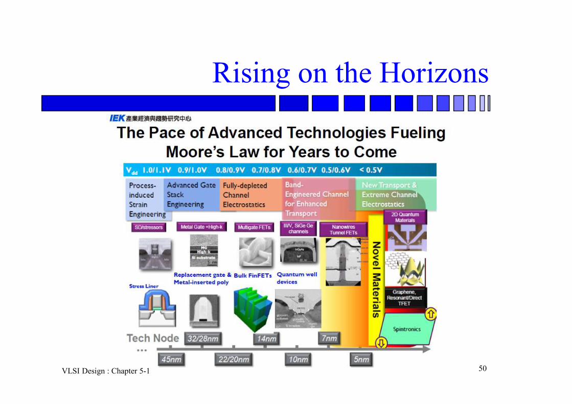
Rising on the Horizons

VLSI Design : Chapter 5-1 51
More Moore’s
VLSI Design : Chapter 5-1 52
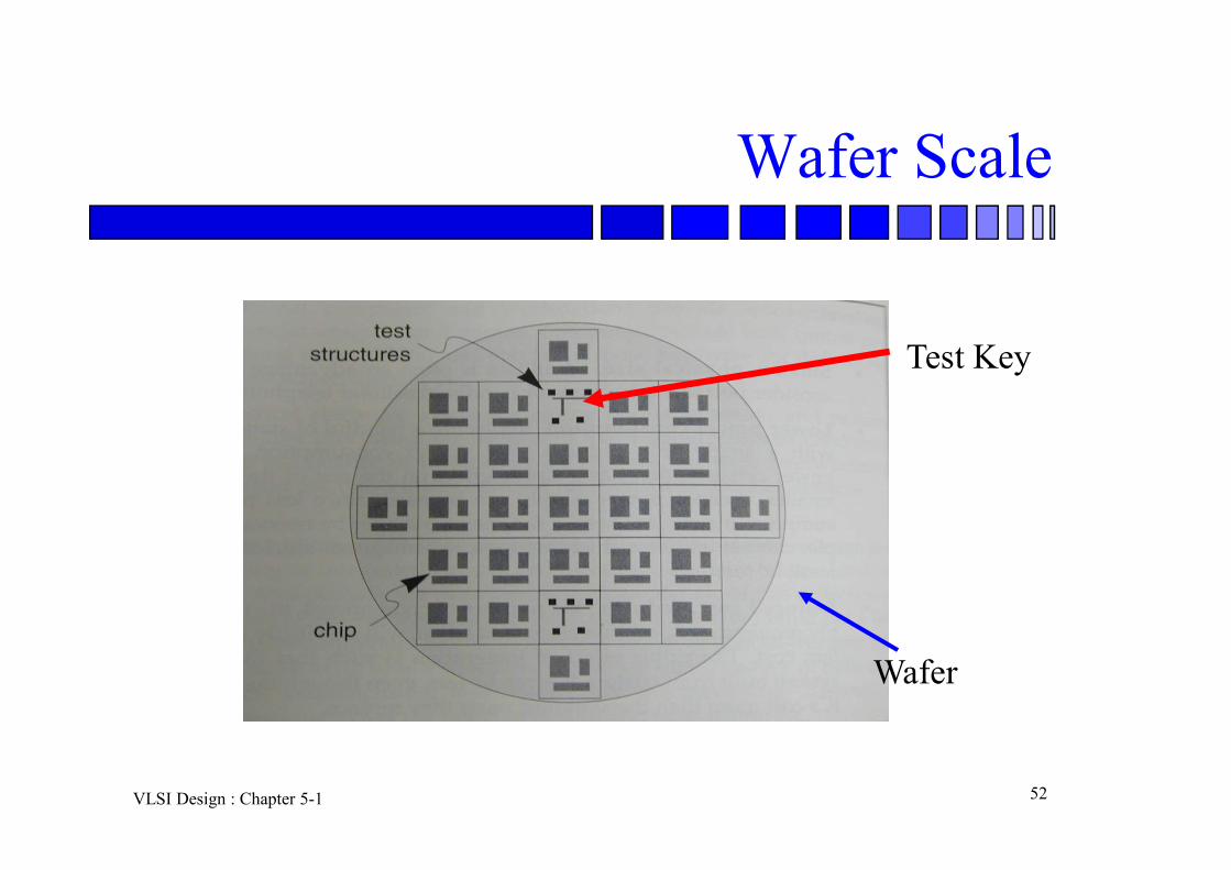
Wafer Scale
Test Key
Wafer

VLSI Design : Chapter 5-1 53
First 3.2-Million Gate Virtex-EA FPGA
Courtesy of Xilinx, Inc.
XCV3200EA manufactured by UMC’s 0.15um process
• Fab 8” 0.15um CMOS
• 1.8V Core, 3.3V I/O
• 1P/6LM, Dual-gate Oxide
• 225 Million Transistors
• 3. 2M Gate-Count FPGA
• Top 2 Cu Layers to be
Offered
VLSI Design : Chapter 5-1 54
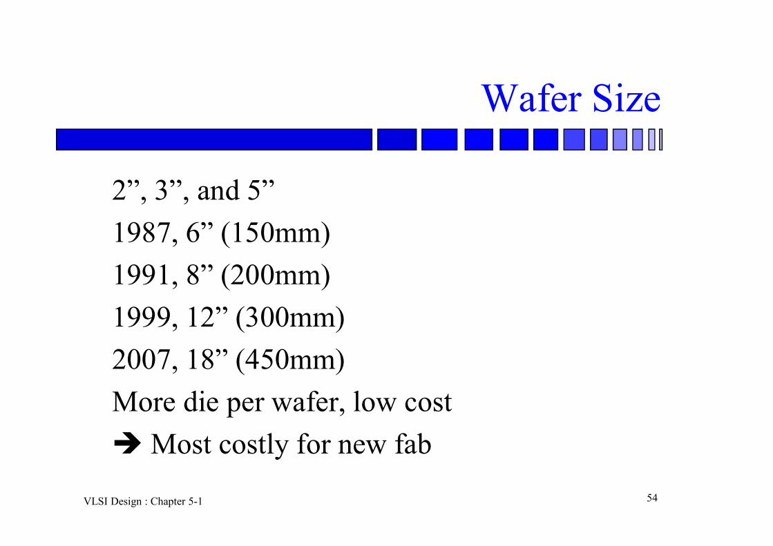
Wafer Size
2”, 3”, and 5”
1987, 6” (150mm)
1991, 8” (200mm)
1999, 12” (300mm)
2007, 18” (450mm)
More die per wafer, low cost
Most costly for new fab

VLSI Design : Chapter 5-1 55
Bigger Wafer Size - Higher productivity
12” wafer8” wafer
1 2
3 4
Unit Productivity Comparison1
2.25倍
2
6
7
543
9
1211
8 10
Wafer Size : 1 : 2.25 Gross Die : 1 : 3
晶圓越大, 產出dice 越多
VLSI Design : Chapter 5-1 56
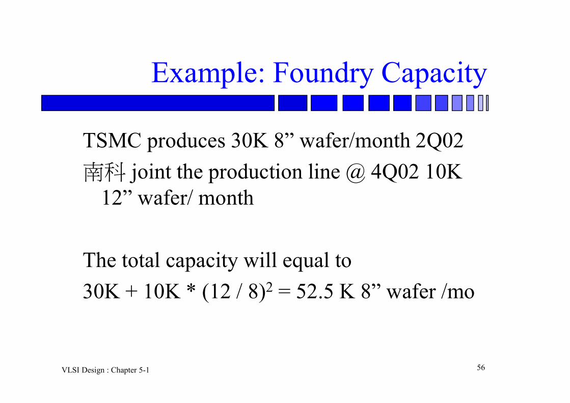
Example: Foundry Capacity
TSMC produces 30K 8” wafer/month 2Q02
南科 joint the production line @ 4Q02 10K 12” wafer/ month
The total capacity will equal to
30K + 10K * (12 / 8)2 = 52.5 K 8” wafer /mo

VLSI Design : Chapter 5-1 57
Tech Roadmap
18617717116013010690Max P power [W]
1.4
1.2
6-7
1.5-1.8
180
1999
1.7
1.6-1.4
6-7
1.5-1.8
162
2000
14.9-3.6
11-37.1-2.53.5-22.1-1.6Max freq [GHz],
Local-Global
2.52.32.12.42.0Bat. power [W]
109-10987Wiring levels
0.3-0.60.5-0.60.6-0.90.9-1.21.2-1.5Supply [V]
30456590130Technology node
[nm]
20132010200720042001Year of Introduction
Node: 2012/28nm; 2014/20nm; 2017/14nm running

VLSI Design : Chapter 5-1 58
A Real Case (UMC)

VLSI Design : Chapter 5-1 59
We will have all our lectures in
綜科館502實驗室
Please noted

VLSI Design : Chapter 5-1 60
Schedule (1)
01. 03/01/18 Chapter 1 Introduction (Moore’s rule)
02. 03/08/18 Chapter 1 Introduction (Cost and TW)
03. 03/15/18 Chapter 2 (Mask)
04. 03/22/18 Chapter 2 (Processing)
05. 03/29/18 Quiz 1, Chapter 2 (Transistors)
06. 04/05/18 清明節
07. 04/12/18 Chapter 2 (Cross-section , latch up)

VLSI Design : Chapter 5-1 61
Moore’s Law
Gordon Moore: co-founder of Intel.
In 1965, Moore predicted that number of transistors per chip would grow exponentially (double every 18 (24) months).
Exponential improvement in technology is a natural trend: steam engines, dynamos, automobiles……

VLSI Design : Chapter 5-1 62
Moore’s Law

VLSI Design : Chapter 5-1 63
182535
5070100130
180250350
500800
1 TB
(2023)
1
10
100
1000
10000
1989 1990 1993 1996 1999 2002 2005 2008 2011 2014 2017 2020 2023 2026
1.E+ 05
1.E+ 06
1.E+ 07
1.E+ 08
1.E+ 09
1.E+ 10
1.E+ 11
1.E+ 12
1.E+ 13
1.E+ 14
1.E+ 15
DRAM1.4 Times/Year
64GB(2015)
Neuron Number in Brain
Increasing Technology difficulty
Tran
sistor N
um
ber p
er chip
year
1015
1014
1013
1012
1011
1010
109
108
107
106
105
Gat
e L
en
gth
(n
m) 1TB
(2023)
Technology Scaling
90
14
VLSI Design : Chapter 5-1 64
Power Density
40048008
80808085
8086
286386
486Pentium® proc
P6
1
10
100
1000
10000
1970 1980 1990 2000 2010
Year
Po
we
r D
ensi
ty (
W/c
m2)
VLSI Design : Chapter 5-1 65
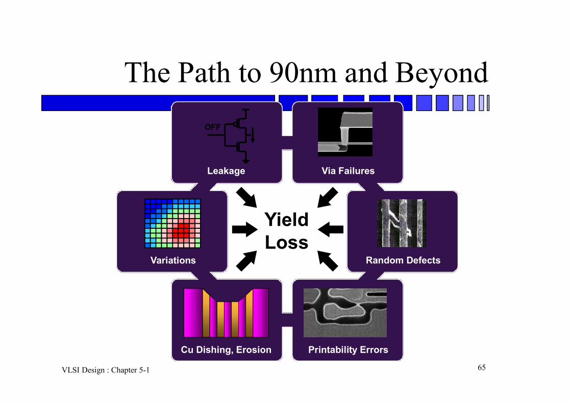
The Path to 90nm and Beyond
Random Defects
Via Failures
Cu Dishing, Erosion Printability Errors
Variations
Leakage
Yield Loss
OFF
VLSI Design : Chapter 5-1 66
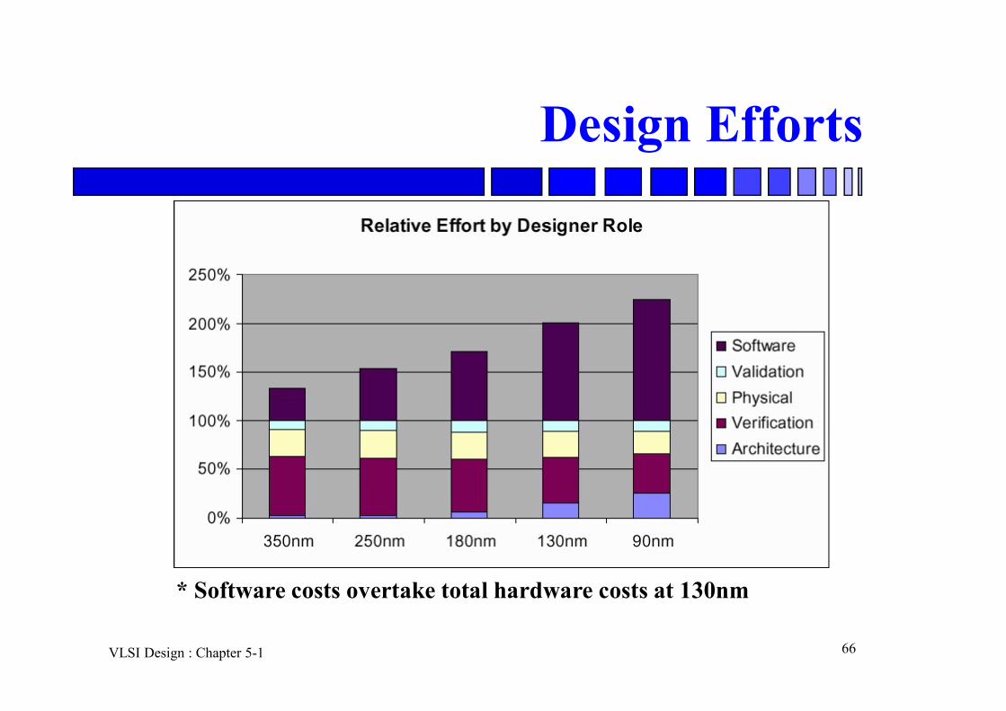
Design Efforts
* Software costs overtake total hardware costs at 130nm

VLSI Design : Chapter 5-1 67
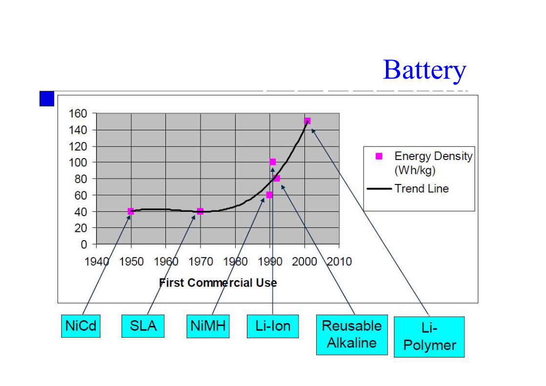
Energy Storage
Material KWH/kgGasoline 14Lead-Acid 0.04Li polymer 0.15
VLSI Design : Chapter 5-1 68
Battery

VLSI Design : Chapter 5-1 69
Productivity
200
3
198
1
198
3
198
5
198
7
198
9
199
1
199
3
199
5
199
7
199
9
200
1
200
5
200
7
200
9
Logic Tr./Chip
Tr./Staff Month.
xxx
xxx
x
21%/Yr. compoundProductivity growth rate
x
58%/Yr. compoundedComplexity growth rate
10,000
1,000
100
10
1
0.1
0.01
0.001
Lo
gic
Tra
ns
isto
r p
er C
hip
(M)
0.01
0.1
1
10
100
1,000
10,000
100,000
Pro
du
cti
vity
(K)
Tran
s./S
taff
-M
o.
Co
mp
lexi
ty
VLSI Design : Chapter 5-1 70
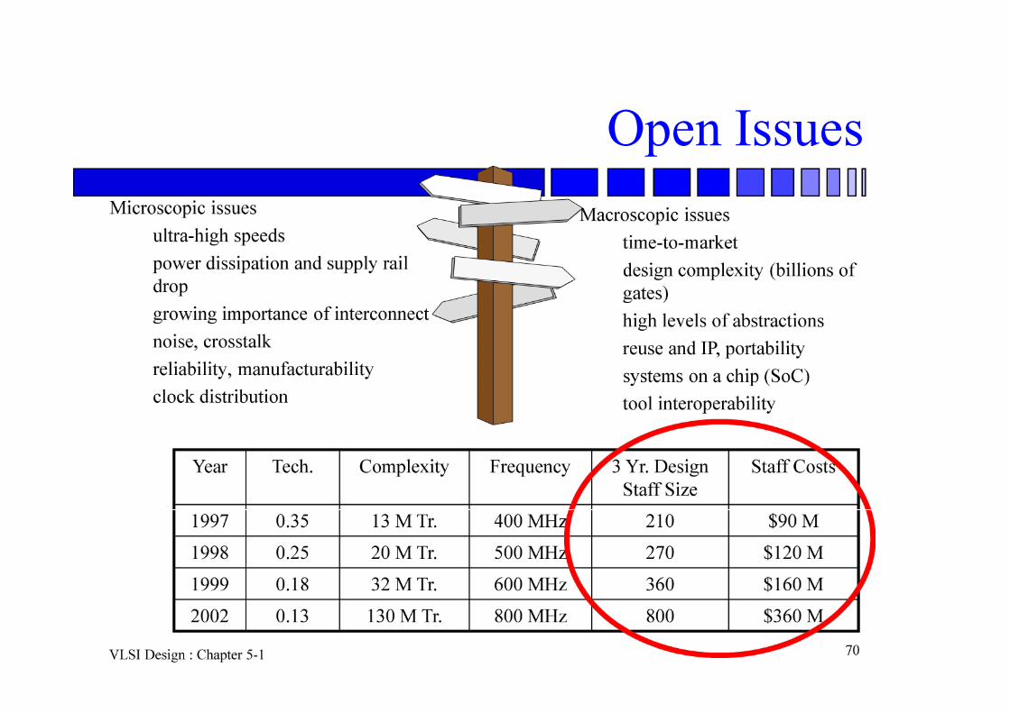
Open IssuesMicroscopic issues
ultra-high speeds
power dissipation and supply rail drop
growing importance of interconnect
noise, crosstalk
reliability, manufacturability
clock distribution
Macroscopic issues
time-to-market
design complexity (billions of gates)
high levels of abstractions
reuse and IP, portability
systems on a chip (SoC)
tool interoperability
Year Tech. Complexity Frequency 3 Yr. Design Staff Size
Staff Costs
1997 0.35 13 M Tr. 400 MHz 210 $90 M
1998 0.25 20 M Tr. 500 MHz 270 $120 M
1999 0.18 32 M Tr. 600 MHz 360 $160 M
2002 0.13 130 M Tr. 800 MHz 800 $360 M
VLSI Design : Chapter 5-1 71
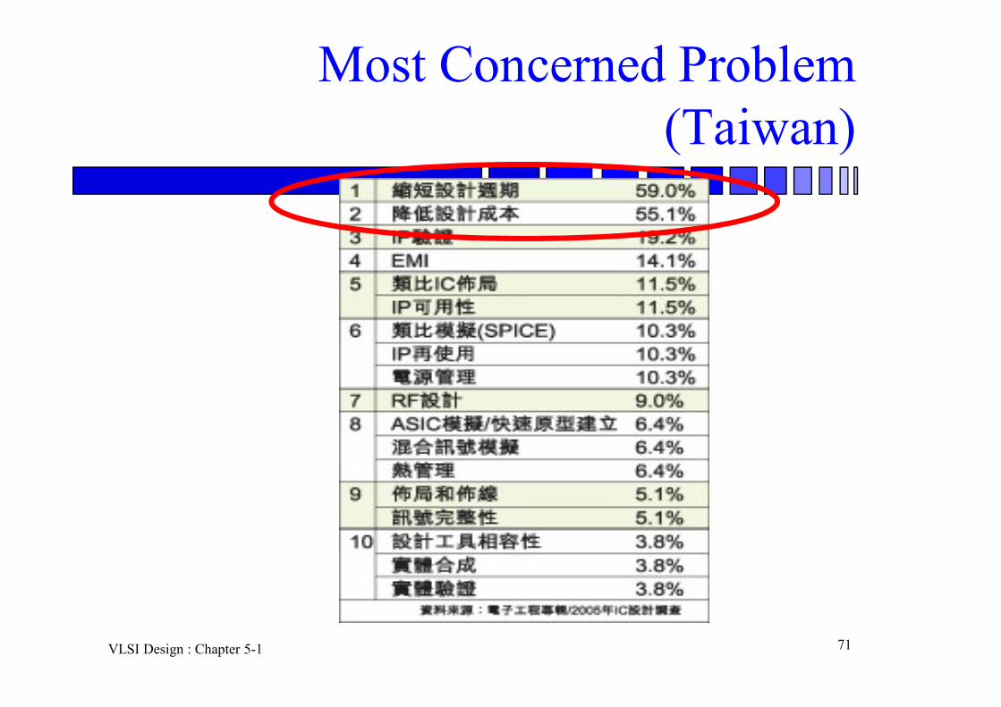
Most Concerned Problem (Taiwan)
VLSI Design : Chapter 5-1 72
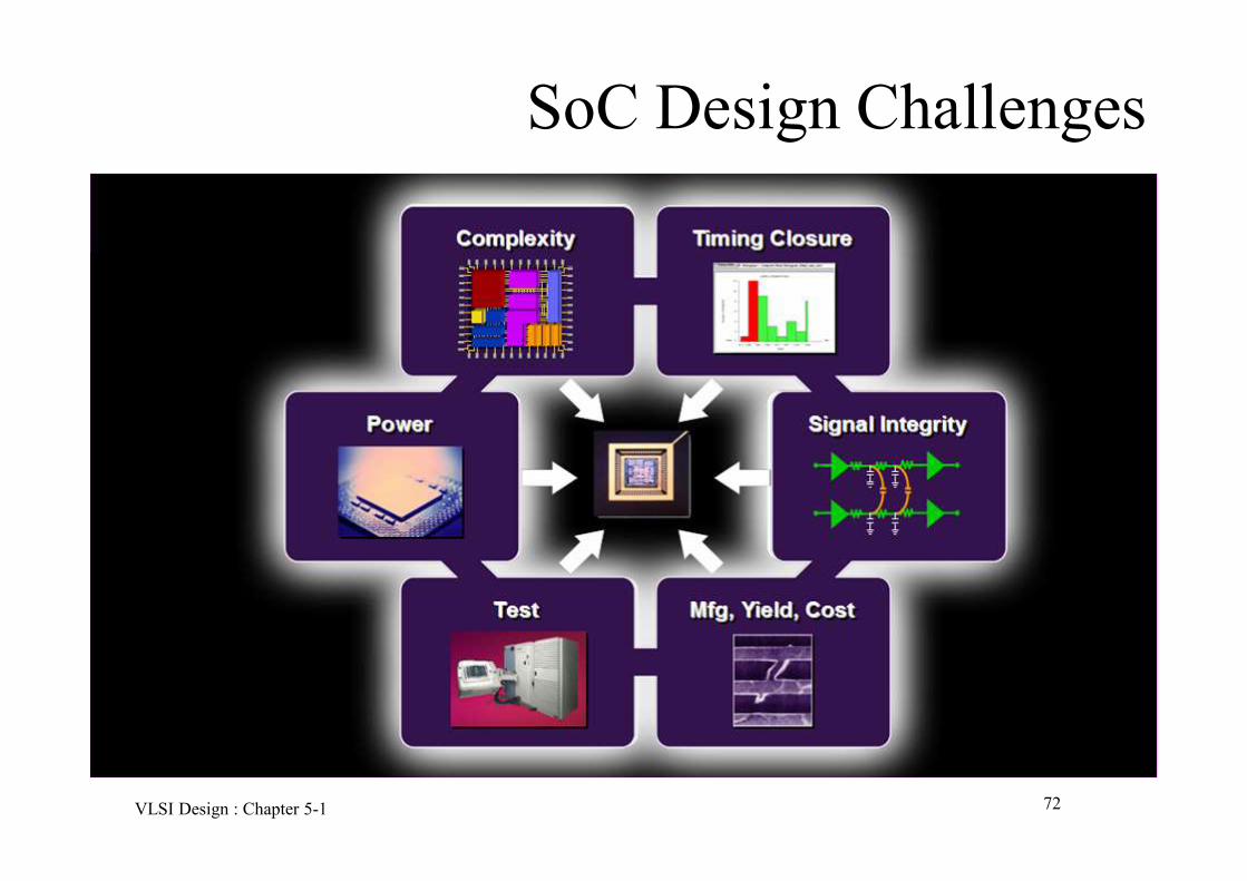
SoC Design Challenges

VLSI Design : Chapter 5-1 73
Cost !! Cost !! Cost!! Fab Cost
Cost: about $15~20 billion USD. *
Typical fab line occupies about 1 city block, employs a few hundred people.
Most profitable period is first 18 months-2 years. (This might not be true)
TSMC Fab 12
• Nicolas MokhoffSemi industry fab costs limit industry growth 10/3/2012
Fab 15 is in 台中

VLSI Design : Chapter 5-1 74
Fab Cost

VLSI Design : Chapter 5-1 75
Mask cost
Semiconductor Wafer Mask CostsSeptember 15, 2016, anysilicon
46M NTD
VLSI Design : Chapter 5-1 76
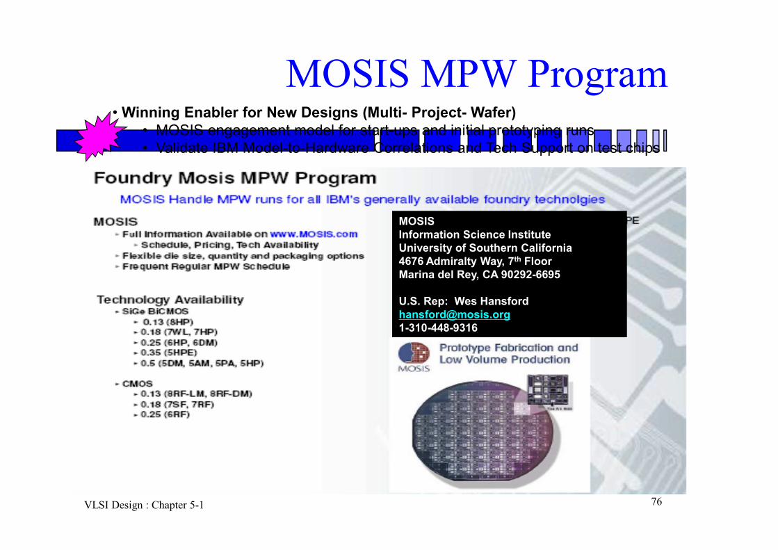
MOSIS MPW Program• Winning Enabler for New Designs (Multi- Project- Wafer)
• MOSIS engagement model for start-ups and initial prototyping runs• Validate IBM Model-to-Hardware Correlations and Tech Support on test chips
MOSISInformation Science InstituteUniversity of Southern California4676 Admiralty Way, 7th FloorMarina del Rey, CA 90292-6695
U.S. Rep: Wes [email protected]

VLSI Design : Chapter 5-1 77
2006 MOSIS MPW Schedule and Deliverables
A) MOSIS Deliverable = 40 dies per each chip designB) MOSIS MPW Pricing available at http://www.mosis.org/Orders/Prices/price-list-export.html
1. MPW Schedule for IBM: http://www.mosis.org/products/fab/schedule/ http://www.mosis.org/Orders/Prices/price-list-export.html
VLSI Design : Chapter 5-1 78
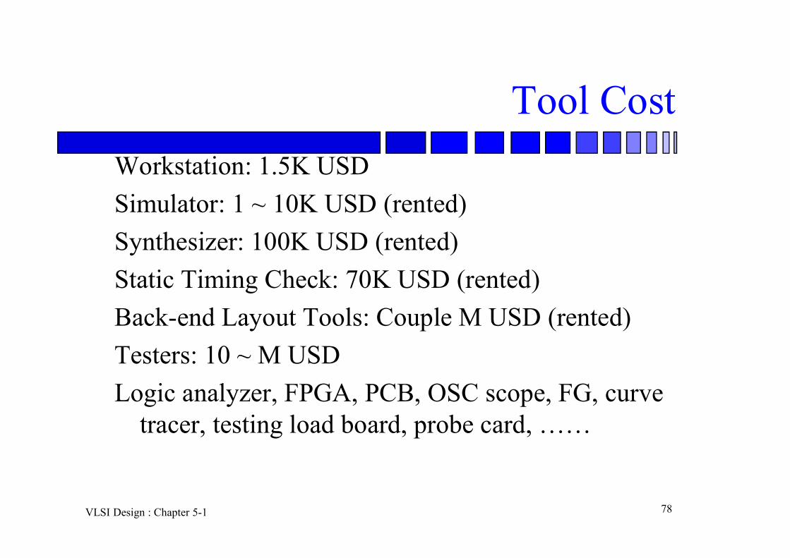
Tool Cost
Workstation: 1.5K USD
Simulator: 1 ~ 10K USD (rented)
Synthesizer: 100K USD (rented)
Static Timing Check: 70K USD (rented)
Back-end Layout Tools: Couple M USD (rented)
Testers: 10 ~ M USD
Logic analyzer, FPGA, PCB, OSC scope, FG, curve tracer, testing load board, probe card, ……
VLSI Design : Chapter 5-1 79
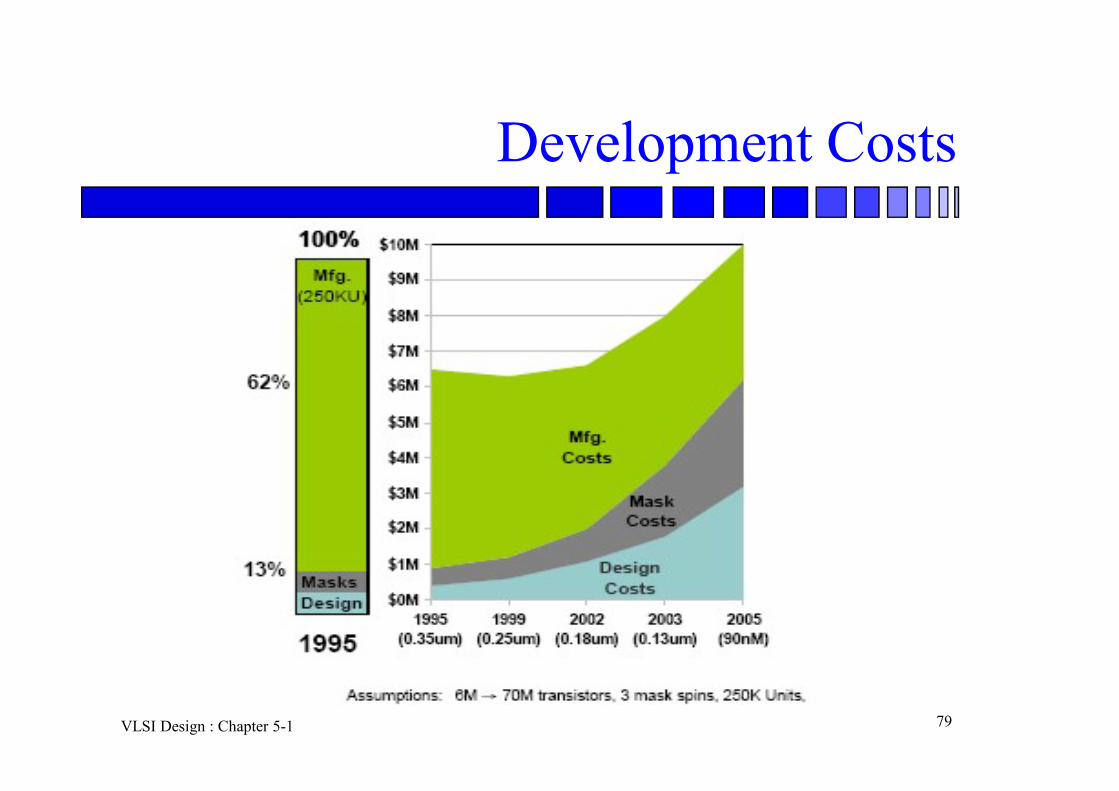
Development Costs
VLSI Design : Chapter 5-1 80
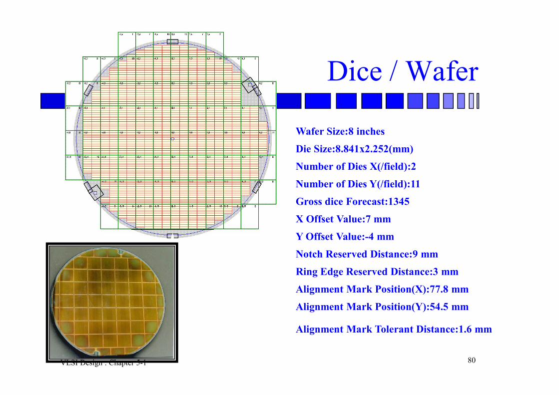
Dice / Wafer
Wafer Size:8 inches
Die Size:8.841x2.252(mm)
Number of Dies X(/field):2
Number of Dies Y(/field):11
Gross dice Forecast:1345
X Offset Value:7 mm
Y Offset Value:-4 mm
Notch Reserved Distance:9 mm
Ring Edge Reserved Distance:3 mm
Alignment Mark Position(X):77.8 mm
Alignment Mark Position(Y):54.5 mm
Alignment Mark Tolerant Distance:1.6 mm
VLSI Design : Chapter 5-1 81
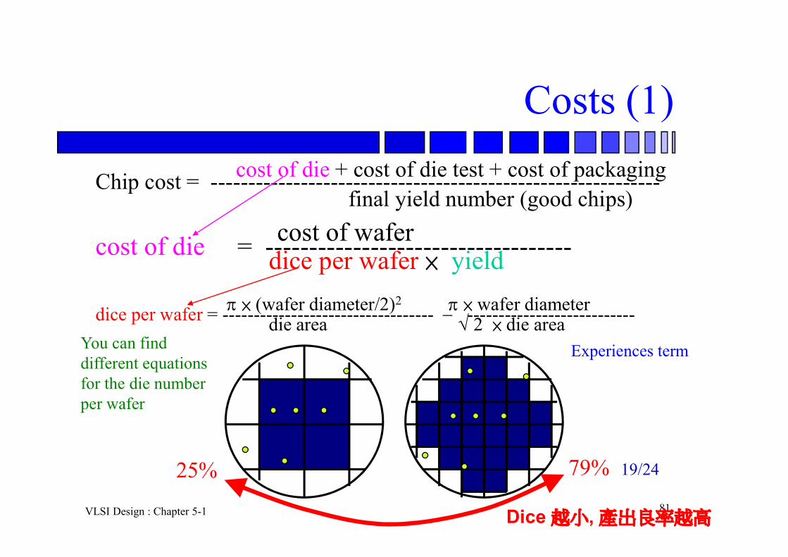
Costs (1)
cost of die + cost of die test + cost of packagingChip cost = ------------------------------------------------------------final yield number (good chips)
cost of wafercost of die = -----------------------------------dice per wafer × yield
× (wafer diameter/2)2 × wafer diameterdice per wafer = ---------------------------------- ---------------------------die area 2 × die area You can find different equations for the die number per wafer
25% 79% 19/24
Experiences term
Dice 越小, 產出良率越高

VLSI Design : Chapter 5-1 82
WaferDefects
Faulty chips
Good chips
Unclustered defectsWafer yield = 12/22 = 0.55
Clustered defects (VLSI)Wafer yield = 17/22 = 0.77
Clustered VLSI Defects
VLSI Design : Chapter 5-1 83
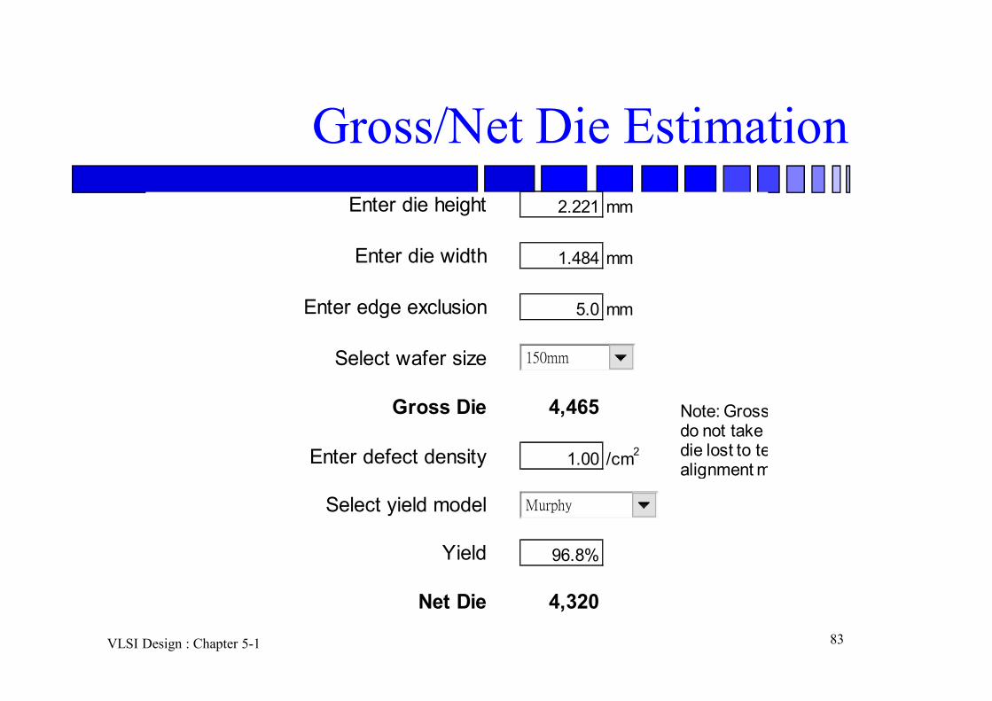
Gross/Net Die Estimation
Dice 越小, 產出良率越高
Enter die height 2.221 mm
Enter die width 1.484 mm
Enter edge exclusion 5.0 mm
Select wafer size 3
Gross Die 4,465
Enter defect density 1.00 /cm2
Select yield model 2
Yield 96.8%
Net Die 4,320
Note: Gross and net die do not take into account die lost to test sites and alignment marks.
150mm
Murphy

VLSI Design : Chapter 5-1 84
Wafer Map
Bad die
Dice 越小, 產出良率越高

VLSI Design : Chapter 5-1 85
Yield (1994)
Chip Metal layers
Line width
Wafer cost
Defects/cm2
Area (mm2)
Dies/wafer
Yield Die cost
386DX 2 0.90 $900 1.0 43 360 71% $4
486DX2 3 0.80 $1200 1.0 81 181 54% $12
PowerPC 601 4 0.80 $1700 1.3 121 115 28% $53
HP PA 7100 3 0.80 $1300 1.0 196 66 27% $73
DEC Alpha 3 0.70 $1500 1.2 234 53 19% $149
Super SPARC 3 0.70 $1700 1.6 256 48 13% $272
Pentium 3 0.80 $1500 1.5 296 40 9% $417

VLSI Design : Chapter 5-1 86
Design for Manufacturability (DFM)Approaches
1) Worst-Case Approach: choose the SPICE model giving the worst possible behavior– Traditional choice is pessimistic
and lead to circuit overdesign
(neglects any kind of correlation)
– Other techniques to choose the
SPICE model values (accounting for correlation)
2) Probability Density Function Approach: keep track of the whole distribution– Expensive: need smart ways to do it
VLSI Design : Chapter 5-1 87
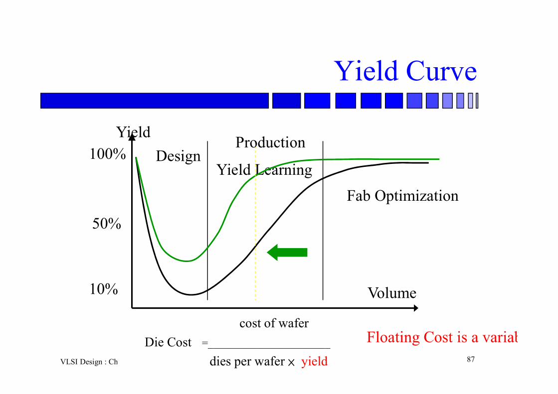
Yield Curve
100%
Volume
50%
10%
DesignYield Learning
Fab Optimization
Yield
cost of wafer
Die Cost =_______________________
dies per wafer × yield
Floating Cost is a variable!!
Production

VLSI Design : Chapter 5-1 88
Cost
Cost per IC
= Floating Cost + (Fixed Cost / Volume)
VLSI Design : Chapter 5-1 89
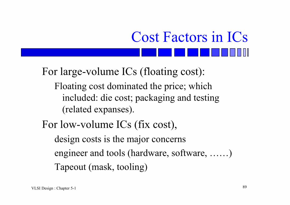
Cost Factors in ICs
For large-volume ICs (floating cost):Floating cost dominated the price; which
included: die cost; packaging and testing (related expanses).
For low-volume ICs (fix cost), design costs is the major concerns
engineer and tools (hardware, software, ……)
Tapeout (mask, tooling)
VLSI Design : Chapter 5-1 90
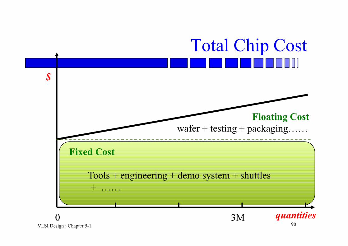
Total Chip Cost
quantities0 3M
$
Tools + engineering + demo system + shuttles+ ……
wafer + testing + packaging……
Fixed Cost
Floating Cost
VLSI Design : Chapter 5-1 91
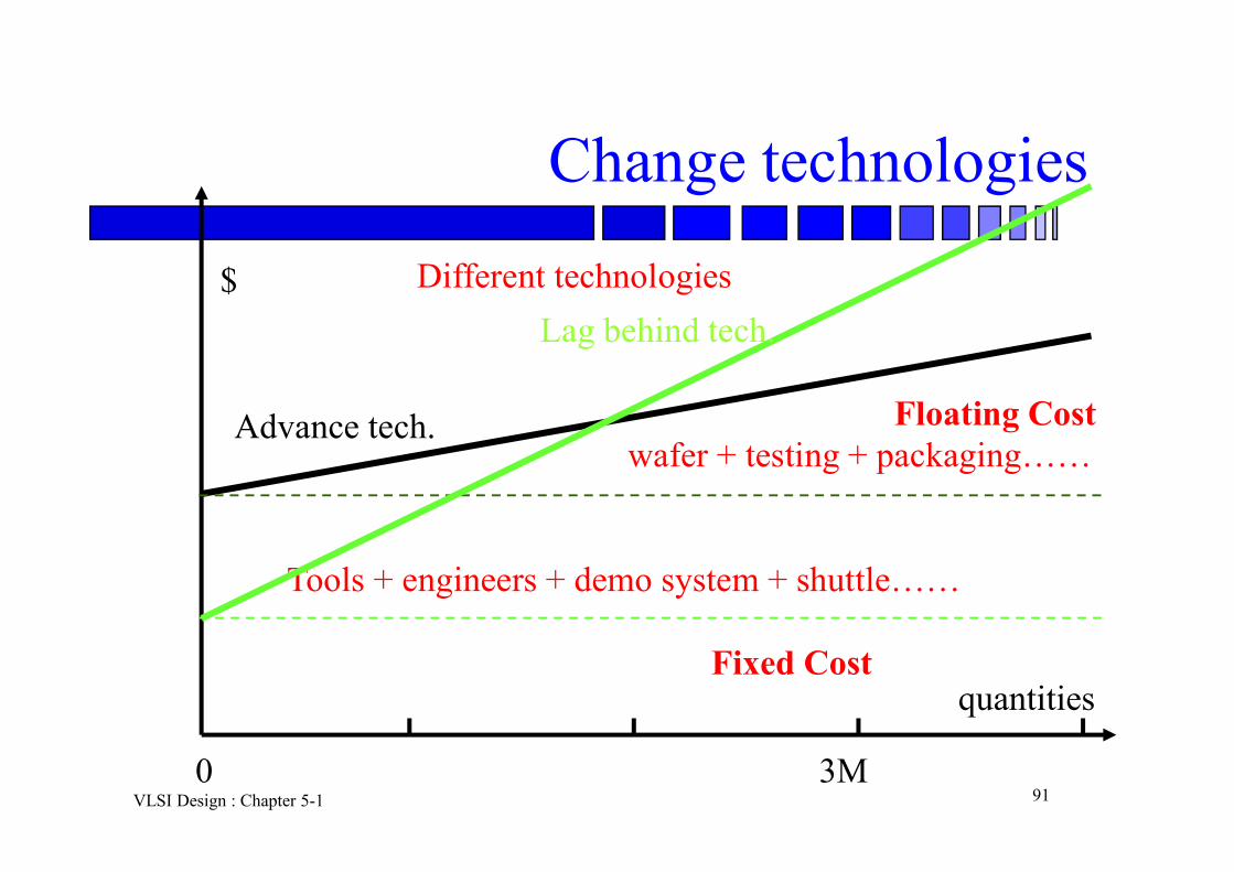
Change technologies
quantities
0 3M
$
Tools + engineers + demo system + shuttle……
wafer + testing + packaging……
Fixed Cost
Floating Cost
Different technologies
Advance tech.
Lag behind tech.

VLSI Design : Chapter 5-1 92
Sales vs. Costs
quantities
0 3M
$
Fix Cost
Floating Cost
Sales revenueCompany A
Balance point
loss
profit

VLSI Design : Chapter 5-1 93
Competitions
quantities
0 3M
$ Sales revenue
Delay
Company A
Company B
Sales revenue
VLSI Design : Chapter 5-1 94
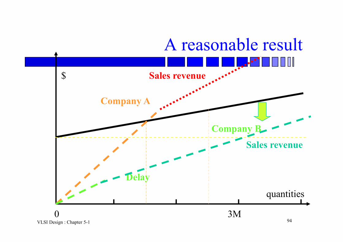
A reasonable result
quantities
0 3M
$ Sales revenue
Delay
Company A
Company B
Sales revenue

VLSI Design : Chapter 5-1 95
Flow
Marketing surveySpecification
Design: Architecture, Logic, Circuit
Backend, ….
Testing
Manufacture:Masks, Die, Packaging
Market

VLSI Design : Chapter 5-1 96
Design Cycle
Specification: function, cost, market window, etc.
Architecture: large blocks partition
Logic: gates + registers (memories)
Circuits: transistors, sizes for speed, power…
Backend design: Put the circuit on silicon, determines parasitics
Manufacture
Testing
VLSI Design : Chapter 5-1 97
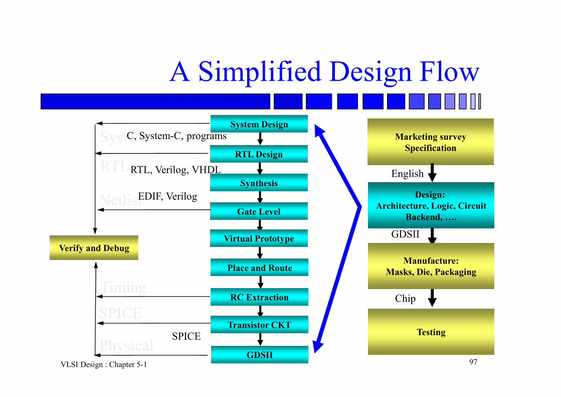
A Simplified Design Flow
System Design
Verify and Debug
Synthesis
Gate Level
Virtual Prototype
Place and Route
RC Extraction
Transistor CKT
GDSII
RTL Design
System
RTL
Netlist
Timing
Physical
SPICE
Marketing surveySpecification
Design: Architecture, Logic, Circuit
Backend, ….
Testing
Manufacture:Masks, Die, Packaging
English
C, System-C, programs
EDIF, Verilog
SPICE
RTL, Verilog, VHDL
Chip
GDSII

VLSI Design : Chapter 5-1 98
Design Validation
Must check at every step that errors haven’t been introduced-the longer an error remains, the more expensive it becomes to remove it.
Forward checking: compare results of less-and more-abstract stages.
Back annotation: copy performance numbers to earlier stages.
VLSI Design : Chapter 5-1 99
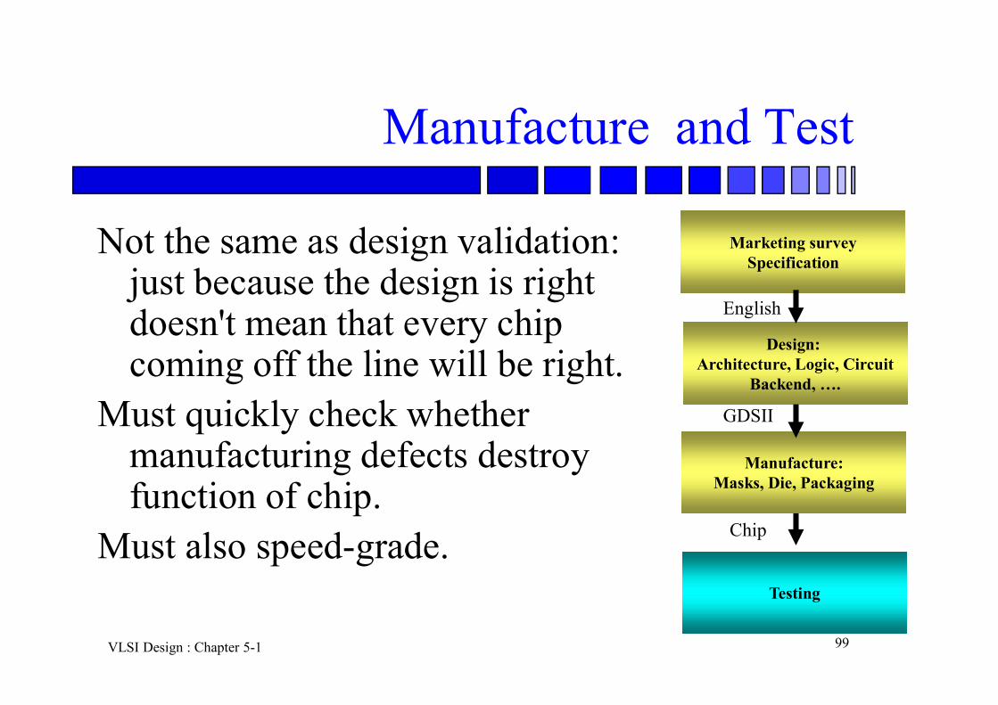
Manufacture and Test
Not the same as design validation: just because the design is right doesn't mean that every chip coming off the line will be right.
Must quickly check whether manufacturing defects destroy function of chip.
Must also speed-grade.
Marketing surveySpecification
Testing
Design: Architecture, Logic, Circuit
Backend, ….
Manufacture:Masks, Die, Packaging
English
Chip
GDSII

VLSI Design : Chapter 5-1 100
Company Size
VLSI Design : Chapter 5-1 101
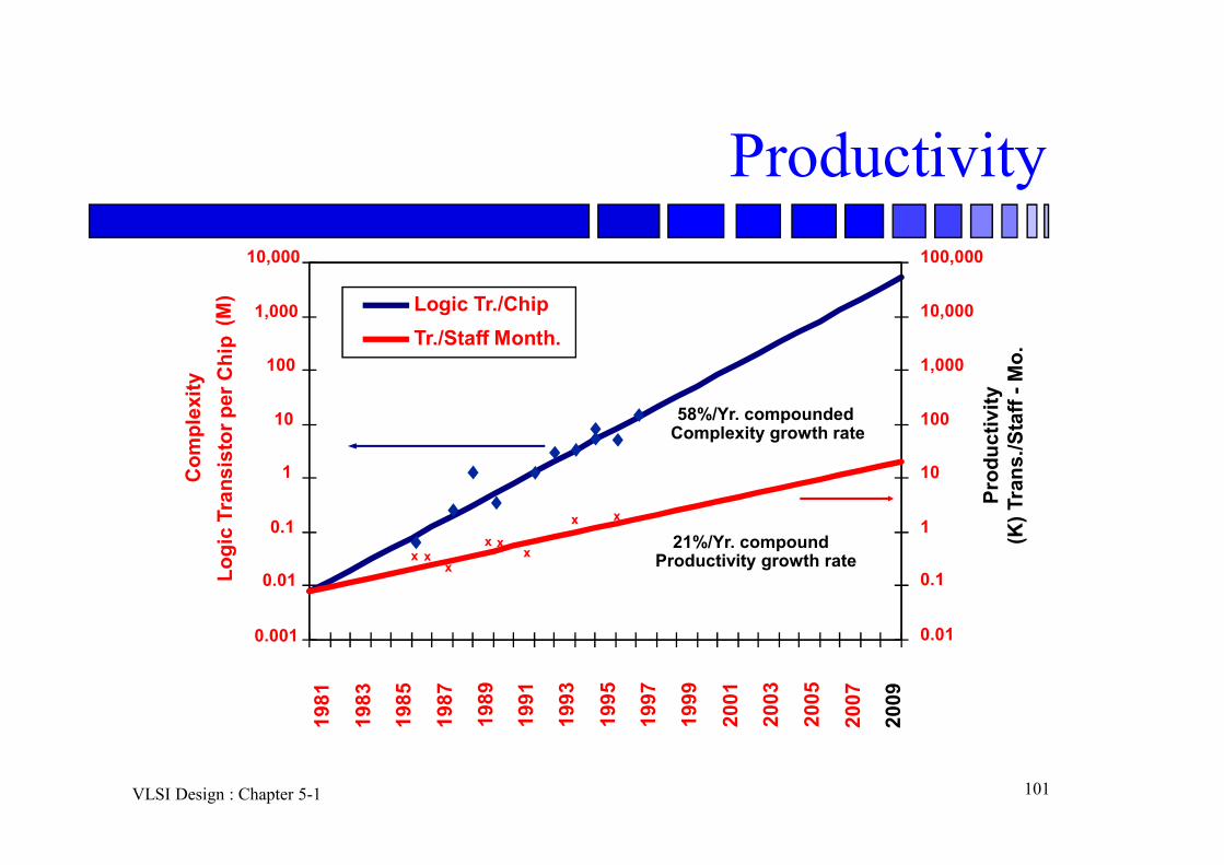
Productivity
200
3
198
1
198
3
198
5
198
7
198
9
199
1
199
3
199
5
199
7
199
9
200
1
200
5
200
7
200
9
Logic Tr./Chip
Tr./Staff Month.
xxx
xxx
x
21%/Yr. compoundProductivity growth rate
x
58%/Yr. compoundedComplexity growth rate
10,000
1,000
100
10
1
0.1
0.01
0.001
Lo
gic
Tra
ns
isto
r p
er C
hip
(M)
0.01
0.1
1
10
100
1,000
10,000
100,000
Pro
du
cti
vity
(K)
Tran
s./S
taff
-M
o.
Co
mp
lexi
ty

VLSI Design : Chapter 5-1 102
The mythical man-monthThe situation is even worse than the productivity gap indicatesIn theory, adding designers to team reduces project completion timeIn reality, productivity per designer decreases due to complexities of team
management and communication In the software community, known as “the mythical man-month” (Brooks 1975)At some point, can actually lengthen project completion time! (“Too many cooks”)
10 20 30 400
10000
20000
30000
40000
50000
60000
43
24
1916 15 16
18
23
Team
Individual
Months until completion
Number of designers
1M transistors, 1 designer=5000 trans/month
Each additional designer reduces for 100 trans/month
So 2 designers produce 4900 trans/month each

VLSI Design : Chapter 5-1 103
Time to Market
VLSI Design : Chapter 5-1 104
Time to MarketR
even
ues
($)
Time (months)
On-time Delayedentry entry
Peak revenue
Peak revenue from delayed entry
Market rise Market fall
TimeD
On-time
Delayed
Rev
enue
s ($
)
Cos
ts (
$)
Quantities (M)
VLSI Design : Chapter 5-1 105
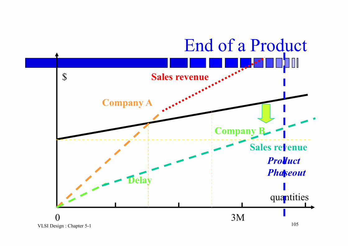
End of a Product
quantities
0 3M
$ Sales revenue
Delay
Company A
Company B
Sales revenueProductPhaseout
VLSI Design : Chapter 5-1 106
Conclusions
It’s a very tough business!!

VLSI Design : Chapter 5-1 107
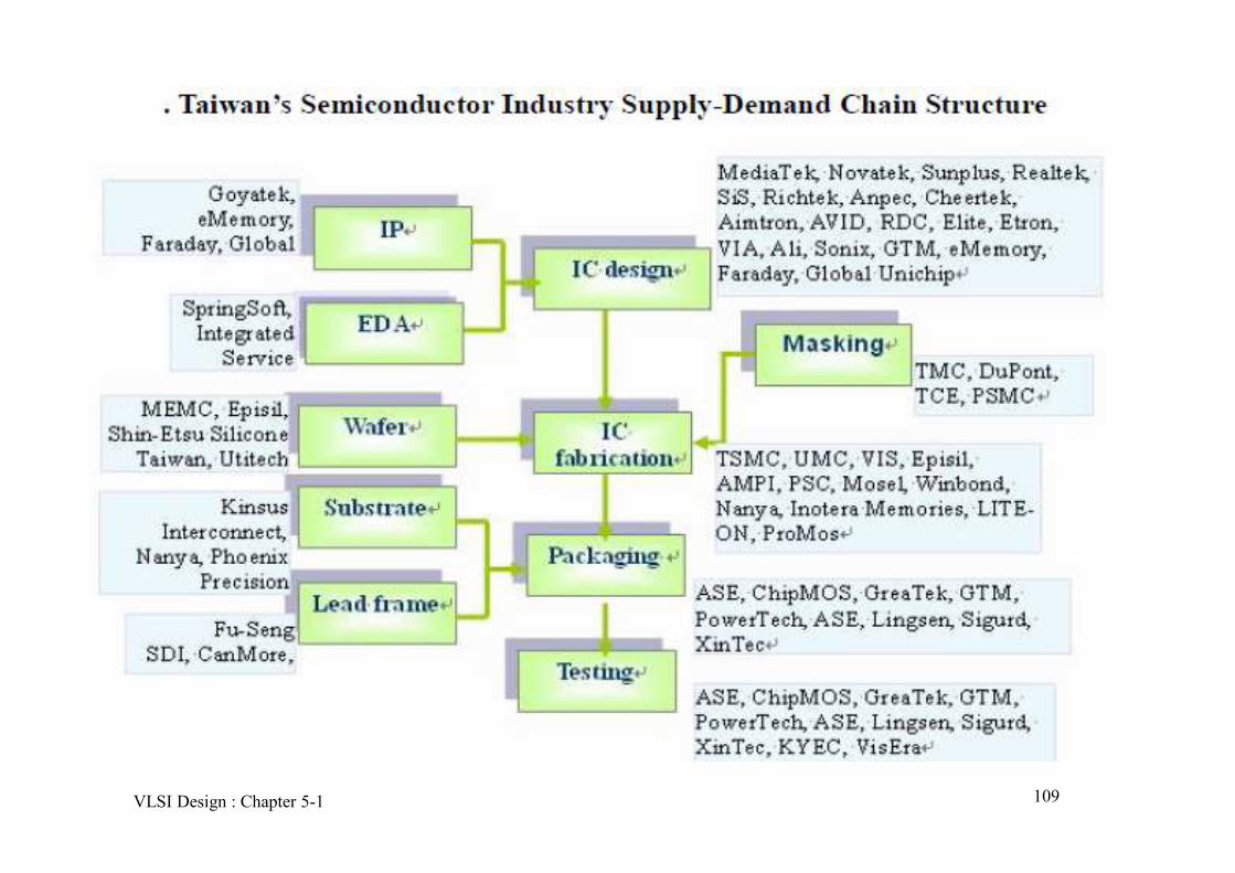
Semiconductor Industry Segments
Design Houses: Fabless: Broadcomm, Xilinx, PMCS, nVedia, (300+ in SV)… SunPlus, MediaTek, (250+ in TW)… IP Vendors: ARM, MIPS, eMemory, …
Pure Foundries: TSMC, UMC, Chartered, …CAD: Synopsys/Avant!, Cadence, Mentor Graphics,
… Syntest, Spring Soft/NOVAPackaging: ASE (日月光), Amkor, Equipment: Applied Material. HP, LAM

VLSI Design : Chapter 5-1 108
Relationship
VLSI Design : Chapter 5-1 109
VLSI Design : Chapter 5-1 110
IC Design House
(Fabless)
IP Provider (Chipless)Provide IP blocksPre-design + pre-simulation = Reuse IP
EDA Tools (CAD)Electronic Design Automation
Design Services CompanyFaraday, GoYa, Socle, InnoChip, GlobalUniChip, GlobalCAD, Arcadia(Provide IP , P&R, backend service
Packaging / TestingASE / 矽品 / 華泰
(Packaging)福雷電/矽豐/南茂 (Testing)
Consumer、Controller 、Network / Communication 、Computer IC
Fab --- TSMC / UMC / Charter / SamSung / 中芯SMIC / HJ / Tower / Epsil / OKI / …0.09um, .13, .15, 18, .25, .35, .5, .8, 1.0… 6.0
Equipment / IDE (Integrated Design Equipment)台灣應用材料 Apply Material…..
IDM / Integrated Device ManufacturerIntel / IBM/ NEC/ TI /NS/Motorola/ST/Winbond/ Hitachi/NS/Sony/Samsung/LSI Logic/Philips(EDA) +IC Design + Foundry + (System) 從事自有品牌的IC設計/製造/銷售,並擁有雄厚資金及生產能力
晶圓委外代工釋放Foundry
Distributor零組件通路商世平、大騰、宏碁、友尚、聯強、品佳、威健、宇詮、詮鼎、文曄
Manufacture / System House台達電、宏碁、華碩、廣達…Dell, HP, TRW, Raytheon, Rockwell, Hughes
Software / Consultant / Solution Provider
Cadence / Synopsys; Avant! / Altera / Xilinx / Mentor Graphics / Nova / Syntest/IKOS/QuickTurn茂積 / 茂綸 / 美商新思 / 宏太 / 翌傑
RISC / ARM; MIPS, TTPCOMASIC / 智原-創意-巨有-荃文-科雅-美商新思Memory: Virage, DophlinAnalog Blocks…
威盛
揚智
凌揚
鈺創
聯發
聯詠
美商智霖
創品電子
義隆
金麗半導體IC
SI, Sun, nVidia
Xilinx, S3, A
TI, A
MD
, B roadC
OM
M, Q
ualcomm
, PM
CS
VLSI Design : Chapter 5-1 111
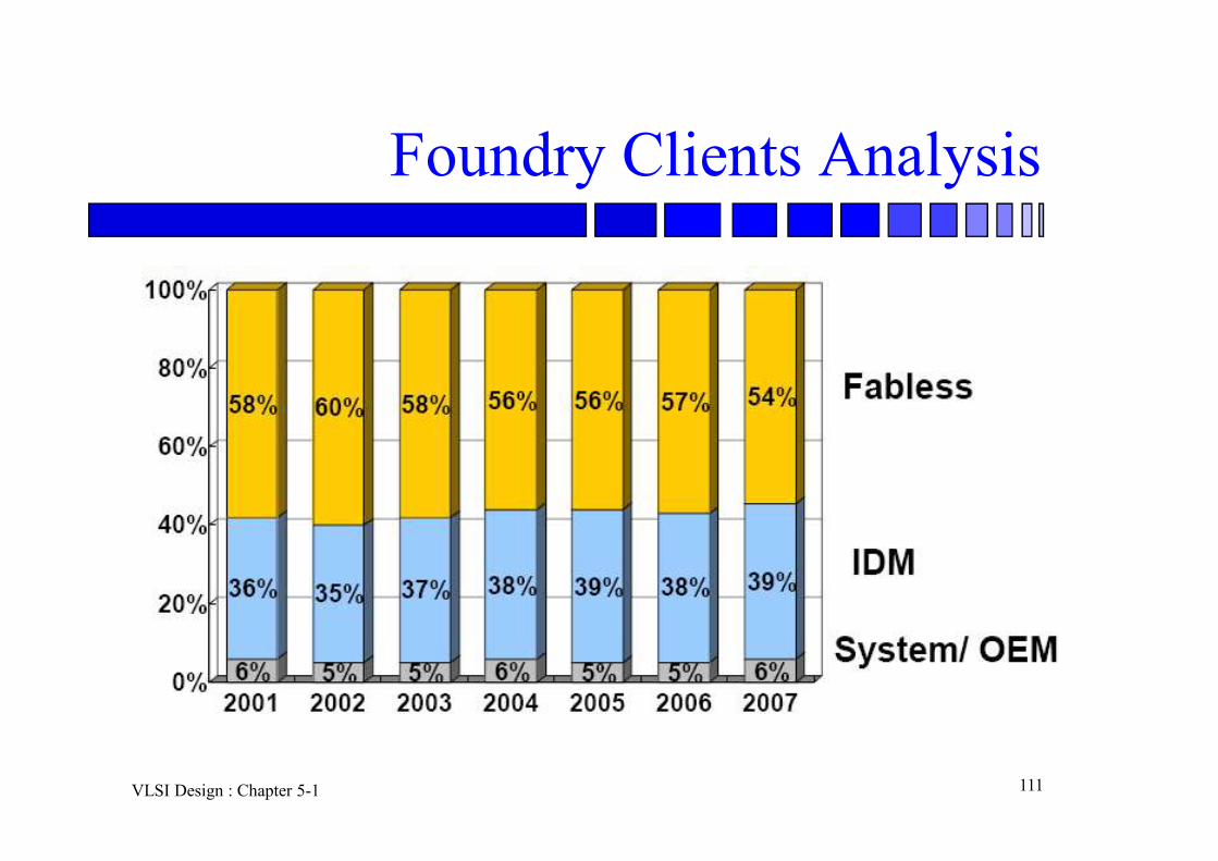
Foundry Clients Analysis
VLSI Design : Chapter 5-1 112
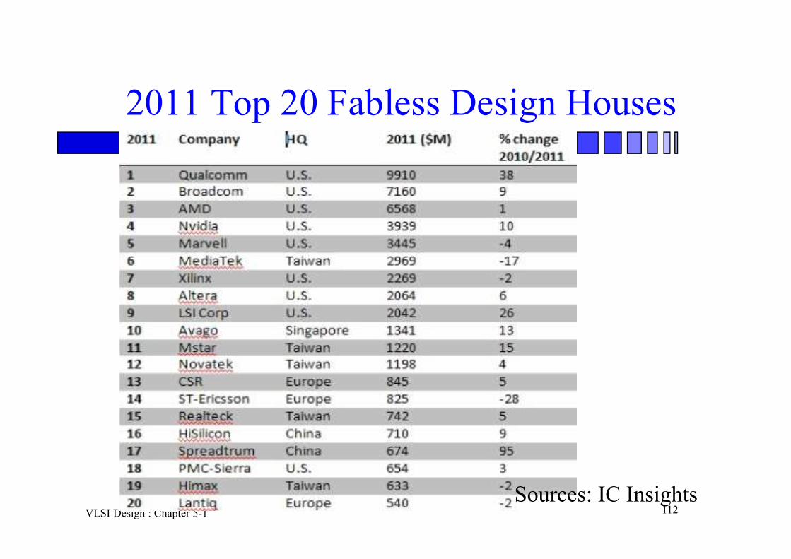
2011 Top 20 Fabless Design Houses
Sources: IC Insights
VLSI Design : Chapter 5-1 113
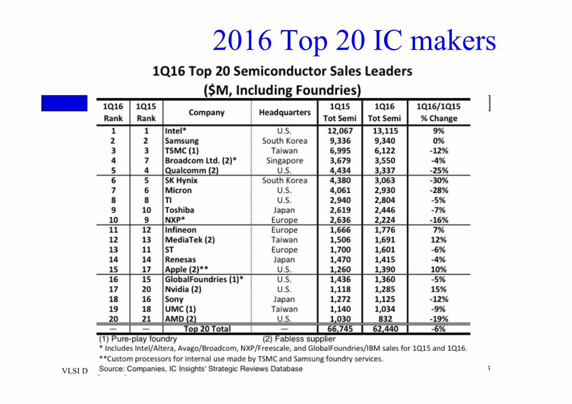
2016 Top 20 IC makers
VLSI Design : Chapter 5-1 114
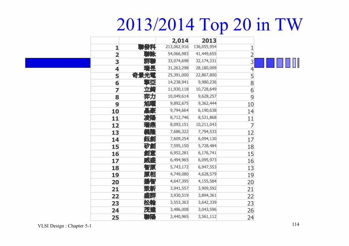
2013/2014 Top 20 in TW2,014 2013
1 聯發科 213,062,916 136,055,954 12 聯詠 54,066,983 41,449,655 23 群聯 33,074,698 32,174,331 34 瑞昱 31,263,298 28,180,009 45 奇景光電 25,391,000 22,867,800 56 擎亞 14,238,941 9,980,236 87 立錡 11,930,118 10,728,649 68 弈力 10,049,614 9,628,257 99 旭曜 9,892,675 9,362,444 10
10 晶豪 9,794,664 6,190,638 1411 凌陽 8,712,746 8,521,868 1112 瑞鼎 8,093,151 10,211,043 713 義隆 7,686,322 7,794,533 1214 鈺創 7,609,254 6,094,130 1715 矽創 7,595,150 5,728,484 1816 創意 6,952,281 6,176,741 1517 威盛 6,494,965 6,095,973 1618 智原 5,743,172 6,947,553 1319 原相 4,749,080 4,628,579 1920 揚智 4,647,395 4,155,584 2021 致新 3,941,557 3,909,592 2122 盛群 3,930,519 3,894,361 2223 松翰 3,553,363 3,642,339 2324 茂達 3,486,008 3,043,596 2625 聯陽 3,440,965 3,561,112 24

VLSI Design : Chapter 5-1 115
2013~15 Top Packaging Houses
VLSI Design : Chapter 5-1 116
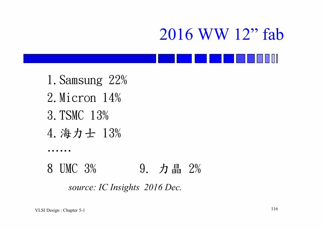
2016 WW 12” fab
1.Samsung 22%
2.Micron 14%
3.TSMC 13%
4.海力士 13%
……
8 UMC 3% 9. 力晶 2%
source: IC Insights 2016 Dec.

VLSI Design : Chapter 5-1 117
Taiwan vs. China
VLSI Design : Chapter 5-1 118
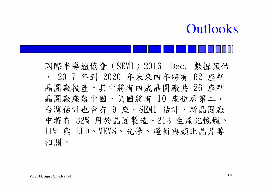
Outlooks
國際半導體協會(SEMI)2016 Dec. 數據預估, 2017 年到 2020 年未來四年將有 62 座新晶圓廠投產,其中將有四成晶圓廠共 26 座新晶圓廠座落中國,美國將有 10 座位居第二,台灣估計也會有 9 座。SEMI 估計,新晶圓廠中將有 32% 用於晶圓製造、21% 生產記憶體、11% 與 LED、MEMS、光學、邏輯與類比晶片等相關。

VLSI Design : Chapter 5-1 119
Taiwan
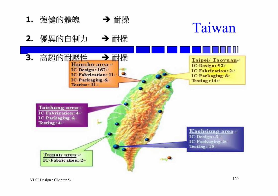
VLSI Design : Chapter 5-1 120
Taiwan