3D PRINTED SPATIALLY VARIANT ANISOTROPIC...
110
3D PRINTED SPATIALLY VARIANT ANISOTROPIC METAMATERIALS CESAR ROMAN GARCIA Department of Electrical and Computer Engineering APPROVED: Raymond Rumpf, Ph.D., Chair Joseph Pierluissi, Ph.D. Virgilio Gonzalez, Ph.D. Helmut Knaust, Ph.D. Bess Sirmon-Taylor, Ph.D. Interim Dean of the Graduate School
Transcript of 3D PRINTED SPATIALLY VARIANT ANISOTROPIC...

3D PRINTED SPATIALLY VARIANT
ANISOTROPIC METAMATERIALS
CESAR ROMAN GARCIA
Department of Electrical and Computer Engineering
APPROVED:
Raymond Rumpf, Ph.D., Chair
Joseph Pierluissi, Ph.D.
Virgilio Gonzalez, Ph.D.
Helmut Knaust, Ph.D.
Bess Sirmon-Taylor, Ph.D.
Interim Dean of the Graduate School

Copyright ©
by
Cesar Roman Garcia
2014
3D PRINTED SPATIALLY VARIANT
ANISOTROPIC METAMATERIALS
by
CESAR ROMAN GARCIA, BSEP
DISSERTATION
Presented to the Faculty of the Graduate School of
The University of Texas at El Paso
in Partial Fulfillment
of the Requirements
for the Degree of
DOCTOR OF PHILOSOPHY
Department of Electrical and Computer Engineering
THE UNIVERSITY OF TEXAS AT EL PASO
May 2014

iv
Acknowledgements
Primarily, I would like to thank my family for their support during my graduate studies.
Thank you to my wife, Dalia, who put up with a husband in graduate school, my parents, Mom
and Dad, for always supporting me, and my son, Cesar Rene, who I have spent so much time
away from.
Thank you to my advisor, Dr. Raymond Rumpf (Tipper), for mentoring and teaching me
during this process of obtaining my Ph.D. I have learned a great deal from you. Also, I would
like to thank my committee members for their time and their contributions: Dr. Virgilio
Gonzalez, Dr. Joseph Pierluissi, and Dr. Helmut Knaust.
Thank you to Dr. Benjamin Flores, Dr. Helmut Knaust, and Mrs. Ariana Arciero-Pino. I
am extremely grateful for your advice and for receiving the NSF Bridge to Doctorate Fellowship.
Finally, I would like to acknowledge my work wife, J.H.B., there will always be a filing
cabinet in between us.
v
Abstract
The recent advancement in 3D printing has created a new way to design electronics and
electromagnetic devices. This allows for a new breed of non-planar designs to be used, fully
exploiting all three dimensions like never before. More functions can be fit into the same
amount of space, products with novel form factors can be more easily manufactured,
interconnects can be routed more smoothly, interfaces can be better implemented, electrical and
mechanical functions can be comingled, and entirely new device paradigms will be invented.
When departing from traditional planar topologies many new problems arise like signal integrity,
crosstalk, noise, and unintentional coupling between devices. The primary focus of this
dissertation is to demonstrate that spatially variant anisotropic metamaterials (SVAM’s) are a
viable solution to alleviate those unwanted problems. Currently, there are no solutions to fix
these problems in a fully 3D device, but there have been numerous efforts to alleviate those
problems in traditional devices. Those solutions often use metals that introduce unwanted loss
and require extra space to be added to the device. SVAM’s do not introduce significant loss,
since they are all-dielectric, and better accommodate systems that have size restraints.
To be able to design and model SVAM’s, six numerical tools were formulated and
implemented. In addition, one commercial software package was used.
First, a design methodology was developed for generating an all-dielectric metamaterial
with a specific dielectric tensor. Next, a microstrip transmission line was isolated from a metal
object placed in close proximity by embedding it in a SVAM so that the field avoided the object.
Next, the electromagnetic impact of the typical surface roughness in metal parts produced by 3D
print metals was evaluated. Finally, a SVAM was built into a cell phone case to minimize the
interaction of two cell phone antennas in close proximity.
vi
Table of Contents
Acknowledgements .................................................................................................................. iv
Abstract ......................................................................................................................................v
Table of Contents ..................................................................................................................... vi
List of Tables ......................................................................................................................... viii
List of Figures .......................................................................................................................... ix
Chapter 1: Introduction ..............................................................................................................1
1.1 Overview of Dissertation .........................................................................................1
1.2 3D Printing ...............................................................................................................2
1.3 Anisotropic Materials...............................................................................................5
1.4 Electromagnetic Metamaterials ...............................................................................5
1.5 State-of-the-Art in Electromagnetic Isolation ..........................................................7
Chapter 2: Numerical Tools .....................................................................................................10
2.1 Ansys® HFSS ........................................................................................................10
2.2 4 4 Transfer Matrix Method for Anisotropic Materials (ATMM) .......................10
2.3 2D Plane Wave Expansion Method .......................................................................20
2.4 Finite-Difference Analysis of Arbitrary Transmission Lines Embedded in
Anisotropic Media .................................................................................................23
2.5 Anisotropic Finite-Difference Frequency-Domain Method ..................................31
2.6 Tool for Synthesizing Spatially Variant Lattices ...................................................42
2.7 Transformation Optics ...........................................................................................47
Chapter 3: 3D Printing of Anisotropic Metamaterials .............................................................54
3.1 Device Design ........................................................................................................54
3.2 Experimental Results .............................................................................................57
3.3 Conclusions ............................................................................................................60
Chapter 4: Electromagnetic Isolation of A Microstrip by Embedding in a Spatially Variant
Anisotropic Metamaterial ...............................................................................................61
4.1 Microstrip embedded in anisotropic media............................................................61
4.2 Device Design ........................................................................................................63
4.3 Experimental Results .............................................................................................66

vii
4.4 Conclusions ............................................................................................................70
Chapter 5: Effects of Extreme Surface Roughness on a 3D Printed Horn Antenna ...............71
5.1 Device and Manufacturing .....................................................................................71
5.2 Experimental Results .............................................................................................73
5.4 Conclusions ............................................................................................................75
Chapter 6: Electromagnetic Isolation of Cell Phone Antennas by Embedding in a Spatially
Variant Anisotropic Metamaterial ..................................................................................76
6.1 Envelope Correlation Coefficient ..........................................................................76
6.2 Cell Phone Antenna Design ...................................................................................77
6.3 Effects of Second Antenna .....................................................................................79
6.4 SVAM Design ........................................................................................................82
6.5 SVAM Reduction of ECC .....................................................................................84
6.6 Conclusions ............................................................................................................85
Chapter 7: Conclusions ............................................................................................................86
7.1 Conclusions ............................................................................................................86
7.2 Suggestion for Future Work...................................................................................87
References ................................................................................................................................89
Appendix ..................................................................................................................................93
A1 Derivation of Expression for Scattering Parameters ..............................................93
A2 Derivation of Redheffer Star Product ....................................................................97
Vita… .......................................................................................................................................99

viii
List of Tables
Table 5.1.1: Measured lengths of horn antennas ......................................................................... 73 Table 5.1.2: Simulated and measured gain at 15 GHz at normal incidence ................................ 73 Table 6.6.1: ECC.......................................................................................................................... 85

ix
List of Figures
Figure 1.2.1: Illustration of FDM machine [8] ............................................................................... 3 Figure 1.2.2: Illustration for SL machine [9] .................................................................................. 4 Figure 1.2.3: Illustration of EBM machine [11] ............................................................................ 4 Figure 1.4.1: Sub-sections of engineered materials [12] ................................................................ 6 Figure 1.4.2: Photonic Band Diagram of light lines and real bands [12] ...................................... 7
Figure 1.5.1: State-of-the-Art in microstrip isolation ..................................................................... 8 Figure 1.5.2: State-of-the-Art in antenna isolation ........................................................................ 9 Figure 2.2.1: 3D to 1D homogenization [12] ............................................................................... 11 Figure 2.2.2: Geometry of an embedded layer [12] ...................................................................... 18 Figure 2.4.1: 4×4 grid for the finite-difference solution to Eq. (2.80) .......................................... 26
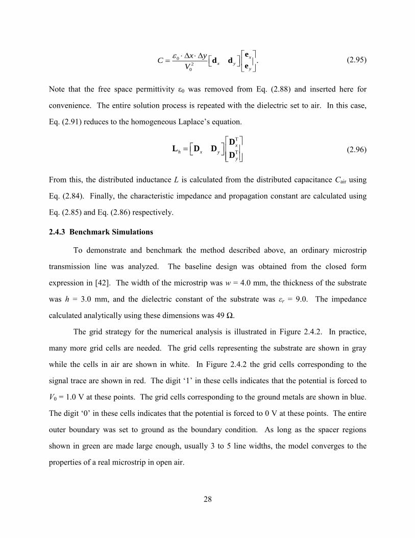
Figure 2.4.2: Grid strategy for finite-difference analysis of a microstrip transmission line ......... 29 Figure 2.4.3: Four arrays describing the distribution of dielectric ............................................... 30
Figure 2.4.4: Numerical results for an ordinary microstip ........................................................... 30 Figure 2.5.1 3D Yee cell along with position of the tensor elements ........................................... 34
Figure 2.5.2: Anisotropic GMR filter spectral response simulated with Ansys HFSS b)
Anisotropic GMR spectral response simulated with AFDFD ...................................................... 41
Figure 2.5.3: Prototype of anisotropic GMR filter ...................................................................... 42 Figure 2.6.1: Metamaterial unit cell and its constituent 1D gratings [12] ................................... 43 Figure 2.6.2: Direction field and resulting spatially variant lattice [12] ....................................... 44
Figure 2.6.3: Lattice period field and resulting spatially variant lattice [12] ............................... 44 Figure 2.6.4.: Correct method for generating spatially variant 1D gratings [12] ......................... 46
Figure 2.7.1: Example of coordinate transformation [12] ............................................................ 48 Figure 2.7.2: Material parameters for a far-zone lens .................................................................. 51
Figure 2.7.3: Simulated far zone lens using AFDFD.................................................................... 51 Figure 2.7.4: Material Parameters of Cloak .................................................................................. 52
Figure 2.7.5: AFDFD simulation of cloak ................................................................................... 53 Figure 3.1.1: Pictures or various unit cells simulated ................................................................... 56 Figure 3.1.2: Double Parameter Sweep of Anisotropic Unit Cell ................................................ 57
Figure 3.2.1: Manufactured Anisotropic Metamaterials ............................................................... 58
Figure 3.2.2: Materials under test. (Top) Rods in the z-direction. (Middle) Rods in the y-
direction. (Bottom) Rods in the x-direction .................................................................................. 59 Figure 3.2.3: Measured dielectric tensor ....................................................................................... 60 Figure 4.1.1: Study on the effect of the strength of the anisotropy of the surrounding medium . 61 Figure 4.1.2: Study on the effect of the strength of spatially varying the anisotropy of the
surrounding medium ..................................................................................................................... 62
Figure 4.1.3: Rigorous 3D simulation of standard microstrip transmission line with and without a
metal ball placed in close proximity. ............................................................................................ 63 Figure 4.1.4: Rigorous 3D simulation of standard microstrip transmission line with and without
a metal ball placed in close proximity. ......................................................................................... 63 Figure 4.2.1: Cross section of the unit cell. For εr1 = 40 and εr2 = 2.33, the optimized ratio d/a is
0.8.................................................................................................................................................. 65
Figure 4.2.2: SVAM to be placed on top of an otherwise ordinary microstrip ............................ 65 Figure 4.2.3: Orientation of the anisotropy of the SVAM ............................................................ 66 Figure 4.3.1: 3D printed spatially variant anisotropic metamaterial ............................................ 67

x
Figure 4.3.2: SVAM packed with TiO2 nano-powder .................................................................. 68
Figure 4.3.3: Microstrip transmission line in test setup, with and without the SVAM in place ... 68 Figure 4.3.4: Reflection from the bare microstrip, with and without the SVAM in place ........... 69 Figure 4.3.5: Change in S11 as ball is placed and removed for two cases: (1) solid blue line is for
the microstrip in air, and (2) dashed red line is for the microstrip embedded in the SVAM. ....... 70 Figure 5.1.1: (a) Reference horn, (b) 3D printed horn #1, (c) 3D printed horn #2. ...................... 71 Figure 5.1.2: Geometry of horn antennas ..................................................................................... 72 Figure 5.2.1: Experimental Setup ................................................................................................ 74 Figure 5.2.2: Measured transmission ............................................................................................ 74
Figure 6.1.1: One IFA design ...................................................................................................... 77 Figure 6.1.2: Simulated IFA ......................................................................................................... 78 Figure 6.2.3: 3D field radiation pattern of IFA at 740 MHz........................................................ 79 Figure 6.3.1: Two IFA design ...................................................................................................... 80
Figure 6.3.2: Simulated two antenna design ................................................................................. 80 Figure 6.3.3: Near-field of two IFA’s ........................................................................................... 81
Figure: 6.3.4: 3D field radiation pattern of IFA one excited at 660 MHz .................................... 82 Figure 6.4.1: SVAM unit cell design ........................................................................................... 83
Figure 6.4.2: SVAM to be incorporated in cell phone packaging ................................................ 83 Figure 6.4.2: Simulated cell phone with SVAM.......................................................................... 84 Figure 6.4.3: Near-field of two IFA’s embedded in a SVAM ..................................................... 85
Figure 7.2.1: Cell phone with SVAM design ............................................................................... 87 Figure 7.2.2: Illustration of hybrid algorithm composed of transformation optics and spatially
variant synthesis ............................................................................................................................ 88
1
Chapter 1: Introduction
1.1 Overview of Dissertation
3D printing is on the verge of revolutionizing manufacturing [1] and changing the way
electronics and electromagnetic devices are designed. 3D printing allows for materials to be
placed arbitrarily in three dimensions with extremely high precision. This enables a new breed
of non-planar designs to be used, which fully exploit all three dimensions like never before.
More functions can be fit into the same amount of space, products with novel form factors can be
more easily manufactured, interconnect can be routed more smoothly, interfaces can be better
implemented, electrical and mechanical functions can be comingled, and entirely new device
paradigms will be invented. [2-5].
When departing from traditional planar topologies many new problems arise like signal
integrity, crosstalk, noise, and unintentional coupling between devices. This dissertation
proposes spatially variant anisotropic metamaterials (SVAMs) as an all-dielectric technique to
mitigate these problems. Anisotropic materials possess a different dielectric response, depending
on the direction of the field. In such a case, the permittivity and/or permeability are described by
tensors instead of scalar quantities. Inside an anisotropic medium, near-fields tend to develop in
the directions with the highest constitutive parameters. This can be confined to a single direction
if the anisotropy is uniaxial. By spatially varying the orientation of the anisotropy around a
device, the near-field can be sculpted almost arbitrarily on a highly subwavelength scale.
1.1.1 Outline of Dissertation
Chapter 1 introduces the topic of this dissertation and the motivation and the importance
of the results obtained. 3D printing is briefly explained, primarily focusing on fused deposition
modeling (FDM), electron beam melting (EBM), and stereolithography (SL). Metamaterials and
anisotropic materials are introduced. A survey of current state-of-the-art technology is
presented.
2
Chapter 2 provides a brief overview and derivation of all numerical tools used in this
dissertation. The tools used were Ansys HFSS (HFSS), 4×4 anisotropic transfer matrix method
(ATMM), 2D plane wave expansion method (PWEM), finite-difference analysis, spatiality
variant lattice (SVL) tool, and transformation optics (TO).
Chapter 3 summarizes the design methodology for an artificially anisotropic 3D printed
metamaterial. The chapter also explains how the design methodology was experimentally
verified.
Chapter 4 summarizes how a microstrip transmission line was isolated from a metal
object placed in close proximity by embedding it in a SVAM so that the field avoids the object.
Chapter 5 summarizes the evaluation of the electromagnetic impact of the typical surface
roughness in metal parts produced when 3D printed with EBM.
Chapter 6 summarizes the reduction of two cell phone antenna’s interaction, in close
proximity, by building a SVAM into the surrounding cell phone case.
Chapter 7 summarizes this dissertation and highlights the main developments achieved.
Suggestions for future work are identified.
1.2 3D Printing
3D printing, or additive manufacturing, is any process that builds a 3D solid object, in
virtually any shape, from a digital file in successive layers. 3D printing is considered distinct
from traditional machining techniques, which rely on the removal of material [1, 6].
1.2.1 Fused Deposition Modeling
In this process, an inexpensive thermoplastic filament is fed through a print head where it
is melted and deposited onto the surface of a platform. The print head is translated across the
platform to deposit a layer of material in the desired pattern. After the layer is printed, the
platform is lowered and the next layer is printed on top of the previous. This process is repeated
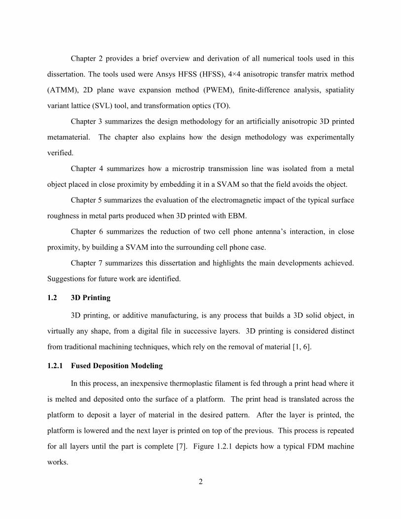
for all layers until the part is complete [7]. Figure 1.2.1 depicts how a typical FDM machine
works.
3
Figure 1.2.1: Illustration of FDM machine [8]
1.2.3 Stereolithography
In this process, a vat of liquid ultraviolet (uv) curable photopolymer, also called resin, is
cured with a low-power, highly focused uv-laser, one layer at a time. Each layer, a cross section
of the part, is exposed to the uv-laser, which causes the resin to solidify. After the layer
solidifies, the platform is then lowered and the process is then repeated until the part is
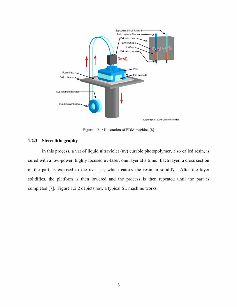
completed [7]. Figure 1.2.2 depicts how a typical SL machine works.
4
Figure 1.2.2: Illustration for SL machine [9]
1.2.4 Electron Beam Melting
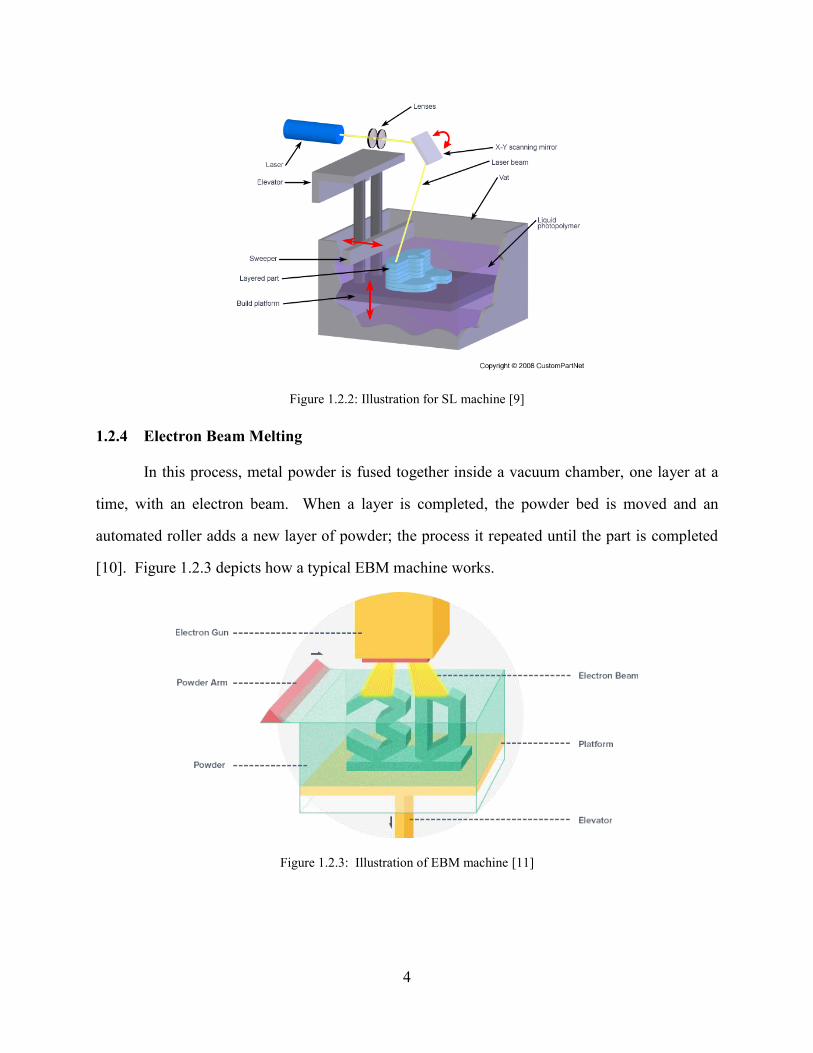
In this process, metal powder is fused together inside a vacuum chamber, one layer at a
time, with an electron beam. When a layer is completed, the powder bed is moved and an
automated roller adds a new layer of powder; the process it repeated until the part is completed
[10]. Figure 1.2.3 depicts how a typical EBM machine works.
Figure 1.2.3: Illustration of EBM machine [11]
5
1.3 Anisotropic Materials
In some materials, charges are more easily displaced along certain directions. For this
reason, the material can become polarized in directions slightly different than the applied field.
In this case, the electric susceptibility, [χe], is a tensor quantity.
0
x xx xy xz x
y yx yy yz y
z zx zy z z
P E
P E
P E
(1.1)
This is most often treated through a dielectric tensor.
1r e (1.2)
The constitutive relation between the electric field, E , and the electric flux density, D , in an
anisotropic medium is
0
x xx xy xz x
y yx yy yz y
z zx zy zz z
D E
D E
D E
(1.3)
Analogously, this can be done for the magnetic flux density, B, using the magnetic susceptibility,
[χm]. This means that the fields are no longer independent of each other [12]. Equation (1.4) is
the magnetic response of a fully anisotropic material.
0
x xx xy xz x
y yx yy yz y
z zx zy zz z
B H
B H
B H
(1.4)
1.4 Electromagnetic Metamaterials
Currently, there is no universally accepted definition for metamaterials. The most basic
definition of a metamaterial is any material that is simply anything other than an ordinary
material [13]. There are recurring themes in literature that describe metamaterials such as:
engineered composites [14], material properties that are derived from their physical structure
6
rather than their chemistry [15], exhibit properties not observed in nature [13], and exhibit
properties not observed in their constituent materials [16]. This dissertation offers the following
definition: “A composite material that is purposely engineered to provide material properties that
are not otherwise attainable with ordinary materials [12].”
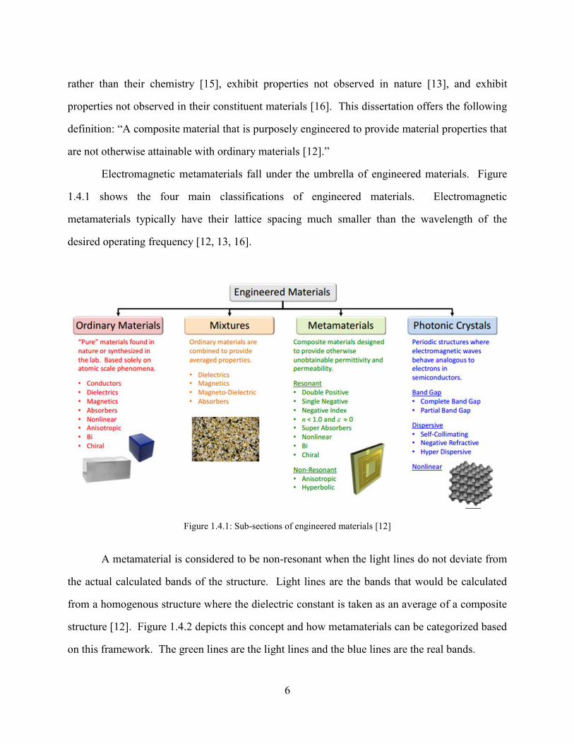
Electromagnetic metamaterials fall under the umbrella of engineered materials. Figure
1.4.1 shows the four main classifications of engineered materials. Electromagnetic
metamaterials typically have their lattice spacing much smaller than the wavelength of the
desired operating frequency [12, 13, 16].
Figure 1.4.1: Sub-sections of engineered materials [12]
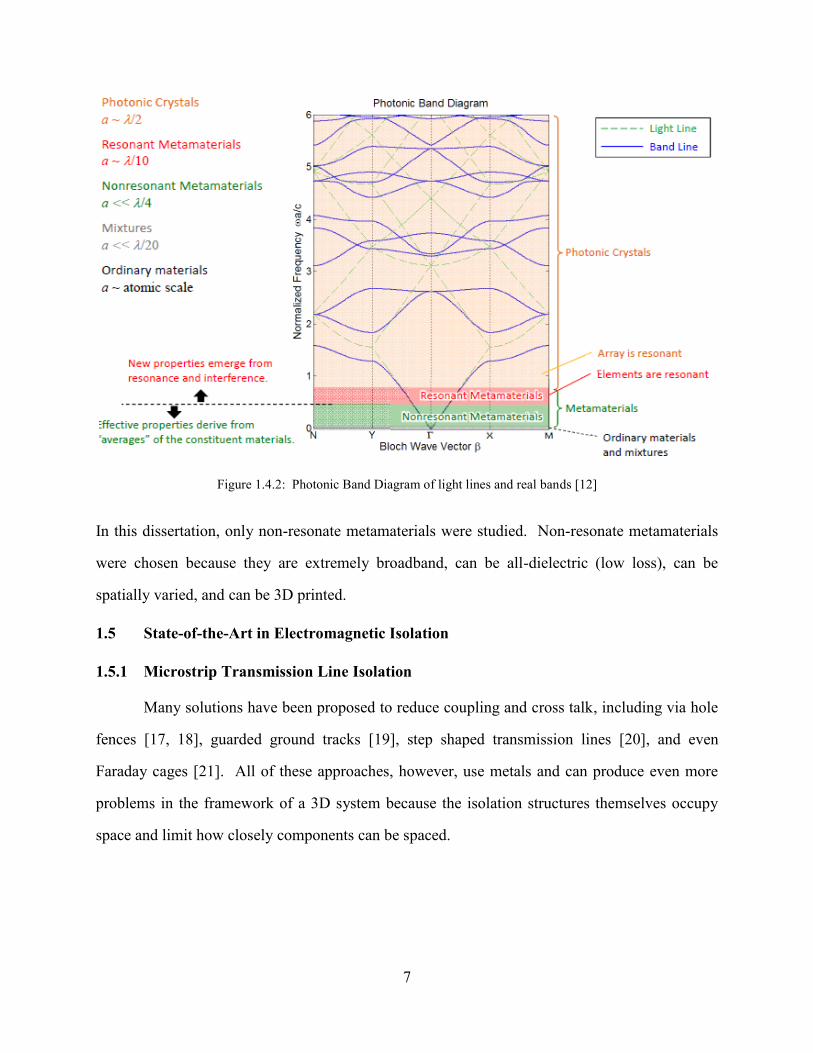
A metamaterial is considered to be non-resonant when the light lines do not deviate from
the actual calculated bands of the structure. Light lines are the bands that would be calculated
from a homogenous structure where the dielectric constant is taken as an average of a composite
structure [12]. Figure 1.4.2 depicts this concept and how metamaterials can be categorized based
on this framework. The green lines are the light lines and the blue lines are the real bands.
7
Figure 1.4.2: Photonic Band Diagram of light lines and real bands [12]
In this dissertation, only non-resonate metamaterials were studied. Non-resonate metamaterials
were chosen because they are extremely broadband, can be all-dielectric (low loss), can be
spatially varied, and can be 3D printed.
1.5 State-of-the-Art in Electromagnetic Isolation
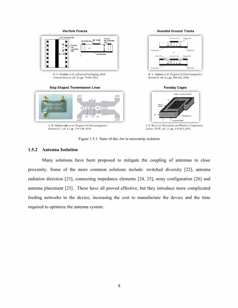
1.5.1 Microstrip Transmission Line Isolation
Many solutions have been proposed to reduce coupling and cross talk, including via hole
fences [17, 18], guarded ground tracks [19], step shaped transmission lines [20], and even
Faraday cages [21]. All of these approaches, however, use metals and can produce even more
problems in the framework of a 3D system because the isolation structures themselves occupy
space and limit how closely components can be spaced.
8
Figure 1.5.1: State-of-the-Art in microstrip isolation
1.5.2 Antenna Isolation
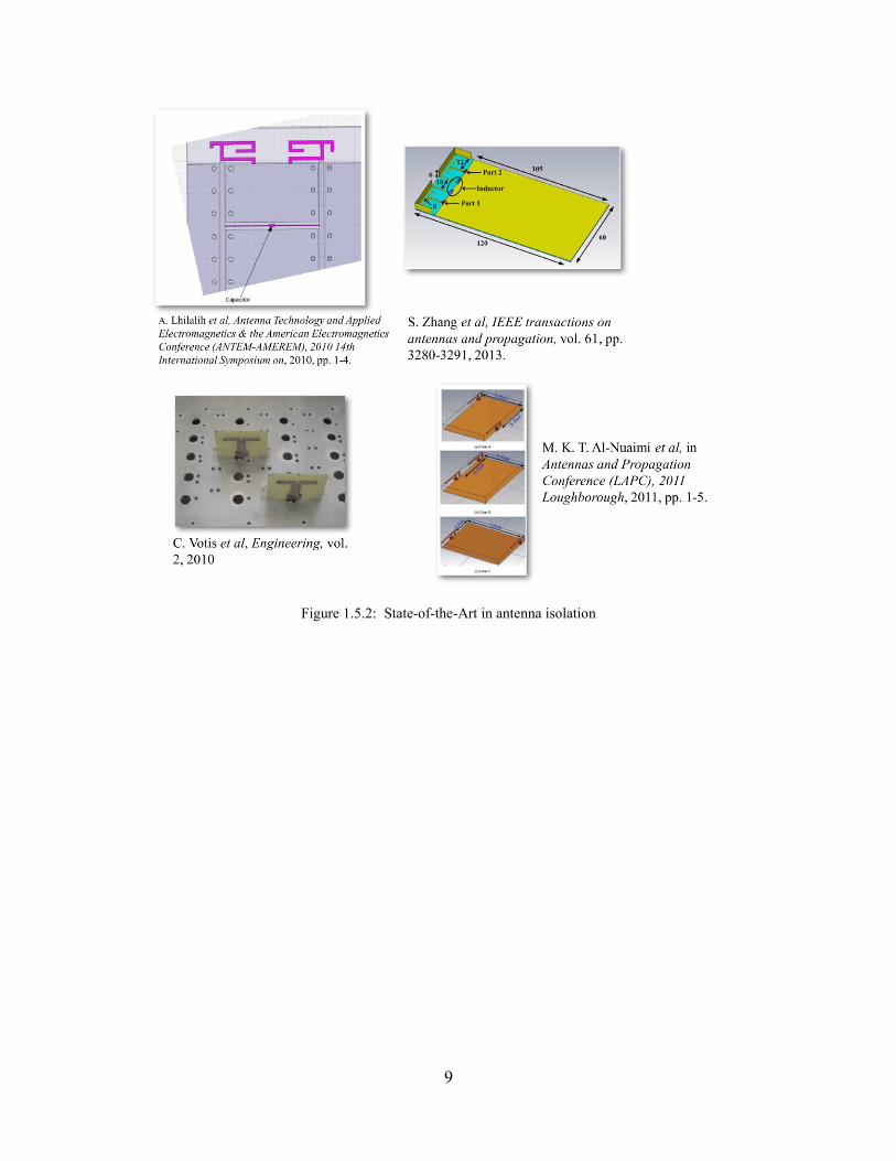
Many solutions have been proposed to mitigate the coupling of antennas in close
proximity. Some of the more common solutions include: switched diversity [22], antenna
radiation direction [23], connecting impedance elements [24, 25], array configuration [26] and
antenna placement [23]. These have all proved effective, but they introduce more complicated
feeding networks to the device, increasing the cost to manufacture the device and the time
required to optimize the antenna system.
9
Figure 1.5.2: State-of-the-Art in antenna isolation

10
Chapter 2: Numerical Tools
2.1 Ansys® HFSS
HFSS is currently the industry standard for simulating 3-D full-wave electromagnetic
fields. HFSS offers multiple solvers based on the finite element method, integral equations, and
hybrid methods. For each method there is an automated solution process; only the geometry,
material properties, and the desired output need to be selected by the user, although much more
control of the solution process is provided if the user wishes to use it. HFSS automatically
generates the mesh and solves for the electromagnetic fields [27].
Since HFSS requires a 3D geometry, it is not the most efficient solver for devices that
can be solved as a 2D or 1D geometry. Also, it only allows materials to be diagonally
anisotropic which makes it inconvenient for materials that must be defined by a full material
tensor. The geometries are limited to ones that can be drawn in a standard CAD program.
Geometries generated with the SVL tool, explained in Section 2.6, cannot currently be imported
into HFSS to be modeled.
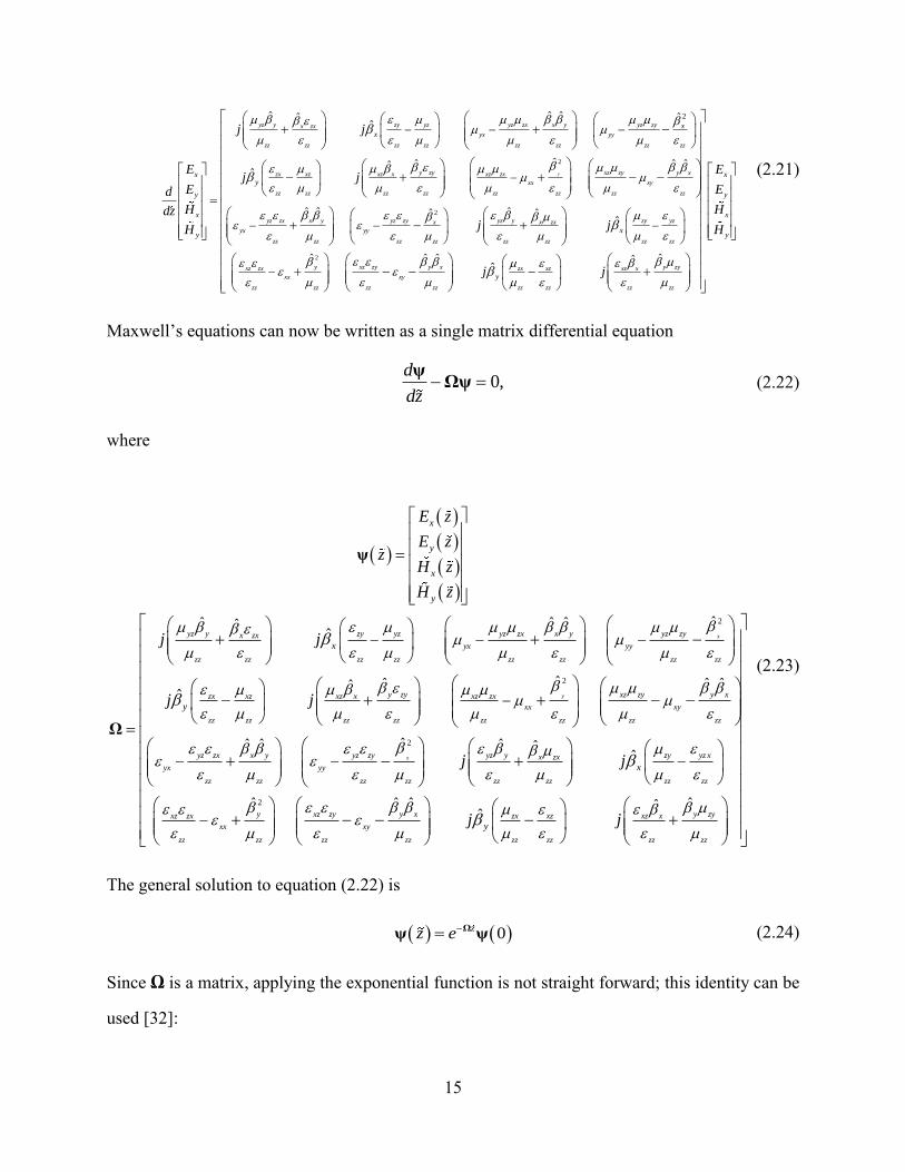
2.2 4 4 Transfer Matrix Method for Anisotropic Materials (ATMM)
ATMM is a very simple, but powerful method, to solve Maxwell’s equations for
anisotropic devices that can be solved as 1D geometries. Each 1D geometry is modeled as a
structure with an infinite cross section and a finite thickness. Those structures can be referred to
as layers. ATMM can account for a large number of layers which are stacked together. Figure
2.2.1 depicts how a 3D problem can be approximated using effective medium approximation, so
ATMM can be used to simulate the device [12, 28].
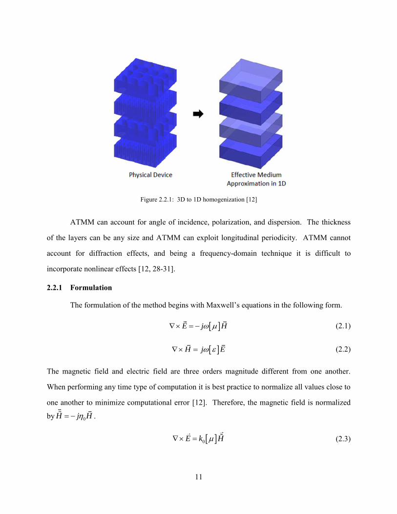
11
Figure 2.2.1: 3D to 1D homogenization [12]
ATMM can account for angle of incidence, polarization, and dispersion. The thickness
of the layers can be any size and ATMM can exploit longitudinal periodicity. ATMM cannot
account for diffraction effects, and being a frequency-domain technique it is difficult to
incorporate nonlinear effects [12, 28-31].
2.2.1 Formulation
The formulation of the method begins with Maxwell’s equations in the following form.
E j H (2.1)
H j E (2.2)
The magnetic field and electric field are three orders magnitude different from one another.
When performing any time type of computation it is best practice to normalize all values close to
one another to minimize computational error [12]. Therefore, the magnetic field is normalized
by 0H j H .
0E k H (2.3)
12
0H k E (2.4)
These vector equations expand to six coupled scalar partial differential equations.
0
0
0
yzxx x xy y xz z
x zyx x yy y yz z
y xzx x zy y zz z
EEk H H H
y z
E Ek H H H
z x
E Ek H H H
x y
(2.5)
0
0
0
yzxx x xy y xz z
x zyx x yy y yz z
y xzx x zy y zz z
HHk E E E
y z
H Hk E E E
z x
H Hk E E E
x y
(2.6)
Waves propagating in a homogeneous layer are a plane wave, and have the following
mathematical form.
0
0
j x j y j z
j x j y j z
E r E e e e
H r H e e e
(2.7)
Taking the derivatives of these solutions, we see that
x xE r j E r jx x
(2.8)
y yE r j E r jy y
(2.9)
Maxwell’s equations then become
13
0
0
0
y
y z xx x xy y xz z
xx z yx x yy y yz z
x y y x zx x zy y zz z
dEj E k H H H
dz
dEj E k H H H
dz
j E j E k H H H
(2.10)
0
0
0
y
y z xx x xy y xz z
xx z yx x yy y yz z
x y y x zx x zy y zz z
dHj H k E E E
dz
dHj H k E E E
dz
j H j H k E E E
(2.11)
Normalizing Maxwell’s equations according to
0
0 0
ˆ ˆz, , yx
x yz kk k
(2.12)
ˆ
ˆ
ˆ ˆ
y
y z xx x xy y xz z
xx z yx x yy y yz z
x y y x zx x zy y zz z
dEj E H H H
dz
dEj E H H H
dz
j E j E H H H
(2.13)
0
0
0
ˆ
ˆ
ˆ ˆ
y
y z xx x xy y xz z
xx z yx x yy y yz z
x y y x zx x zy y zz z
dHj H k E E E
dz
dHj H k E E E
dz
j H j H k E E E
(2.14)
Solving equations (2.13) and (2.14) for the longitudinal components
ˆ
ˆ
ˆ ˆˆ ˆ
y
y z xx x xy y xz z
xx z yx x yy y yz z
y x x y zy yzx xx y y x zx x zy y zz z z
zz zz zz zz
dEj E H H H
dz
dEj E H H H
dz
j E j E HHj E j E H H H H
(2.15)
14
ˆ
ˆ
ˆ ˆˆ ˆ
y
y z xx x xy y xz z
xx z yx x yy y yz z
y x x y zy yzx xx y y x zx x zy y zz z z
zz zz zz zz
dHj H E E E
dz
dHj H E E E
dz
j H j H EEj H j H E E E E
(2.16)
Eliminating the longitudinal components by substitution
2
2
ˆ ˆ ˆ ˆ ˆ ˆ ˆ
ˆˆ ˆ ˆ ˆˆ
y
x
y x y zx y zy y xz y xz zyxz x xz zx
x y x y xx x xy y x y x y
zz zz zz zz zz zz zz zz
x y x zy yzx x zx
x y x y yx x yy y
zz zz zz zz
j j dE j jH H E E H H E E H H
dz
j jdE jH H E E H H
dz
ˆy yz x yz zx yz zy
x y x y
zz zz zz zz
jE E H H
(2.17)
2
2
ˆ ˆ ˆ ˆ ˆ ˆ ˆ
ˆˆ ˆ ˆ ˆˆ
y
x
y x y zx y zy y xz y xz zyxz x xz zx
x y x y xx x xy y x y x y
zz zz zz zz zz zz zz zz
x y x zy yz yx x zx
x y x y yx x yy y
zz zz zz zz z
j j dH j jE E H H E E H H E E
dz
j jdH jE E H H E E
dz
ˆyz x yz zx yz zy
x y x y
z zz zz zz
jH H E E
(2.18)
Rearranging equations(2.17) and (2.18)
2ˆˆ ˆ ˆˆ
ˆˆ
ˆ
ˆ
xyz y zy yz yz zx x y yz zyx x zx
x y yx x yy y
zz zz zz zz zz zz zz zz
y y zyzx xz xz x xz zx
x y xx
zz zz zz zz zz
x
y
dEE E H H
dz
dEE E
dz
j j
j j
2ˆ ˆ ˆy xz zy y x
x xy y
zz zz zz
H H
(2.19)
2
2
ˆˆ ˆ ˆ ˆ
ˆ ˆ ˆ
ˆx
y
yz zx x y yz zy yz y zy yz xx x zx
yx x yy y x y
zz zz zz zz zz zz zz zz
y xz zy y xxz zx
xx x xy y
zz zz zz zz
x
dHE E H H
dz
dHE E
dz
j j
j
ˆ zx xz
x y
zz zz
yH H
(2.20)
Writing equations (2.19) and (2.20) in matrix form
15
2ˆ ˆ ˆˆ ˆ
ˆˆ
ˆ
ˆ
yz y zy yz yz zx x y yz zyx zx
yx yy
zz zz zz zz zz zz zz zz
y zyzx xz xz x xz zx
zz zz zz zz zz
xx
xy
y
x
y
j j
Ej j
Ed
Hdz
H
2
2
2
ˆ ˆ ˆ
ˆ ˆ ˆˆ ˆ
ˆ
ˆ
y xz zy y x
xx xy
zz zz zz
yz zx x y yz zy yz y zy yzx x zx
yx yy
zz zz zz zz zz zz zz zz
y xz zyxz zx
xx xy
zz zz zz
xj j
ˆ ˆ ˆˆˆy x y zyzx xz xz x
zz zz zz zz zz
x
y
x
y
y
E
E
H
H
j j
(2.21)
Maxwell’s equations can now be written as a single matrix differential equation
0,d
dz
ψΩψ (2.22)
where
2ˆˆ ˆ ˆˆ
ˆˆ
ˆ
ˆ
xyz y zy yz yz zx x y yz zyx zx
yx yy
zz zz zz zz zz zz zz zz
y zyzx xz xz x
zz zz zz zz
x
y
x
y
x
y
E z
E zz
H z
H z
j j
j j
ψ
Ω
2
2
2
ˆ ˆ ˆ
ˆˆ ˆ ˆ ˆ
ˆ
ˆ
y
x
xz zy y xxz zx
xx xy
zz zz zz zz
yz zx x y yz zy yz y zy yz xx zx
yx yy
zz zz zz zz zz zz zz zz
yxz zx
xx
zz zz
xj j
ˆ ˆ ˆˆ
ˆxz zy y x y zyzx xz xz x
xy
zz zz zz zz zz zz
yj j
(2.23)
The general solution to equation (2.22) is
0zz e Ωψ ψ (2.24)
Since Ω is a matrix, applying the exponential function is not straight forward; this identity can be
used [32]:
16
1( )f f A W λ W (2.25)
Where A is a matrix, W is the Eigen-vector matrix of A, λ is the Eigen-value matrix of A, and
is the function performed on A. Therefore
1z ze e Ω λW W (2.26)
Equation (2.24) becomes
1 0zz e λψ W W ψ (2.27)
Equation (2.27) can be rewritten as
1; where 0zz e λψ W c c W ψ (2.28)
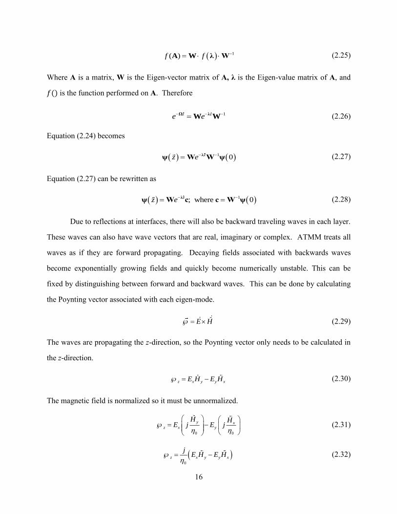
Due to reflections at interfaces, there will also be backward traveling waves in each layer.
These waves can also have wave vectors that are real, imaginary or complex. ATMM treats all
waves as if they are forward propagating. Decaying fields associated with backwards waves
become exponentially growing fields and quickly become numerically unstable. This can be
fixed by distinguishing between forward and backward waves. This can be done by calculating
the Poynting vector associated with each eigen-mode.
E H (2.29)
The waves are propagating the z-direction, so the Poynting vector only needs to be calculated in
the z-direction.
z x y y xE H E H (2.30)
The magnetic field is normalized so it must be unnormalized.
0 0
y xz x y
H HE j E j
(2.31)
0
z x y y x
jE H E H
(2.32)
17
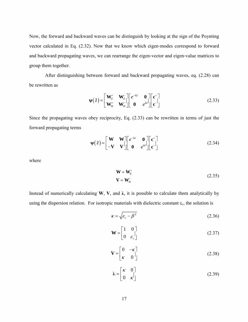
Now, the forward and backward waves can be distinguish by looking at the sign of the Poynting
vector calculated in Eq. (2.32). Now that we know which eigen‐modes correspond to forward
and backward propagating waves, we can rearrange the eigen‐vector and eigen‐value matrices to
group them together.
After distinguishing between forward and backward propagating waves, eq. (2.28) can
be rewritten as
z
E E
z
H H
ez
e
λ
λ
W W 0 cψ
W W 0 c (2.33)
Since the propagating waves obey reciprocity, Eq. (2.33) can be rewritten in terms of just the
forward propagating terms
z
z
ez
e
λ
λ
W W 0 cψ
V V 0 c (2.34)
where
E
H
W W
V W (2.35)
Instead of numerically calculating W, V, and λ, it is possible to calculate them analytically by
using the dispersion relation. For isotropic materials with dielectric constant εc, the solution is
2
c (2.36)
1 0
0 c
W (2.37)
0
0
V (2.38)
0
0
λ (2.39)
18
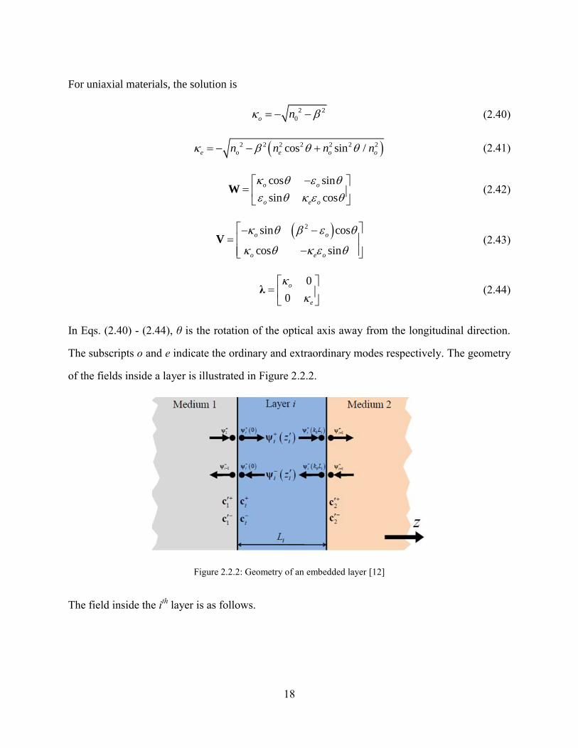
For uniaxial materials, the solution is
2 2
0o n (2.40)
2 2 2 2 2 2 2cos sin /e o e o on n n n (2.41)
cos sin
sin cos
o o
o e o
W (2.42)
2sin cos
cos sin
o o
o e o
V (2.43)
0
0
o
e
λ (2.44)
In Eqs. (2.40) - (2.44), θ is the rotation of the optical axis away from the longitudinal direction.
The subscripts o and e indicate the ordinary and extraordinary modes respectively. The geometry
of the fields inside a layer is illustrated in Figure 2.2.2.
Figure 2.2.2: Geometry of an embedded layer [12]
The field inside the ith
layer is as follows.
19
,
,
,
,
( )
( ) 0(z)=
( ) 0
( )
i
i
x i
zy i i i i
zx i i i i
y i
E z
E z e
H z e
H z
λ
λ
W W cψ
V V c (2.45)
The boundary conditions at the first interface are as follows.
1
1 1 1
1 1 1
(0)i
i i i
i i i
ψ ψ
W WW W cc
V VV -V cc
(2.46)
The boundary conditions at the second interface are as follows.
0
0
0 2
2 2 2
2 2 2
i
i
i i
k Li i i
k Li i i
k L
e
e
λ
λ
ψ ψ
W W W Wc c0
V V V Vc c0
(2.47)
The scattering matrix Si of the ith
layer is defined as
1 1 11 12
2 2 21 22
i i
i i i i
c c S SS S
c c S S (2.48)
After some algebra, which is shown in appendix A1, the components of the transfer matrix are
computed as
0
1 1
,
1 1
,
i i
i j i j i j
i j i j i j
k L
i e
λ
A W W V V
B W W V V
X
(2.49)
11 1
11 , 1 , 1 , 1 , 1 , 1 , 1 , 1 , 1
11 1
12 , 1 , 1 , 1 , 1 , 1 , 1 , 1 , 1
11 1
21 , 1 , 1 , 1 , 1 , 1 , 1 , 1 ,
i
i i i i i i i i i i i i i i i i i i i i
i
i i i i i i i i i i i i i i i i i i i
i
i i i i i i i i i i i i i i i i i i
s A X B A X B X B A X A B
s A X B A X B X A B A B
s A X B A X B X A B A B
1
11 1
22 , 1 , 1 , 1 , 1 , 1 , 1 , 1 , 1
i
i
i i i i i i i i i i i i i i i i i i i i
s A X B A X B X B A X A B
(2.50)
The transfer matrix method consists of working through the device one layer at a time and
calculating an overall (global) scattering matrix.
20
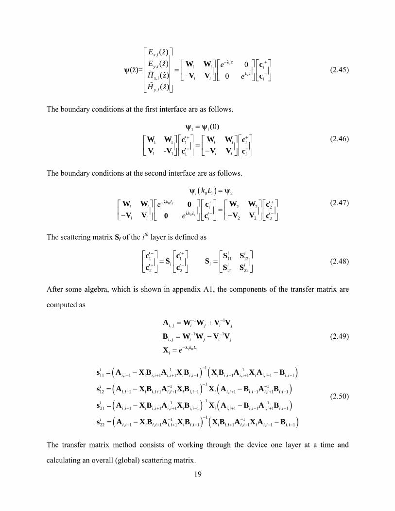
global 5 4 3 2 1 S S S S S S (2.51)
Here the operator denotes the Redheffer star product [33]. The definition of the Redheffer
star product is as follows.
11 12 11 12
21 22 21 22
b a b a
b b a aS S S S S
b b a a (2.52)
The combined scattering matrix is then
11 12
21 22
1
11 11 12 11 22 11 21
1
12 12 11 22 12
1
21 21 22 11 21
1
22 11 21 22 11 22 12
( )
( )
( )
( )
S SS
S S
S a a I b a b a
S a I b a b
S b I a b a
S b b I a b a b
(2.53)
The final scattering matrix is
11 121 1
21 222 2
S Sc c
S Sc c (2.54)
2.3 2D Plane Wave Expansion Method
The PWEM is extremely efficient for calculating the band diagrams for periodic
structures. PWEM works best with unit cells that are on the order of a wavelength and have a
low to moderate refractive index contrast [34-39].
2.3.1 Formulation
The method begins with Maxwell’s equations in the following form
0 rE j H (2.55)
0 rH j Ea (2.56)
After normalizing the magnetic field according to 0H j H , Maxwell’s equations become
21
0 rE k H (2.57)
0 rH k E (2.58)
These vector equations expand into six coupled scalar partial differential equations.
0
0
0
yzr x
x zr y
y xr z
EEk H
y z
E Ek H
z x
E Ek H
x y
(2.59)
0
0
0
yzr x
x zr y
y xr z
HHk E
y z
H Hk E
z x
H Hk E
x y
(2.60)
These equations can be Fourier transformed, shown in detail in [40], which yields:
, , , , 0 ,
, , , , 0 ,
, , , , 0 ,
y pqr z pqr z pqr y pqr pqr x pqr
z pqr x pqr x pqr z pqr pqr y pqr
x pqr y pqr y pqr x pqr pqr z pqr
k S k S jk U
k S k S jk U
k S k S jk U
(2.61)
, , , , 0 ,
, , , , 0 ,
, , , , 0 ,
y pqr z pqr z pqr y pqr pqr x pqr
z pqr x pqr x pqr z pqr pqr y pqr
x pqr y pqr y pqr x pqr pqr z pqr
k U k U jk S
k U k U jk S
k U k U jk S
(2.62)
Each of these equations is written once for every spatial harmonic (Fourier term) retained
in the expansion. This large set of equations can be written in matrix form as
0y z z y r xjk K s K s μ u (2.63)
0z x x z r yjk K s K s μ u (2.64)
22
0x y y x r zjk K s K s μ u (2.65)
0y z z y r xjk K u K u ε s (2.66)
0z x x z r yjk K u K u ε s (2.67)
0x y y x r zjk K u K u ε s (2.68)
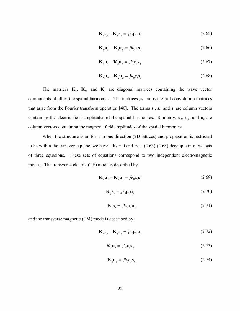
The matrices Kx. Ky, and Kz are diagonal matrices containing the wave vector
components of all of the spatial harmonics. The matrices μr and εr are full convolution matrices
that arise from the Fourier transform operation [40]. The terms sx, sy, and sz are column vectors
containing the electric field amplitudes of the spatial harmonics. Similarly, ux, uy, and uz are
column vectors containing the magnetic field amplitudes of the spatial harmonics.
When the structure is uniform in one direction (2D lattices) and propagation is restricted
to be within the transverse plane, we have Kz = 0 and Eqs. (2.63)-(2.68) decouple into two sets
of three equations. These sets of equations correspond to two independent electromagnetic
modes. The transverse electric (TE) mode is described by
0x y y x r zjk K u K u ε s (2.69)
0y z r xjkK s μ u (2.70)
0x z r yjk K s μ u (2.71)
and the transverse magnetic (TM) mode is described by
0x y y x r zjk K s K s μ u (2.72)
0y z r xjkK u ε s (2.73)
0x z r yjk K u ε s (2.74)
23
A matrix wave equation can be derived for each of the above modes just in terms of either sz or
uz. These are
1 1 2
0 TE Modex r x y r y z r zk K μ K K μ K s ε s (2.75)
1 1 2
0 TM Modex r x y r y z r zk K ε K K ε K u μ u (2.76)
These can be recognized as generalized eigen-value problems where 2
0k is the eigen-value. The
E mode has the electric field polarized out of the transverse plane while the H mode has the
electric field polarized within the transverse plane.
2.4 Finite-Difference Analysis of Arbitrary Transmission Lines Embedded in
Anisotropic Media
The fundamental mode in a transmission line is very close to TEM (transverse
electromagnetic) mode. In this case, the analysis reduces to an electrostatic problem and
transmission lines can be modeled using the inhomogeneous Laplace’s equation instead of the
more rigorous wave equation. This is done for greater speed and efficiency.
2.4.1 Formulation
Starting with Maxwell’s divergence equation, the constitutive relation for the electric
field in an anisotropic material, and the relation between the electric field and the scalar potential
is given by
,0
,
x
y
D x y
D x yx y
(2.77)
0
, , , ,
, , , ,
x xx xy x
y yx yy y
D x y x y x y E x y
D x y x y x y E x y
(2.78)
,,
,
x
y
E x y xV x y
E x y y
(2.79)

24
Deriving the inhomogeneous Laplace’s equation by substituting Eq. (2.78) into (2.77) to
eliminate the D field, and then substituting Eq. (2.79) into this new expression to eliminate the E
field we obtain
, ,, 0
, ,
xx xy
yx yy
x y x y xV x y
x y x y yx y
(2.80)
Given a solution to this equation, the E field can be computed using (2.79) and then the D field
computed using Eq. (2.78). At this point, all of the fields surrounding the device are known, can
be visualized, and can be used to calculate the transmission line parameters. First, we calculate
the distributed capacitance C of the line by looking it at as a capacitor. Given the electric fields,
the total energy U stored in this system is
1
2A
U D E dxdy (2.81)
This integral is taken over the entire cross section of the transmission line and must encompass
all of the field energy. The energy stored in a capacitor is related to its capacitance C and stored
voltage V0 through Eq. (2.82).
2
0 2U CV (2.82)
Combining Eqs. (2.81) and (2.82) gives an equation to calculate the distributed capacitance from
the electric fields.
2
0
1
A
C D E dxdyV
(2.83)
Second, if the medium surrounding the transmission line has no magnetic response, we can
calculate the distributed inductance L directly from the distributed capacitance Cair of the same
transmission line embedded in air instead of the anisotropic dielectric. In this case, the velocity
of the wave on the line is related to the transmission line parameters through 0
1air
c LC .
Solving this for L yields
25
2
01 .airL c C (2.84)
Given the distributed inductance and capacitance, the characteristic impedance of the
transmission line is
0Z L C (2.85)
and the propagation constant at frequency ω is
.LC (2.86)
2.4.2 Numerical Solution to Equation (2.80)
The remaining challenge is to obtain the solution to Eq. (2.80). This was solved using a
simple finite-difference method. This approach approximates the derivatives using central finite-
differences. To handle this in a straightforward manner, we staggered the position of Ex, Ey, and
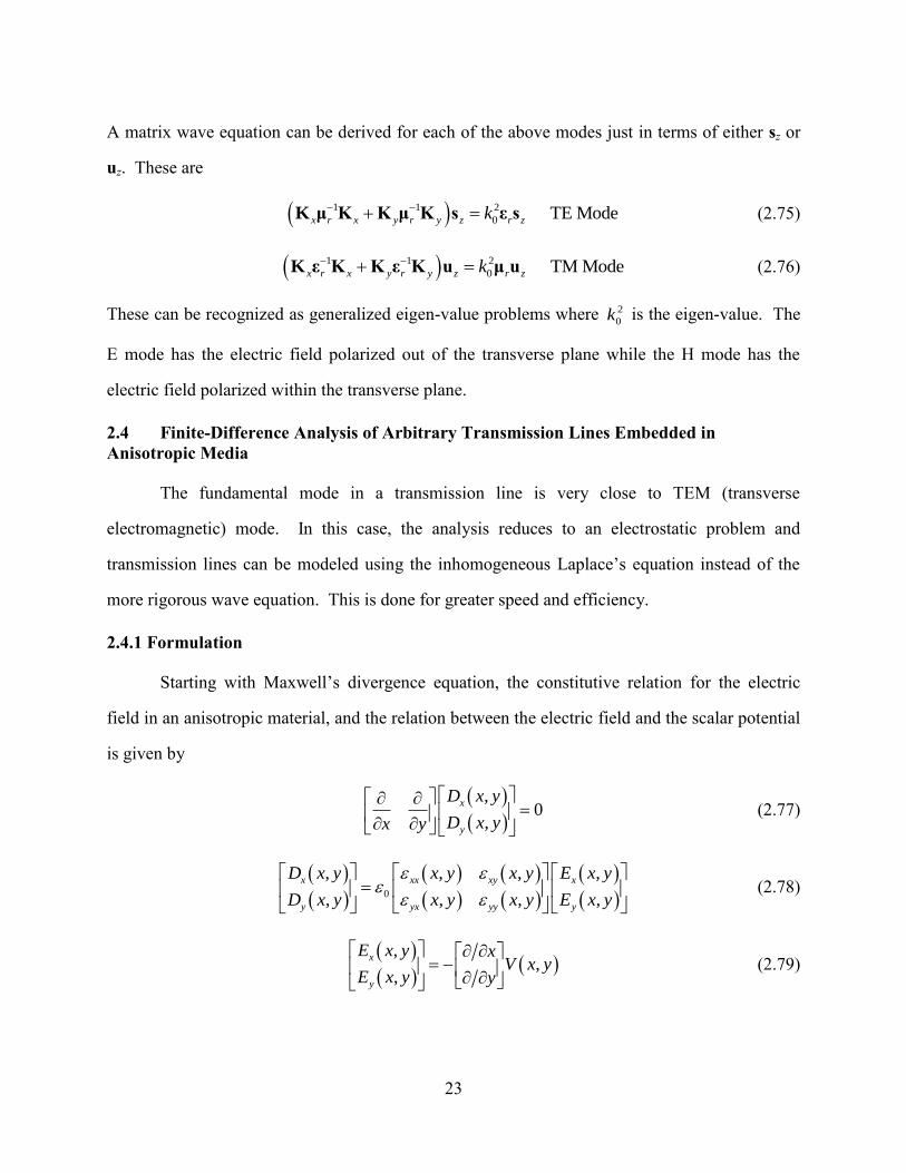
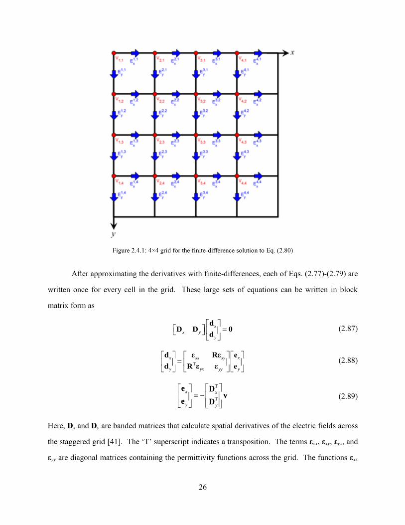
V across a two-dimensional (2D) grid. The position of these terms across a 4×4 grid is illustrated
in Figure 2.4.1. The potential is located at the origin of each cell in the grid. The electric fields
are positioned at the cell boundaries, but offset from the origin by a half cell.
26
Figure 2.4.1: 4×4 grid for the finite-difference solution to Eq. (2.80)
After approximating the derivatives with finite-differences, each of Eqs. (2.77)-(2.79) are
written once for every cell in the grid. These large sets of equations can be written in block
matrix form as
x
x y
y
dD D 0
d (2.87)
T
x xx xy x
y yx yy y
d ε Rε e
d R ε ε e (2.88)
T
T
x x
y y
e Dv
e D (2.89)
Here, Dx and Dy are banded matrices that calculate spatial derivatives of the electric fields across
the staggered grid [41]. The ‘T’ superscript indicates a transposition. The terms εxx, εxy, εyx, and
εyy are diagonal matrices containing the permittivity functions across the grid. The functions εxx
27
and εyx are defined to be at the same points as Ex while the functions εxy and εyy are defined at the
same points as Ey. R is a banded matrix that interpolates the Ey quantities to be at the same
positions as the Ex quantities [41]. RT is the transpose of R and interpolates Ex quantities to be at
the same positions as the Ey quantities. The terms dx, dy, ex and ey are column vectors containing
the field components Dx, Dy, Ex, and Ey respectively throughout the grid. Lastly, v is a column
vector containing the scalar potential V throughout the grid. The matrix form of Eq. (2.80) is
derived by substituting Eq. (2.88) into Eq. (2.87) to eliminate dx and dy, and then using Eq.
(2.89) to eliminate ex and ey. The resulting block equation can be written as
Lv 0 (2.90)
T
T.
xx xy x
Tx y
yx yy y
ε Rε DL D D
R ε ε D (2.91)
Eq. (2.90) has only a trivial solution because we have not yet defined the potential applied to the
conductors. To do this, we construct a diagonal matrix F which has 1’s in the diagonal positions
corresponding to where conductors are placed on the grid. 0’s are placed everywhere else. We
further construct a column vector vf which contains the voltages applied to each of the
conductors identified in F. Given these, we modify (2.90) according to [41]
L v b (2.92)
L F I F L (2.93)
.fb Fv (2.94)
We can now numerically solve Eq. (2.92) as 1v L b . Given v, the E field
components are calculated using Eq. (2.89) and then the D field components are calculated using
Eq. (2.88). After these functions are obtained, the distributed capacitance is calculated according
to Eq. (2.95).
28
0
2
0
.x
x y
y
x yC
V
ed d
e (2.95)
Note that the free space permittivity ε0 was removed from Eq. (2.88) and inserted here for
convenience. The entire solution process is repeated with the dielectric set to air. In this case,
Eq. (2.91) reduces to the homogeneous Laplace’s equation.
T
T
x
h x y
y
DL D D
D (2.96)
From this, the distributed inductance L is calculated from the distributed capacitance Cair using
Eq. (2.84). Finally, the characteristic impedance and propagation constant are calculated using
Eq. (2.85) and Eq. (2.86) respectively.
2.4.3 Benchmark Simulations
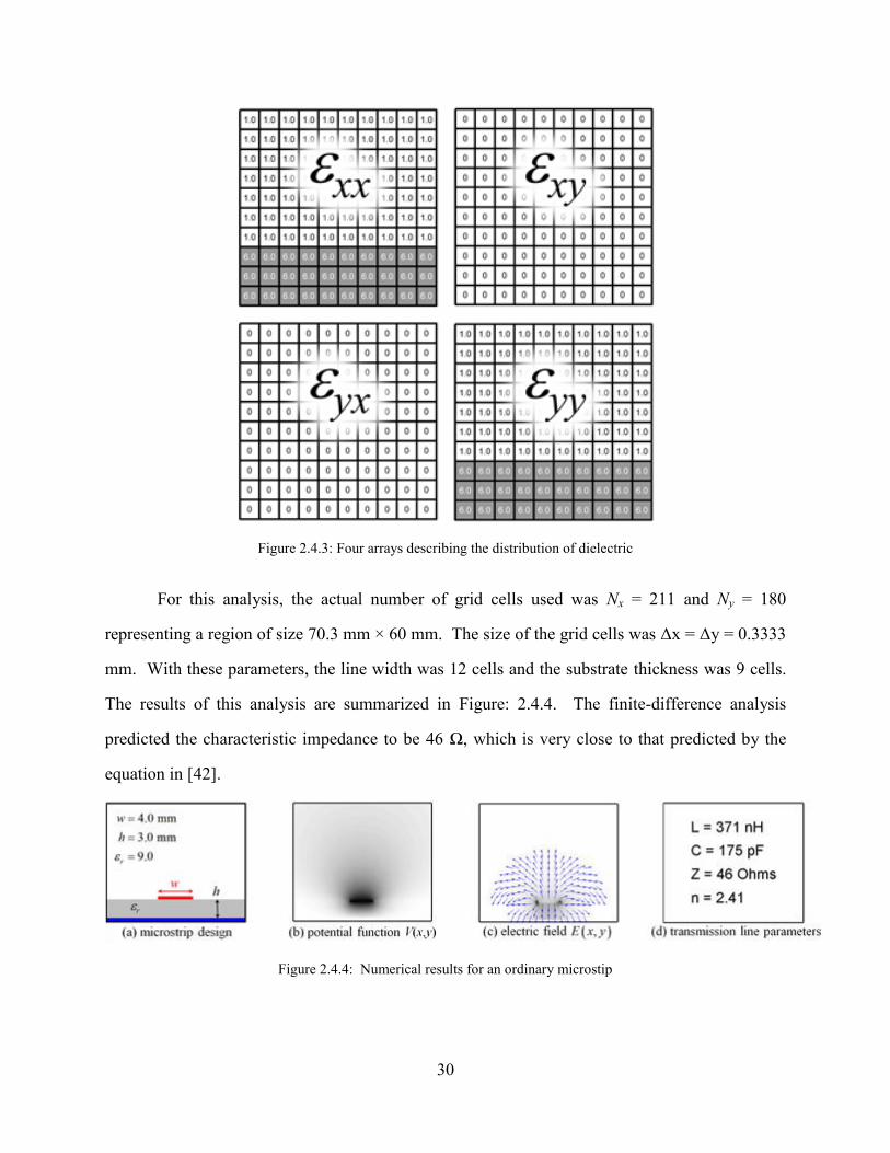
To demonstrate and benchmark the method described above, an ordinary microstrip
transmission line was analyzed. The baseline design was obtained from the closed form
expression in [42]. The width of the microstrip was w = 4.0 mm, the thickness of the substrate
was h = 3.0 mm, and the dielectric constant of the substrate was εr = 9.0. The impedance
calculated analytically using these dimensions was 49 Ω.
The grid strategy for the numerical analysis is illustrated in Figure 2.4.2. In practice,
many more grid cells are needed. The grid cells representing the substrate are shown in gray
while the cells in air are shown in white. In Figure 2.4.2 the grid cells corresponding to the
signal trace are shown in red. The digit ‘1’ in these cells indicates that the potential is forced to
V0 = 1.0 V at these points. The grid cells corresponding to the ground metals are shown in blue.
The digit ‘0’ in these cells indicates that the potential is forced to 0 V at these points. The entire
outer boundary was set to ground as the boundary condition. As long as the spacer regions
shown in green are made large enough, usually 3 to 5 line widths, the model converges to the
properties of a real microstrip in open air.
29
Figure 2.4.2: Grid strategy for finite-difference analysis of a microstrip transmission line
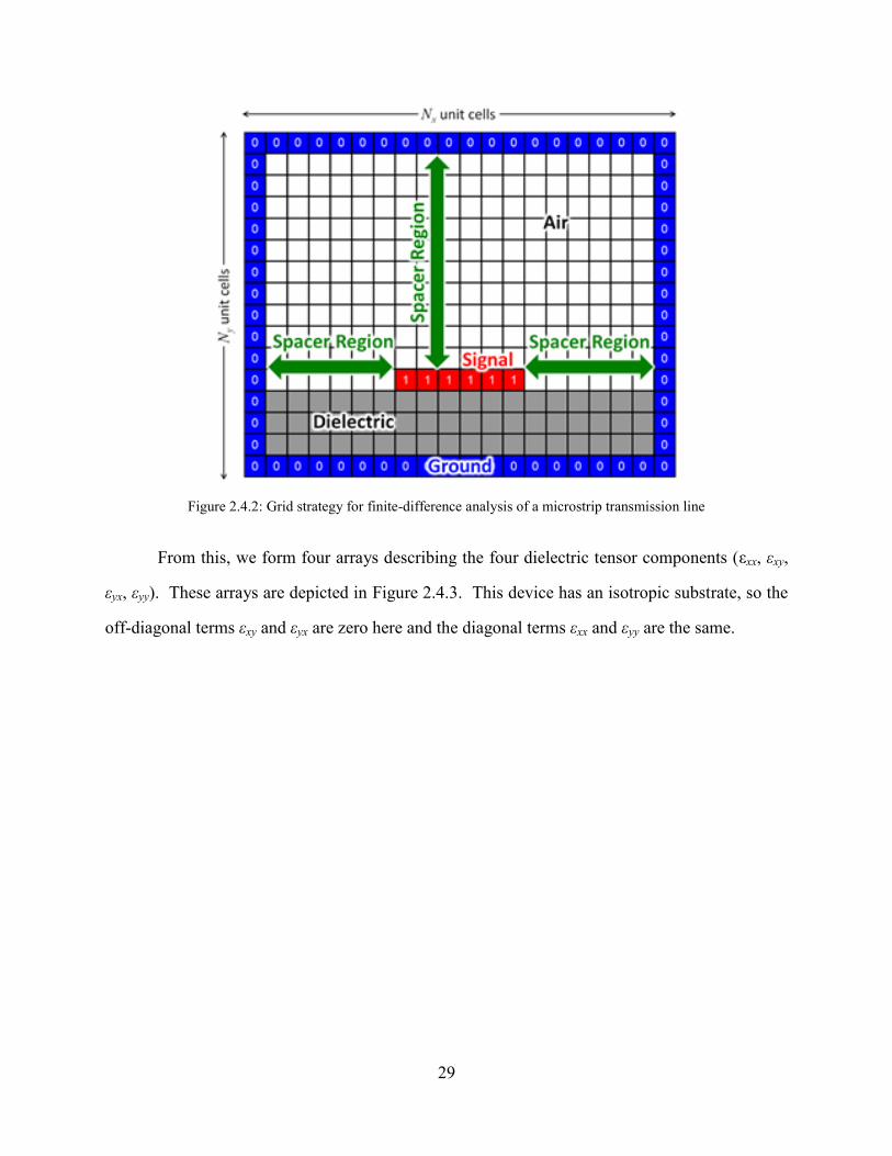
From this, we form four arrays describing the four dielectric tensor components (εxx, εxy,
εyx, εyy). These arrays are depicted in Figure 2.4.3. This device has an isotropic substrate, so the
off-diagonal terms εxy and εyx are zero here and the diagonal terms εxx and εyy are the same.
30
Figure 2.4.3: Four arrays describing the distribution of dielectric
For this analysis, the actual number of grid cells used was Nx = 211 and Ny = 180
representing a region of size 70.3 mm × 60 mm. The size of the grid cells was Δx = Δy = 0.3333
mm. With these parameters, the line width was 12 cells and the substrate thickness was 9 cells.
The results of this analysis are summarized in Figure: 2.4.4. The finite-difference analysis
predicted the characteristic impedance to be 46 Ω, which is very close to that predicted by the
equation in [42].
Figure 2.4.4: Numerical results for an ordinary microstip
31
2.5 Anisotropic Finite-Difference Frequency-Domain Method
This section discusses in detail how the three-dimensional (3D) FDFD method described
in [43] can be modified to incorporate anisotropic materials with arbitrary tensors.
2.5.1 Formulation
The formulation and implementation of the basic FDFD method is described in detail in
[43], but this paper used only diagonal material tensors [μ] and [ε]. Below we generalized the
formulation to incorporate arbitrary material tensors. After normalizing the magnetic field
according to 0H j H , Maxwell’s curl equations with a uniaxial PML (UPML) [44] can be
written as
0 rE k s H (2.97)
0 rH k s E (2.98)
For a UPML, the tensor [s] is expressed as
0 0
0 0
0 0
y z
x
x z
y
x y
z
s s
s
s ss
s
s s
s
(2.99)
Without any approximation to the material tensors, Eqs. (2.97) and (2.98) can be expanded into
the following set of six coupled partial differential equations. The μij and εij terms are relative to
free space because the free space constants μo and εo have already been factored out.
y y zz
xx x xy y xz z
x
E s sEH H H
y z s
(2.100)
x z x zyx x yy y yx z
y
E E s sH H H
z x s
(2.101)
32
y x yx
zx x zy y zz z
z
E s sEH H H
x y s
(2.102)
y y zzxx x xy y zx z
x
H s sHE E E
y z s
(2.103)
x x x zyx x yy y yz z
y
H H s sE E E
z x s
(2.104)
y x yxzx x zy y zz z
z
H s sHE E E
x y s
(2.105)
Here, the grid coordinates have been normalized according to
0 0 0 x k x y k y z k z (2.106)
2.5.1.1 Finite-Difference Approximation of Maxwell’s Equations
Following the procedure outlined in [43], the fields and materials are assigned to discrete
points on a Yee grid [45] and the derivatives in Eqs. (2.100)-(2.105) are approximated using
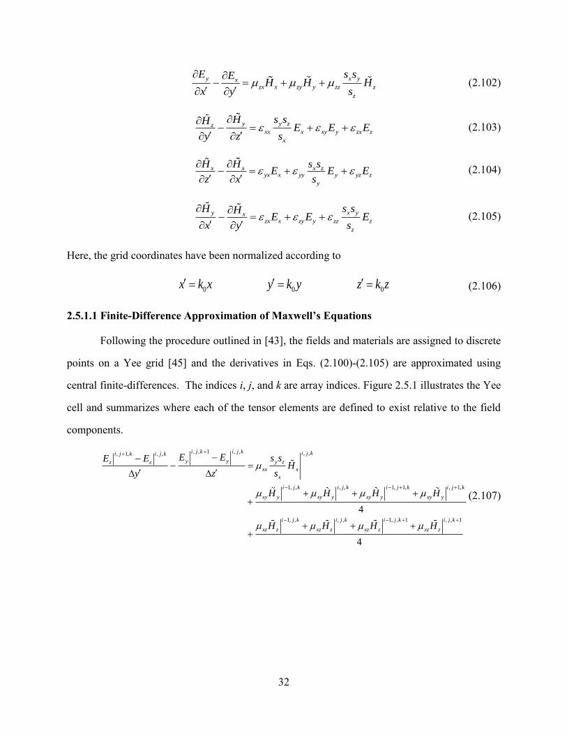
central finite-differences. The indices i, j, and k are array indices. Figure 2.5.1 illustrates the Yee
cell and summarizes where each of the tensor elements are defined to exist relative to the field
components.
, , 1 , , , ,, 1, , ,
1, , , , 1, 1, , 1,
4
i j k i j k i j ki j k i j k
y y y zz z
xx x
x
i j k i j k i j k i j k
xy y xy y xy y xy y
E E s sE EH
y z s
H H H H
1, , , , 1, , 1 , , 1
4
i j k i j k i j k i j k
xz z xz z xz z xz zH H H H
(2.107)
33
, , 1, , , 1, 1, 1,, , 1 , , 1, , , ,
, ,
4
i j k i j k i j k i j ki j k i j k i j k i j k
yx x yx x yx x yx xx x z z
i j k
x zyy y
y
H H H HE E E E
z x
s sH
s
, 1, , , , 1, 1 , , 1
4
i j k i j k i j k i j k
yz z yz z yz z yz zH H H H
(2.108)
, , 1, , , , 1 1, , 11, , , , , 1, , ,
, , , 1, , , 1
4
i j k i j k i j k i j ki j k i j k i j k i j k
zx x zx x zx x zx xy y x x
i j k i j k i j k
zy y zy y zy y zy
H H H HE E E E
x y
H H H
, 1, 1
, ,
4
i j k
y
i j k
x y
zz z
z
H
s sH
s
(2.109)
, , , 1, , , , , 1 , ,
, 1, , , 1, 1, 1, ,
4
i j k i j k i j k i j k i j k
z z y y y z
xx x
x
i j k i j k i j k i j k
xy y xy y xy y xy y
H H H H s sE
y z s
E E E E
, , 1, , , , 1 1, , 1
4
i j k i j k i j k i j k
xz z xz z xz z xz zE E E E
(2.110)
, , , , 1 , , 1, , 1, , , , 1, 1, , 1,
, ,
4
i j k i j k i j k i j k i j k i j k i j k i j k
x x z z yx x yx x yx x yx x
i j k
x zyy y
y
H H H H E E E E
z x
s sE
s
, , , 1, , , 1 , 1, 1
4
i j k i j k i j k i j k
yz z yz z yz z yz zE E E E
(2.111)
, , 1, , , , , 1, 1, , , , 1, , 1 , , 1
, 1, , , , 1, 1
4
i j k i j k i j k i j k i j k i j k i j k i j k
y y x x zx x zx x zx x zx x
i j k i j k i j k
zy y zy y zy y z
H H H H E E E E
x y
E E E
, , 1
, ,
4
i j k
y y
i j k
x y
zz z
z
E
s sE
s
(2.112)
34
In these equations, the terms containing off diagonal tensor elements require special
treatment. Each term in a finite-difference equation must exist at the same point in space. In Eq.
(2.107), each term is defined to exist at the same point as xH . The central finite-difference
ensures that the derivative terms on the left exist at this point. The last two terms on the right
side of this equation are averaged at four points in the grid to interpolate the value at the same
point as xH . The same interpolation operation is used on every term in Eqs. (2.107)-(2.112)
containing an off diagonal element.
Figure 2.5.1 3D Yee cell along with position of the tensor elements
2.5.1.2 Maxwell’s Equations in Matrix Form
Each equation above is written once for every cell in the grid so each finite-difference
equation produces a large set of linear algebraic equations that can be written in matrix form as
e e
y z z y xx x xy y xz z D e D e μ h μ h μ h (2.113)
e e
z x x z yx x yy y yz z D e D e μ h μ h μ h (2.114)
e e
x y y x zx x zy y zz z D e D e μ h μ h μ h (2.115)
h h
y z z y xx x xy y xz z D h D h ε e ε e ε e (2.116)
h h
z x x z yx x yy y yz z D h D h ε e ε e ε e (2.117)
35
h h
x y y x zx x zy y zz z D h D h ε e ε e ε e (2.118)
The terms xe , ye , ze , xh , yh , and zh are column vectors that contain all of the field components
throughout the entire grid reshaped into linear arrays. The terms e
xD , e
yD , and e
zD are banded
matrices that calculate first-order spatial derivatives of the electric fields across the grid.
Similarly, the termsh
xD ,h
yD , and h
zD calculate first-order spatial derivatives of the magnetic
fields across the grid.
When the 3D code is being used to model 2D or 1D systems, the derivatives along the
uniform directions take the special forms in Eq. (2.119) where the wave vector of the source is
given by incˆ ˆ ˆ
x y zk k x k y k z .
0
for devices uniform along , 1e h xx x x
kj x Nk
D D I (2.119)
0
for devices uniform along , 1ye h
y y y
kj y Nk
D D I (2.119)
0
for devices uniform along , 1e h zz z z
kj z Nk
D D I (2.119)
Finally, the terms mnμ and mn
ε are diagonal matrices containing the relative
permeability and relative permittivity of those tensor elements through the grid along their
diagonals. In addition, the PML terms and interpolation operations have been absorbed into
these quantities giving them the following general form. The prime denotes that the material
tensors have been modified.
1
1
1
xx xy xz xx x y z x y xy x z xz
r yx yy yz y x yx yy x y z y z yz
zx zy zz z x zx z y zy zz x y z
μ μ μ μ s s s R R μ R R μ
μ μ μ μ R R μ μ s s s R R μ
μ μ μ R R μ R R μ μ s s s
(2.120)
1
1
1
xx xy xz xx x y z x y xy x z xz
r yx yy yz y x yx yy x y z y z yz
zx zy zz z x zx z y zy zz x y z
ε ε ε ε s s s R R ε R R ε
ε ε ε ε R R ε ε s s s R R ε
ε ε ε R R ε R R ε ε s s s
(2.121)
36
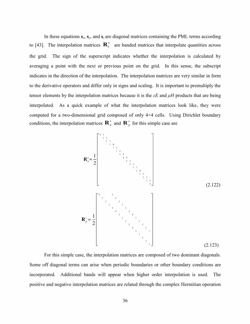
In these equations sx, sy, and sz are diagonal matrices containing the PML terms according
to [43]. The interpolation matrices i
R are banded matrices that interpolate quantities across
the grid. The sign of the superscript indicates whether the interpolation is calculated by
averaging a point with the next or previous point on the grid. In this sense, the subscript
indicates in the direction of the interpolation. The interpolation matrices are very similar in form
to the derivative operators and differ only in signs and scaling. It is important to premultiply the
tensor elements by the interpolation matrices because it is the εE and μH products that are being
interpolated. As a quick example of what the interpolation matrices look like, they were
computed for a two-dimensional grid composed of only 4×4 cells. Using Dirichlet boundary
conditions, the interpolation matrices x
R and y
R for this simple case are
(2.122)
(2.123)
For this simple case, the interpolation matrices are composed of two dominant diagonals.
Some off diagonal terms can arise when periodic boundaries or other boundary conditions are
incorporated. Additional bands will appear when higher order interpolation is used. The
positive and negative interpolation matrices are related through the complex Hermitian operation
37
as H
i i
R R . Using interpolation matrices in this manner allows straightforward
implementation of higher order interpolation schemes without having to modify the rest of the
FDFD code.
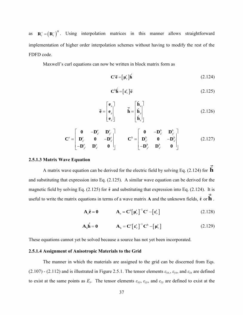
Maxwell’s curl equations can now be written in block matrix form as
e
rC e μ h (2.124)
h
rC h ε e (2.125)
x x
y y
z z
e h
e e h h
e h
(2.126)
e e h h
z y z y
e e e h h h
z x z x
e e h h
y x y x
0 D D 0 D D
C D 0 D C D 0 D
D D 0 D D 0
(2.127)
2.5.1.3 Matrix Wave Equation
A matrix wave equation can be derived for the electric field by solving Eq. (2.124) for h
and substituting that expression into Eq. (2.125). A similar wave equation can be derived for the
magnetic field by solving Eq. (2.125) for e and substituting that expression into Eq. (2.124). It is
useful to write the matrix equations in terms of a wave matrix A and the unknown fields, e or h .
1
h e
e e r r
A e 0 A C μ C ε (2.128)
1
e h
h h r r
A h 0 A C ε C μ (2.129)
These equations cannot yet be solved because a source has not yet been incorporated.
2.5.1.4 Assignment of Anisotropic Materials to the Grid
The manner in which the materials are assigned to the grid can be discerned from Eqs.
(2.107) - (2.112) and is illustrated in Figure 2.5.1. The tensor elements εxx,, εyx, and εzx are defined
to exist at the same points as Ex. The tensor elements εxy, εyy, and εzy are defined to exist at the
38
same points as Ey. The tensor elements εxz, εyz and εzz are defined to exist at the same points as
Ez. Likewise, the tensor elements μxx, μyx, and μzx are defined to exist at the same points as Hx.
The tensor elements μxy, μyy, and μzy are defined to exist at the same points as Hy. The tensor
elements μxz, μyz and μzz are defined to exist at the same points as Hz.
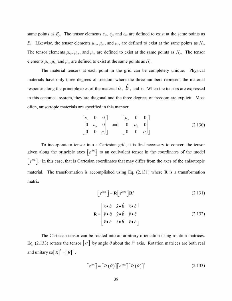
The material tensors at each point in the grid can be completely unique. Physical
materials have only three degrees of freedom where the three numbers represent the material
response along the principle axes of the material a , b , and c . When the tensors are expressed
in this canonical system, they are diagonal and the three degrees of freedom are explicit. Most
often, anisotropic materials are specified in this manner.
0 0 0 0
0 0 and 0 0
0 0 0 0
a a
b b
c c
(2.130)
To incorporate a tensor into a Cartesian grid, it is first necessary to convert the tensor
given along the principle axes abc to an equivalent tensor in the coordinates of the model
xyz . In this case, that is Cartesian coordinates that may differ from the axes of the anisotropic
material. The transformation is accomplished using Eq. (2.131) where R is a transformation
matrix
xyz abc T R R (2.131)
ˆˆ ˆ ˆ ˆ ˆ
ˆˆ ˆ ˆ ˆ ˆ
ˆˆ ˆˆ ˆ ˆ
x a x b x c
y a y b y c
z a z b z c
R (2.132)
The Cartesian tensor can be rotated into an arbitrary orientation using rotation matrices.
Eq. (2.133) rotates the tensor by angle θ about the ith
axis. Rotation matrices are both real
and unitary so 1T
R R
.
rot xyz T
i iR R (2.133)
39
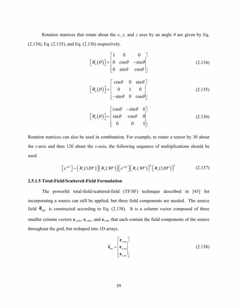
Rotation matrices that rotate about the x, y, and z axes by an angle θ are given by Eq.
(2.134), Eq. (2.135), and Eq. (2.136) respectively.
1 0 0
0 cos sin
0 sin cos
xR
(2.134)
cos 0 sin
0 1 0
sin 0 cos
yR
(2.135)
cos sin 0
sin cos 0
0 0 1
zR
(2.136)
Rotation matrices can also be used in combination. For example, to rotate a tensor by 30 about
the z-axis and then 120 about the x-axis, the following sequence of multiplications should be
used.
rot xyz120 30 30 120T T
x z z xR R R R (2.137)
2.5.1.5 Total-Field/Scattered-Field Formulation
The powerful total-field/scattered-field (TF/SF) technique described in [43] for
incorporating a source can still be applied, but three field components are needed. The source
field srce is constructed according to Eq. (2.138). It is a column vector composed of three
smaller column vectors ex,src, ey,src, and ez,src that each contain the field components of the source
throughout the grid, but reshaped into 1D arrays.
,src
src ,src
,src
x
y
z
e
e e
e
(2.138)
40
1,1,11,1,1 1,1,1
,src,src ,src
1,1,21,1,2 1,1,2
,src,src ,src
,src ,src ,src
, ,, , , ,
,src,src ,src
x y zx y z x y z
yx z
yx z
x y z
N N NN N N N N N
yx z
ee e
ee e
ee e
e e e (2.139)
The masking matrix Q is constructed to be in the form of Eq. (2.140). It is a block
diagonal matrix composed of three matrices along its diagonal. Qx is the scattered-field masking
for the Ex field, Qy is the scattered-field masking matrix for Ey field, and Qz is the scattered-field
masking matrix for the Ez field.
x
y
z
Q 0 0
Q 0 Q 0
0 0 Q
(2.140)
Given the wave matrix A, source field fsrc, and the masking matrix Q, the source vector b
is calculated according to
src b QA AQ e (2.141)
Now that a source has been incorporated, the field is calculated according to Eq. (2.142).
Note that e must be parsed to extract the individual components ex, ey, and ez. These three terms
can then then be reshaped back to the original grid.
1
x
y
z
e
e e A b
e
(2.142)
If needed, the magnetic field can be calculated using Eq. (2.126). This is
1 e
r
h μ C e (2.143)
41
2.5.2 Benchmark Simulation
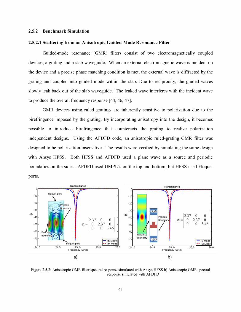
2.5.2.1 Scattering from an Anisotropic Guided-Mode Resonance Filter
Guided-mode resonance (GMR) filters consist of two electromagnetically coupled
devices; a grating and a slab waveguide. When an external electromagnetic wave is incident on
the device and a precise phase matching condition is met, the external wave is diffracted by the
grating and coupled into guided mode within the slab. Due to reciprocity, the guided waves
slowly leak back out of the slab waveguide. The leaked wave interferes with the incident wave
to produce the overall frequency response [44, 46, 47].
GMR devices using ruled gratings are inherently sensitive to polarization due to the
birefringence imposed by the grating. By incorporating anisotropy into the design, it becomes
possible to introduce birefringence that counteracts the grating to realize polarization
independent designs. Using the AFDFD code, an anisotropic ruled-grating GMR filter was
designed to be polarization insensitive. The results were verified by simulating the same design
with Ansys HFSS. Both HFSS and AFDFD used a plane wave as a source and periodic
boundaries on the sides. AFDFD used UMPL’s on the top and bottom, but HFSS used Floquet
ports.
Figure 2.5.2: Anisotropic GMR filter spectral response simulated with Ansys HFSS b) Anisotropic GMR spectral
response simulated with AFDFD
42
Figure 2.5.2 depicts the spectral response of an anisotropic GMR filter. Both the
transvers electric (TE) and transvers magnetic (TM) modes were made resonant at the same
frequency. Using the method presented in Chapter 3, a device could be realized using an
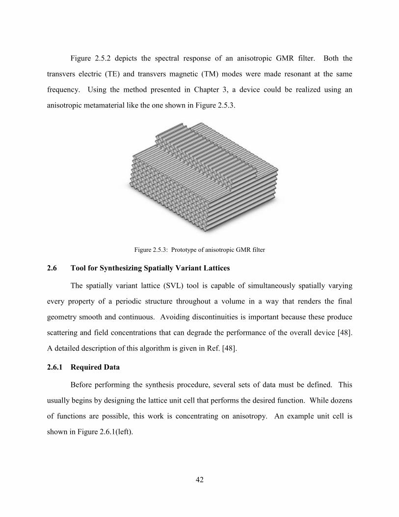
anisotropic metamaterial like the one shown in Figure 2.5.3.
Figure 2.5.3: Prototype of anisotropic GMR filter
2.6 Tool for Synthesizing Spatially Variant Lattices
The spatially variant lattice (SVL) tool is capable of simultaneously spatially varying
every property of a periodic structure throughout a volume in a way that renders the final
geometry smooth and continuous. Avoiding discontinuities is important because these produce
scattering and field concentrations that can degrade the performance of the overall device [48].
A detailed description of this algorithm is given in Ref. [48].
2.6.1 Required Data
Before performing the synthesis procedure, several sets of data must be defined. This
usually begins by designing the lattice unit cell that performs the desired function. While dozens
of functions are possible, this work is concentrating on anisotropy. An example unit cell is
shown in Figure 2.6.1(left).
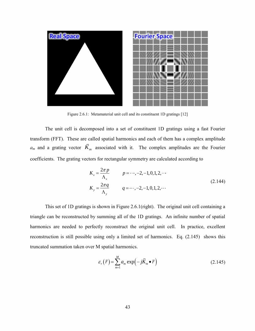
43
Figure 2.6.1: Metamaterial unit cell and its constituent 1D gratings [12]
The unit cell is decomposed into a set of constituent 1D gratings using a fast Fourier
transform (FFT). These are called spatial harmonics and each of them has a complex amplitude
am and a grating vector mK associated with it. The complex amplitudes are the Fourier
coefficients. The grating vectors for rectangular symmetry are calculated according to
2 , 2, 1,0,1,2,
2 , 2, 1,0,1,2,
x
x
y
y
pK p
qK q
(2.144)
This set of 1D gratings is shown in Figure 2.6.1(right). The original unit cell containing a
triangle can be reconstructed by summing all of the 1D gratings. An infinite number of spatial
harmonics are needed to perfectly reconstruct the original unit cell. In practice, excellent
reconstruction is still possible using only a limited set of harmonics. Eq. (2.145) shows this
truncated summation taken over M spatial harmonics.
1
expM
r m m
m
r a jK r
(2.145)
44
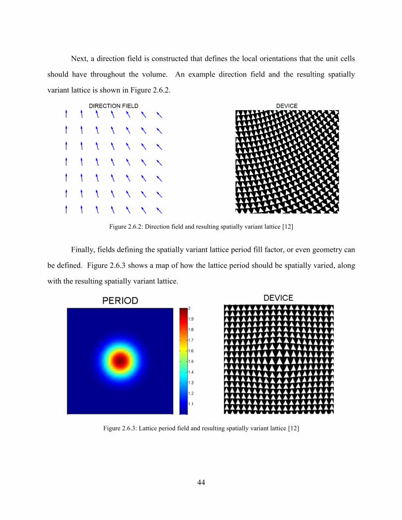
Next, a direction field is constructed that defines the local orientations that the unit cells
should have throughout the volume. An example direction field and the resulting spatially
variant lattice is shown in Figure 2.6.2.
Figure 2.6.2: Direction field and resulting spatially variant lattice [12]
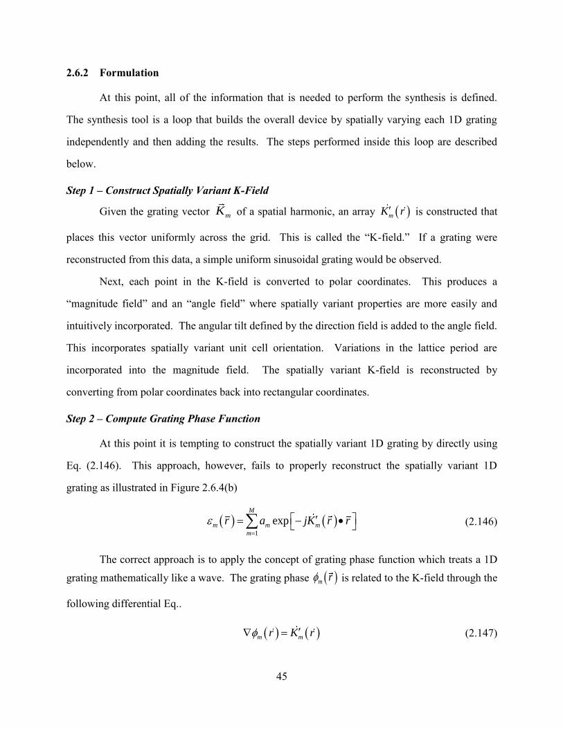
Finally, fields defining the spatially variant lattice period fill factor, or even geometry can
be defined. Figure 2.6.3 shows a map of how the lattice period should be spatially varied, along
with the resulting spatially variant lattice.
Figure 2.6.3: Lattice period field and resulting spatially variant lattice [12]
45
2.6.2 Formulation
At this point, all of the information that is needed to perform the synthesis is defined.
The synthesis tool is a loop that builds the overall device by spatially varying each 1D grating
independently and then adding the results. The steps performed inside this loop are described
below.
Step 1 – Construct Spatially Variant K-Field
Given the grating vector mK of a spatial harmonic, an array mK r is constructed that
places this vector uniformly across the grid. This is called the “K-field.” If a grating were
reconstructed from this data, a simple uniform sinusoidal grating would be observed.
Next, each point in the K-field is converted to polar coordinates. This produces a
“magnitude field” and an “angle field” where spatially variant properties are more easily and
intuitively incorporated. The angular tilt defined by the direction field is added to the angle field.
This incorporates spatially variant unit cell orientation. Variations in the lattice period are
incorporated into the magnitude field. The spatially variant K-field is reconstructed by
converting from polar coordinates back into rectangular coordinates.
Step 2 – Compute Grating Phase Function
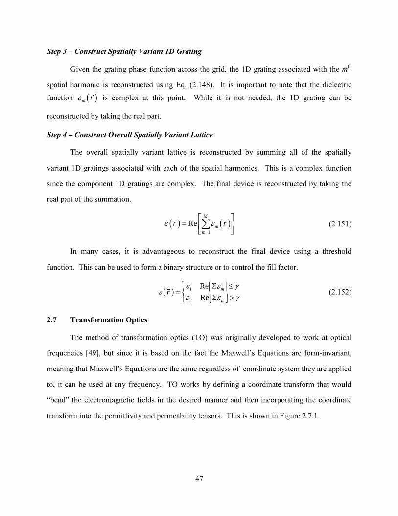
At this point it is tempting to construct the spatially variant 1D grating by directly using
Eq. (2.146). This approach, however, fails to properly reconstruct the spatially variant 1D
grating as illustrated in Figure 2.6.4(b)
1
expM
m m m
m
r a jK r r
(2.146)
The correct approach is to apply the concept of grating phase function which treats a 1D
grating mathematically like a wave. The grating phase m r is related to the K-field through the
following differential Eq..
m mr K r (2.147)
46
Figure 2.6.4(c) shows the grating phase function that was calculated from the K-field
shown in Figure 2.6.4(a). To correctly reconstruct the 1D grating, Eq. (2.148) is solved for and
then the grating phase term is directly used to reconstruct the grating according to
expm m mr a j r (2.148)
Figure 2.6.4.: Correct method for generating spatially variant 1D gratings [12]
Eq. (2.147) was solved for the grating phase using the finite-difference method. The
derivatives in this equation were approximated using finite-differences. The resulting equation is
written for each point in the grid. This large set of equations is written in matrix form as
,
,
,
x x m
y m y m
z z m
D K
D Φ K
D K
(2.149)
The term mΦ is a column vector containing the grating phase at each point on the grid.
These are not known at this point, but will be solved for shortly. The terms Dx, Dy, and Dz are
banded matrices that perform derivative operations across the grid. The terms Kx,m, Ky,m, and
Kz,m are diagonal matrices containing the components of the K-field across the grid. This matrix
equation is solved for the grating phase as follows.
1
,
,
,
x x m
m y y m
z z m
D K
Φ D K
D K
(2.150)
47
Step 3 – Construct Spatially Variant 1D Grating
Given the grating phase function across the grid, the 1D grating associated with the mth
spatial harmonic is reconstructed using Eq. (2.148). It is important to note that the dielectric
function m r is complex at this point. While it is not needed, the 1D grating can be
reconstructed by taking the real part.
Step 4 – Construct Overall Spatially Variant Lattice
The overall spatially variant lattice is reconstructed by summing all of the spatially
variant 1D gratings associated with each of the spatial harmonics. This is a complex function
since the component 1D gratings are complex. The final device is reconstructed by taking the
real part of the summation.
1
ReM
m
m
r r
(2.151)
In many cases, it is advantageous to reconstruct the final device using a threshold
function. This can be used to form a binary structure or to control the fill factor.
1
2
Re
Re
m
m
r
(2.152)
2.7 Transformation Optics
The method of transformation optics (TO) was originally developed to work at optical
frequencies [49], but since it is based on the fact the Maxwell’s Equations are form-invariant,
meaning that Maxwell’s Equations are the same regardless of coordinate system they are applied
to, it can be used at any frequency. TO works by defining a coordinate transform that would
“bend” the electromagnetic fields in the desired manner and then incorporating the coordinate
transform into the permittivity and permeability tensors. This is shown in Figure 2.7.1.
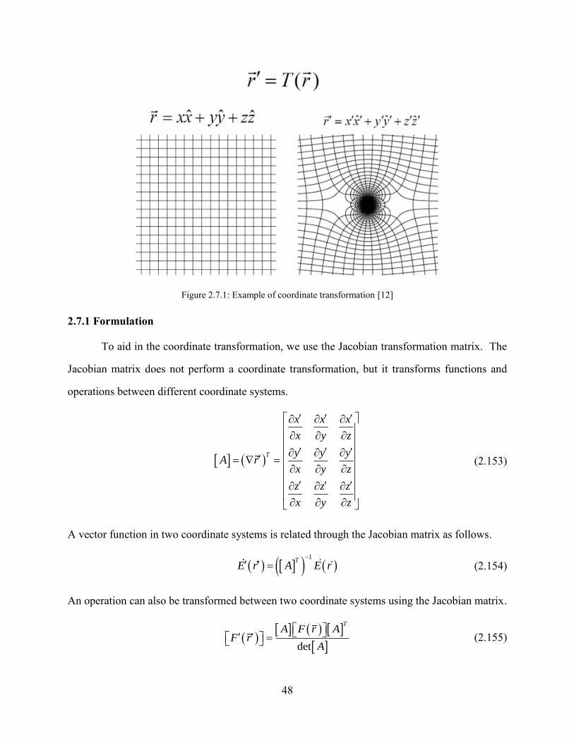
48
Figure 2.7.1: Example of coordinate transformation [12]
2.7.1 Formulation
To aid in the coordinate transformation, we use the Jacobian transformation matrix. The
Jacobian matrix does not perform a coordinate transformation, but it transforms functions and
operations between different coordinate systems.
T
x x x
x y z
y y yA r
x y z
z z z
x y z
(2.153)
A vector function in two coordinate systems is related through the Jacobian matrix as follows.
1
TE r A E r
(2.154)
An operation can also be transformed between two coordinate systems using the Jacobian matrix.
det
TA F r A
F rA
(2.155)

49
Since Maxwell’s equations are form-invariant, the coordinate transform can be absorbed solely
into the material properties. In any coordinate system Maxwell’s equations can be written as
H j E (2.156)
E j H (2.157)
Now, we apply a coordinate transform to Maxwell’s equations and absorb that into the material
properties. This result is Maxwell’s equations again, but with modified constitutive parameters.
H j E (2.158)
E j H (2.159)
This can be easily proven. Defining the coordinate transformation as:
r r r (2.160)
We now have
1
TE r A E r
(2.161)
1
TH r A H r
(2.162)
det
TA r A
rA
(2.163)
Substituting our functions transforms into Eq. (2.159).
1
1det
T T TA E j A A A A H
(2.164)
Equation (2.164) can be rewritten as
det
TA A
E j HA
(2.165)
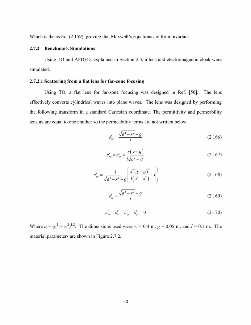
50
Which is the as Eq. (2.159), proving that Maxwell’s equations are form invariant.
2.7.2 Benchmark Simulations
Using TO and AFDFD, explained in Section 2.5, a lens and electromagnetic cloak were
simulated.
2.7.2.1 Scattering from a flat lens for far-zone focusing
Using TO, a flat lens for far-zone focusing was designed in Ref. [50]. The lens
effectively converts cylindrical waves into plane waves. The lens was designed by performing
the following transform in a standard Cartesian coordinate. The permittivity and permeability
tensors are equal to one another so the permeability terms are not written below.
2 2
xx
a x g
l
(2.166)
2 2xy yx
x y g
l a x
(2.167)
22
2 22 2
1yy
x y gl
l a xa x g
(2.168)
2 2
zz
a x g
l
(2.169)
0zx xz zy yz (2.170)
Where a = (g2 + w
2)1/2
. The dimensions used were w = 0.4 m, g = 0.05 m, and l = 0.1 m. The
material parameters are shown in Figure 2.7.2.
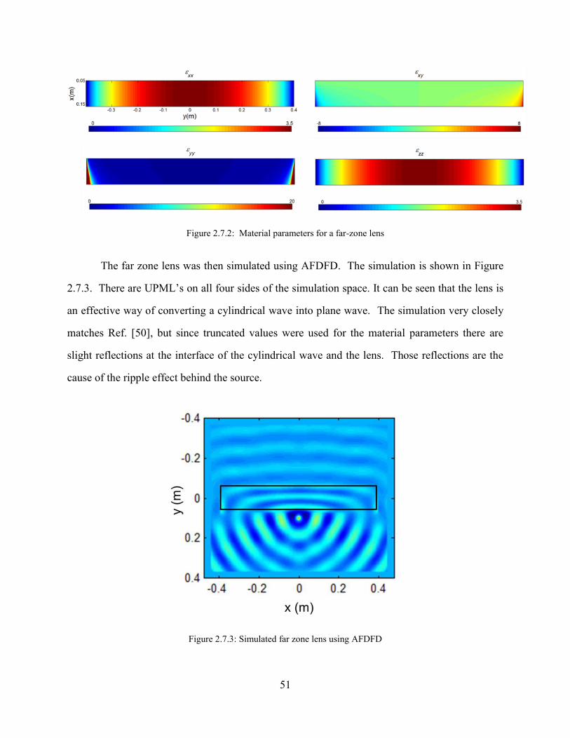
51
Figure 2.7.2: Material parameters for a far-zone lens
The far zone lens was then simulated using AFDFD. The simulation is shown in Figure
2.7.3. There are UPML’s on all four sides of the simulation space. It can be seen that the lens is
an effective way of converting a cylindrical wave into plane wave. The simulation very closely
matches Ref. [50], but since truncated values were used for the material parameters there are
slight reflections at the interface of the cylindrical wave and the lens. Those reflections are the
cause of the ripple effect behind the source.
Figure 2.7.3: Simulated far zone lens using AFDFD
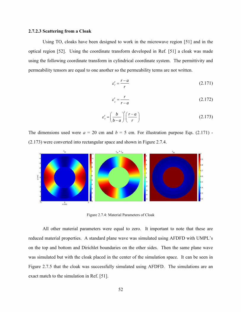
52
2.7.2.3 Scattering from a Cloak
Using TO, cloaks have been designed to work in the microwave region [51] and in the
optical region [52]. Using the coordinate transform developed in Ref. [51] a cloak was made
using the following coordinate transform in cylindrical coordinate system. The permittivity and
permeability tensors are equal to one another so the permeability terms are not written.
r
r a
r
(2.171)
r
r a
(2.172)
2
z
b r a
b a r
(2.173)
The dimensions used were a = 20 cm and b = 5 cm. For illustration purpose Eqs. (2.171) -
(2.173) were converted into rectangular space and shown in Figure 2.7.4.
Figure 2.7.4: Material Parameters of Cloak
All other material parameters were equal to zero. It important to note that these are
reduced material properties. A standard plane wave was simulated using AFDFD with UMPL’s
on the top and bottom and Dirichlet boundaries on the other sides. Then the same plane wave
was simulated but with the cloak placed in the center of the simulation space. It can be seen in
Figure 2.7.5 that the cloak was successfully simulated using AFDFD. The simulations are an
exact match to the simulation in Ref. [51].
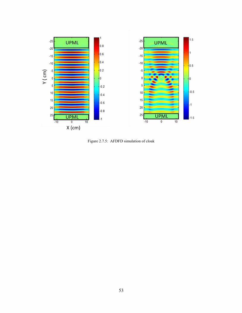
53
Figure 2.7.5: AFDFD simulation of cloak
54
Chapter 3: 3D Printing of Anisotropic Metamaterials
This chapter summarizes an artificially anisotropic metamaterial manufactured by 3D
printing. First, the design methodology and optimization of a uniaxial metamaterial is discussed.
Second, samples were manufactured using FDM and their dielectric tensor properties measured
in the lab. The measured results agree well with the model predictions.
3.1 Device Design
The PWEM, derived in section 2.3, was used to predict the effective tensor parameters of
the anisotropic metamaterial. The method discretizes Maxwell’s equations by expanding the
field into a plane wave basis. This is highly efficient for all-dielectric structures with low to
moderate dielectric contrast. Retrieving the constitutive parameters was simple because our
structures operate in the long wavelength limit where branching [53, 54] does not occur. Given
the dielectric function r of the unit cell and a Bloch wave vector , the PWEM solves
Maxwell’s equations as an eigen-value problem where the eigen-value is square of the free space
wave number 2
0k . To ensure the model operates in the long wavelength limit, the magnitude of
the Bloch wave vector was made very small (i.e. β< 0.1/a). The effective refractive index of a
Bloch wave can be calculated using Eq. (3.1) by dividing the magnitude of the Bloch wave
vector by the wave number of the first order band [54].
eff 0n k k (3.1)
In this work, an all-dielectric uniaxial metamaterial was designed. Being uniform in the
z-direction, it was possible to model the device using a 2D PWEM code. In this case, Maxwell’s
equations decouple into two distinct modes, TM and TE. The TE mode has the electric field
polarized in the x-y plane while the TM mode has the electric field polarized perpendicular to
this plane. The ordinary refractive index no was retrieved by using a Bloch wave vector confined
to the x-y plane. The direction in this plane was arbitrary due to the structure having uniaxial
symmetry. The extraordinary refractive index ne was retrieved using a Bloch wave vector
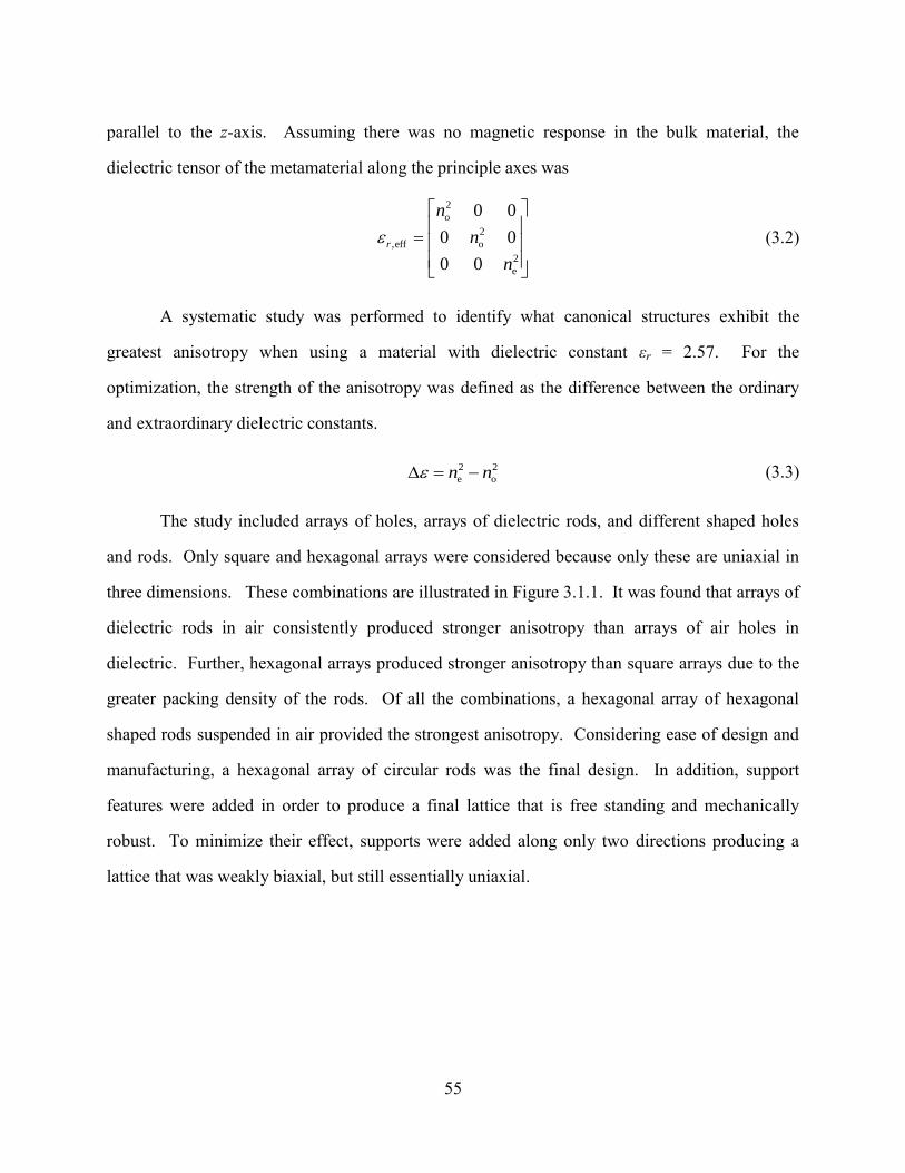
55
parallel to the z-axis. Assuming there was no magnetic response in the bulk material, the
dielectric tensor of the metamaterial along the principle axes was
2
o
2
,eff o
2
e
0 0
0 0
0 0
r
n
n
n
(3.2)
A systematic study was performed to identify what canonical structures exhibit the
greatest anisotropy when using a material with dielectric constant εr = 2.57. For the
optimization, the strength of the anisotropy was defined as the difference between the ordinary
and extraordinary dielectric constants.
2 2
e on n (3.3)
The study included arrays of holes, arrays of dielectric rods, and different shaped holes
and rods. Only square and hexagonal arrays were considered because only these are uniaxial in
three dimensions. These combinations are illustrated in Figure 3.1.1. It was found that arrays of
dielectric rods in air consistently produced stronger anisotropy than arrays of air holes in
dielectric. Further, hexagonal arrays produced stronger anisotropy than square arrays due to the
greater packing density of the rods. Of all the combinations, a hexagonal array of hexagonal
shaped rods suspended in air provided the strongest anisotropy. Considering ease of design and
manufacturing, a hexagonal array of circular rods was the final design. In addition, support
features were added in order to produce a final lattice that is free standing and mechanically
robust. To minimize their effect, supports were added along only two directions producing a
lattice that was weakly biaxial, but still essentially uniaxial.
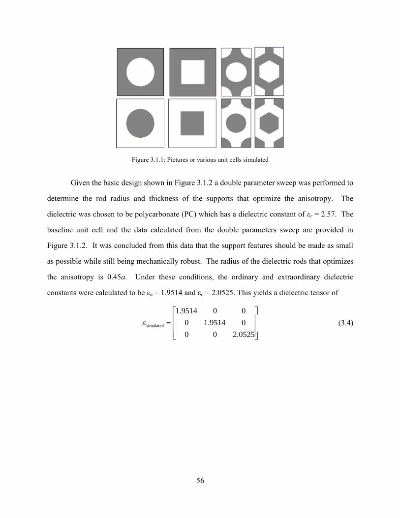
56
Figure 3.1.1: Pictures or various unit cells simulated
Given the basic design shown in Figure 3.1.2 a double parameter sweep was performed to
determine the rod radius and thickness of the supports that optimize the anisotropy. The
dielectric was chosen to be polycarbonate (PC) which has a dielectric constant of εr = 2.57. The
baseline unit cell and the data calculated from the double parameters sweep are provided in
Figure 3.1.2. It was concluded from this data that the support features should be made as small
as possible while still being mechanically robust. The radius of the dielectric rods that optimizes
the anisotropy is 0.45a. Under these conditions, the ordinary and extraordinary dielectric
constants were calculated to be εo = 1.9514 and εe = 2.0525. This yields a dielectric tensor of
simulated
1.9514 0 0
0 1.9514 0
0 0 2.0525
(3.4)
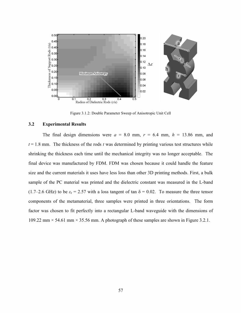
57
Figure 3.1.2: Double Parameter Sweep of Anisotropic Unit Cell
3.2 Experimental Results
The final design dimensions were a = 8.0 mm, r = 6.4 mm, h = 13.86 mm, and
t = 1.8 mm. The thickness of the rods t was determined by printing various test structures while
shrinking the thickness each time until the mechanical integrity was no longer acceptable. The
final device was manufactured by FDM. FDM was chosen because it could handle the feature
size and the current materials it uses have less loss than other 3D printing methods. First, a bulk
sample of the PC material was printed and the dielectric constant was measured in the L-band
(1.7–2.6 GHz) to be εr = 2.57 with a loss tangent of tan δ = 0.02. To measure the three tensor
components of the metamaterial, three samples were printed in three orientations. The form
factor was chosen to fit perfectly into a rectangular L-band waveguide with the dimensions of
109.22 mm × 54.61 mm × 35.56 mm. A photograph of these samples are shown in Figure 3.2.1.
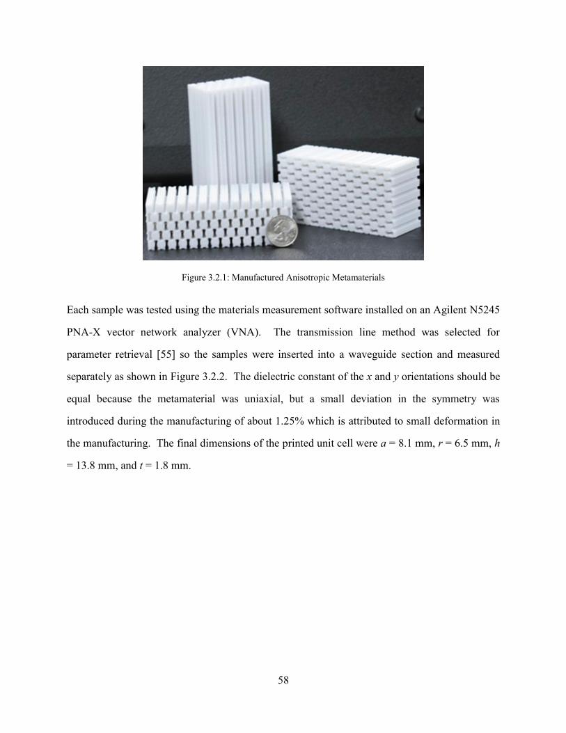
58
Figure 3.2.1: Manufactured Anisotropic Metamaterials
Each sample was tested using the materials measurement software installed on an Agilent N5245
PNA-X vector network analyzer (VNA). The transmission line method was selected for
parameter retrieval [55] so the samples were inserted into a waveguide section and measured
separately as shown in Figure 3.2.2. The dielectric constant of the x and y orientations should be
equal because the metamaterial was uniaxial, but a small deviation in the symmetry was
introduced during the manufacturing of about 1.25% which is attributed to small deformation in
the manufacturing. The final dimensions of the printed unit cell were a = 8.1 mm, r = 6.5 mm, h
= 13.8 mm, and t = 1.8 mm.
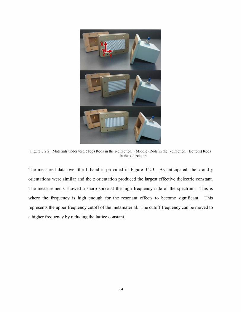
59
Figure 3.2.2: Materials under test. (Top) Rods in the z-direction. (Middle) Rods in the y-direction. (Bottom) Rods
in the x-direction
The measured data over the L-band is provided in Figure 3.2.3. As anticipated, the x and y
orientations were similar and the z orientation produced the largest effective dielectric constant.
The measurements showed a sharp spike at the high frequency side of the spectrum. This is
where the frequency is high enough for the resonant effects to become significant. This
represents the upper frequency cutoff of the metamaterial. The cutoff frequency can be moved to
a higher frequency by reducing the lattice constant.
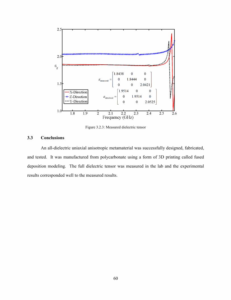
60
Figure 3.2.3: Measured dielectric tensor
3.3 Conclusions
An all-dielectric uniaxial anisotropic metamaterial was successfully designed, fabricated,
and tested. It was manufactured from polycarbonate using a form of 3D printing called fused
deposition modeling. The full dielectric tensor was measured in the lab and the experimental
results corresponded well to the measured results.
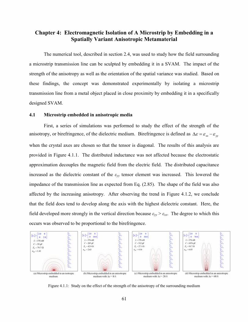
61
Chapter 4: Electromagnetic Isolation of A Microstrip by Embedding in a
Spatially Variant Anisotropic Metamaterial
The numerical tool, described in section 2.4, was used to study how the field surrounding
a microstrip transmission line can be sculpted by embedding it in a SVAM. The impact of the
strength of the anisotropy as well as the orientation of the spatial variance was studied. Based on
these findings, the concept was demonstrated experimentally by isolating a microstrip
transmission line from a metal object placed in close proximity by embedding it in a specifically
designed SVAM.
4.1 Microstrip embedded in anisotropic media
First, a series of simulations was performed to study the effect of the strength of the
anisotropy, or birefringence, of the dielectric medium. Birefringence is defined as xx yy
when the crystal axes are chosen so that the tensor is diagonal. The results of this analysis are
provided in Figure 4.1.1. The distributed inductance was not affected because the electrostatic
approximation decouples the magnetic field from the electric field. The distributed capacitance
increased as the dielectric constant of the εyy tensor element was increased. This lowered the
impedance of the transmission line as expected from Eq. (2.85). The shape of the field was also
affected by the increasing anisotropy. After observing the trend in Figure 4.1.2, we conclude
that the field does tend to develop along the axis with the highest dielectric constant. Here, the
field developed more strongly in the vertical direction because εyy > εxx. The degree to which this
occurs was observed to be proportional to the birefringence.
Figure 4.1.1: Study on the effect of the strength of the anisotropy of the surrounding medium
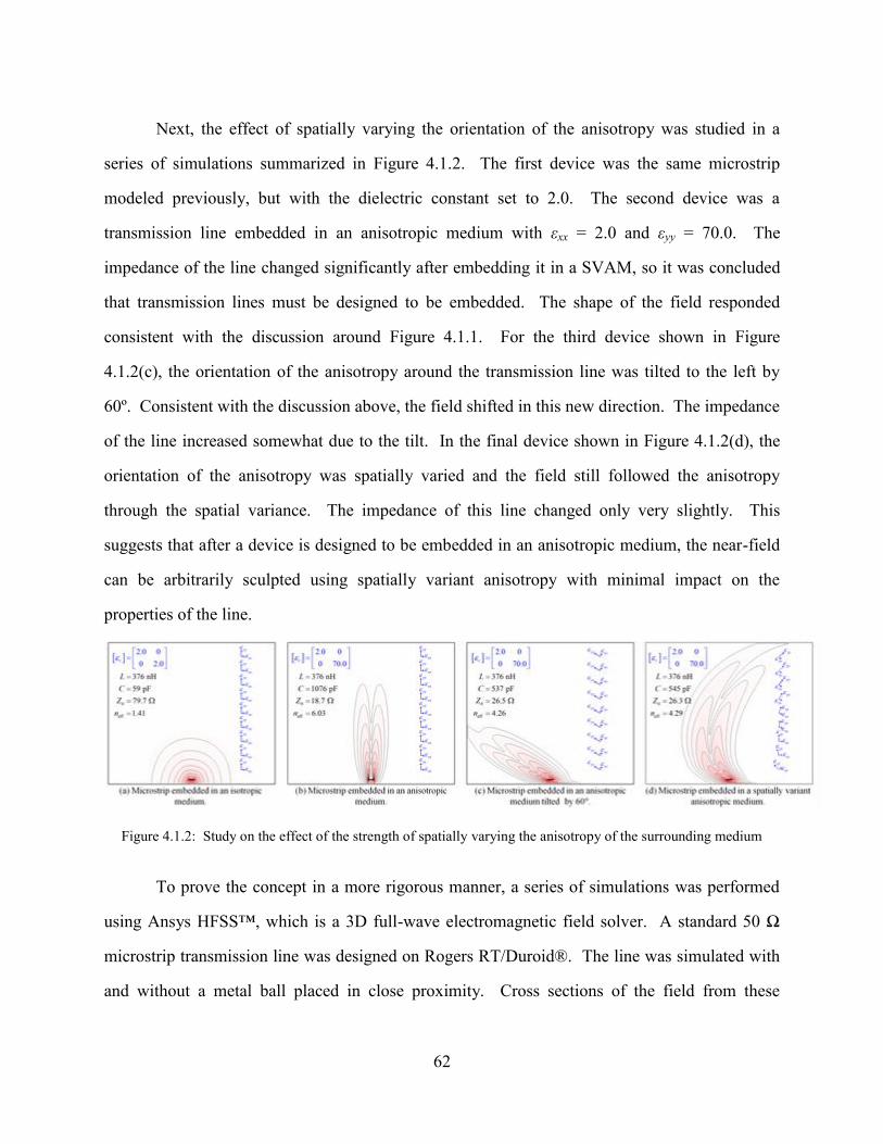
62
Next, the effect of spatially varying the orientation of the anisotropy was studied in a
series of simulations summarized in Figure 4.1.2. The first device was the same microstrip
modeled previously, but with the dielectric constant set to 2.0. The second device was a
transmission line embedded in an anisotropic medium with εxx = 2.0 and εyy = 70.0. The
impedance of the line changed significantly after embedding it in a SVAM, so it was concluded
that transmission lines must be designed to be embedded. The shape of the field responded
consistent with the discussion around Figure 4.1.1. For the third device shown in Figure
4.1.2(c), the orientation of the anisotropy around the transmission line was tilted to the left by
60º. Consistent with the discussion above, the field shifted in this new direction. The impedance
of the line increased somewhat due to the tilt. In the final device shown in Figure 4.1.2(d), the
orientation of the anisotropy was spatially varied and the field still followed the anisotropy
through the spatial variance. The impedance of this line changed only very slightly. This
suggests that after a device is designed to be embedded in an anisotropic medium, the near-field
can be arbitrarily sculpted using spatially variant anisotropy with minimal impact on the
properties of the line.
Figure 4.1.2: Study on the effect of the strength of spatially varying the anisotropy of the surrounding medium
To prove the concept in a more rigorous manner, a series of simulations was performed
using Ansys HFSS™, which is a 3D full-wave electromagnetic field solver. A standard 50 Ω
microstrip transmission line was designed on Rogers RT/Duroid®. The line was simulated with
and without a metal ball placed in close proximity. Cross sections of the field from these
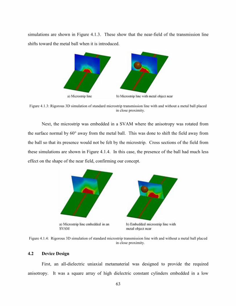
63
simulations are shown in Figure 4.1.3. These show that the near-field of the transmission line
shifts toward the metal ball when it is introduced.
Figure 4.1.3: Rigorous 3D simulation of standard microstrip transmission line with and without a metal ball placed
in close proximity.
Next, the microstrip was embedded in a SVAM where the anisotropy was rotated from
the surface normal by 60° away from the metal ball. This was done to shift the field away from
the ball so that its presence would not be felt by the microstrip. Cross sections of the field from
these simulations are shown in Figure 4.1.4. In this case, the presence of the ball had much less
effect on the shape of the near field, confirming our concept.
Figure 4.1.4: Rigorous 3D simulation of standard microstrip transmission line with and without a metal ball placed
in close proximity.
4.2 Device Design
First, an all-dielectric uniaxial metamaterial was designed to provide the required
anisotropy. It was a square array of high dielectric constant cylinders embedded in a low
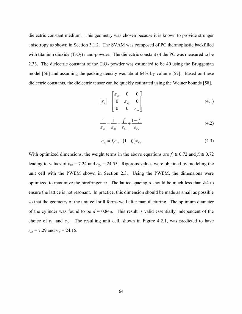
64
dielectric constant medium. This geometry was chosen because it is known to provide stronger
anisotropy as shown in Section 3.1.2. The SVAM was composed of PC thermoplastic backfilled
with titanium dioxide (TiO2) nano-powder. The dielectric constant of the PC was measured to be
2.33. The dielectric constant of the TiO2 powder was estimated to be 40 using the Bruggeman
model [56] and assuming the packing density was about 64% by volume [57]. Based on these
dielectric constants, the dielectric tensor can be quickly estimated using the Weiner bounds [58].
0 0
0 0
0 0
xx
r yy
zz
(4.1)
1 2
11 1 o o
xx zz r r
f f
(4.2)
1 21yy e r e rf f (4.3)
With optimized dimensions, the weight terms in the above equations are fo 0.72 and fe 0.72
leading to values of εxx = 7.24 and εyy = 24.55. Rigorous values were obtained by modeling the
unit cell with the PWEM shown in Section 2.3. Using the PWEM, the dimensions were
optimized to maximize the birefringence. The lattice spacing a should be much less than λ/4 to
ensure the lattice is not resonant. In practice, this dimension should be made as small as possible
so that the geometry of the unit cell still forms well after manufacturing. The optimum diameter
of the cylinder was found to be d = 0.84a. This result is valid essentially independent of the
choice of εr1 and εr2. The resulting unit cell, shown in Figure 4.2.1, was predicted to have
εxx = 7.29 and εyy = 24.15.
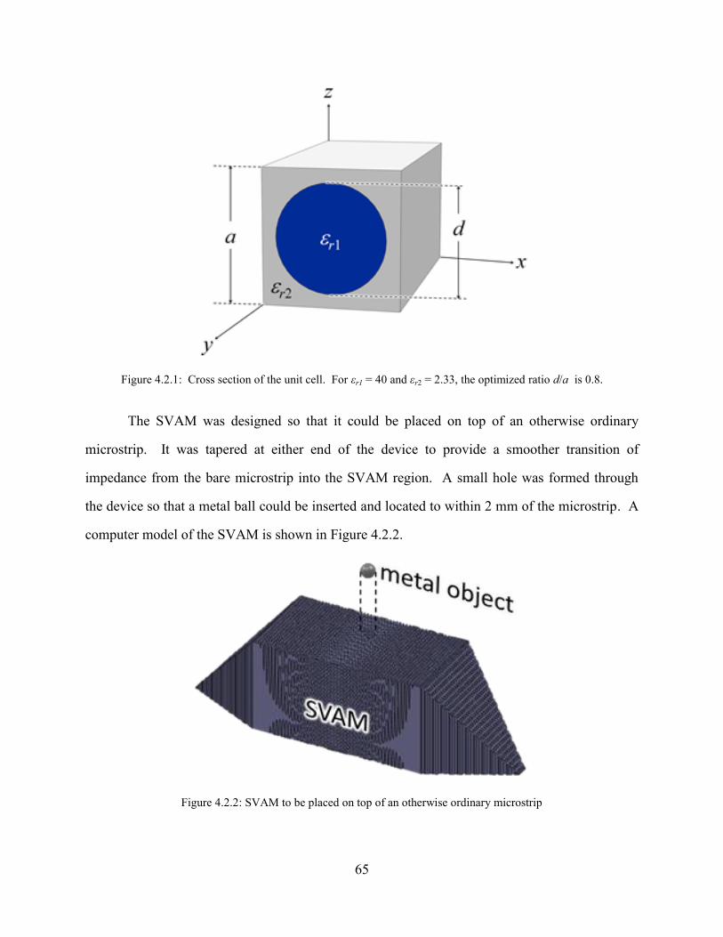
65
Figure 4.2.1: Cross section of the unit cell. For εr1 = 40 and εr2 = 2.33, the optimized ratio d/a is 0.8.
The SVAM was designed so that it could be placed on top of an otherwise ordinary
microstrip. It was tapered at either end of the device to provide a smoother transition of
impedance from the bare microstrip into the SVAM region. A small hole was formed through
the device so that a metal ball could be inserted and located to within 2 mm of the microstrip. A
computer model of the SVAM is shown in Figure 4.2.2.
Figure 4.2.2: SVAM to be placed on top of an otherwise ordinary microstrip
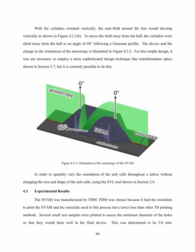
66
With the cylinders oriented vertically, the near-field around the line would develop
vertically as shown in Figure 4.2.1(b). To move the field away from the ball, the cylinders were
tilted away from the ball to an angle of 60° following a Gaussian profile. The device and the
change in the orientation of the anisotropy is illustrated in Figure 4.2.3. For this simple design, it
was not necessary to employ a more sophisticated design technique like transformation optics
shown in Section 2.7, but it is certainly possible to do this.
Figure 4.2.3: Orientation of the anisotropy of the SVAM
In order to spatially vary the orientation of the unit cells throughout a lattice without
changing the size and shape of the unit cells, using the SVL tool shown in Section 2.6.
4.3 Experimental Results
The SVAM was manufactured by FDM. FDM was chosen because it had the resolution
to print the SVAM and the materials used in this process have lower loss than other 3D printing
methods. Several small test samples were printed to assess the minimum diameter of the holes
so that they would form well in the final device. This was determined to be 2.0 mm.
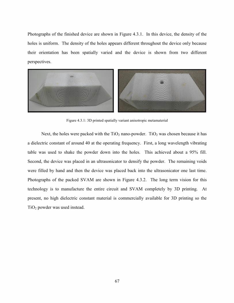
67
Photographs of the finished device are shown in Figure 4.3.1. In this device, the density of the
holes is uniform. The density of the holes appears different throughout the device only because
their orientation has been spatially varied and the device is shown from two different
perspectives.
Figure 4.3.1: 3D printed spatially variant anisotropic metamaterial
Next, the holes were packed with the TiO2 nano-powder. TiO2 was chosen because it has
a dielectric constant of around 40 at the operating frequency. First, a long wavelength vibrating
table was used to shake the powder down into the holes. This achieved about a 95% fill.
Second, the device was placed in an ultrasonicator to densify the powder. The remaining voids
were filled by hand and then the device was placed back into the ultrasonicator one last time.
Photographs of the packed SVAM are shown in Figure 4.3.2. The long term vision for this
technology is to manufacture the entire circuit and SVAM completely by 3D printing. At
present, no high dielectric constant material is commercially available for 3D printing so the
TiO2 powder was used instead.
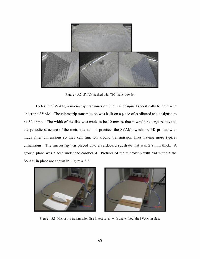
68
Figure 4.3.2: SVAM packed with TiO2 nano-powder
To test the SVAM, a microstrip transmission line was designed specifically to be placed
under the SVAM. The microstrip transmission was built on a piece of cardboard and designed to
be 50 ohms. The width of the line was made to be 10 mm so that it would be large relative to
the periodic structure of the metamaterial. In practice, the SVAMs would be 3D printed with
much finer dimensions so they can function around transmission lines having more typical
dimensions. The microstrip was placed onto a cardboard substrate that was 2.8 mm thick. A
ground plane was placed under the cardboard. Pictures of the microstrip with and without the
SVAM in place are shown in Figure 4.3.3.
Figure 4.3.3: Microstrip transmission line in test setup, with and without the SVAM in place
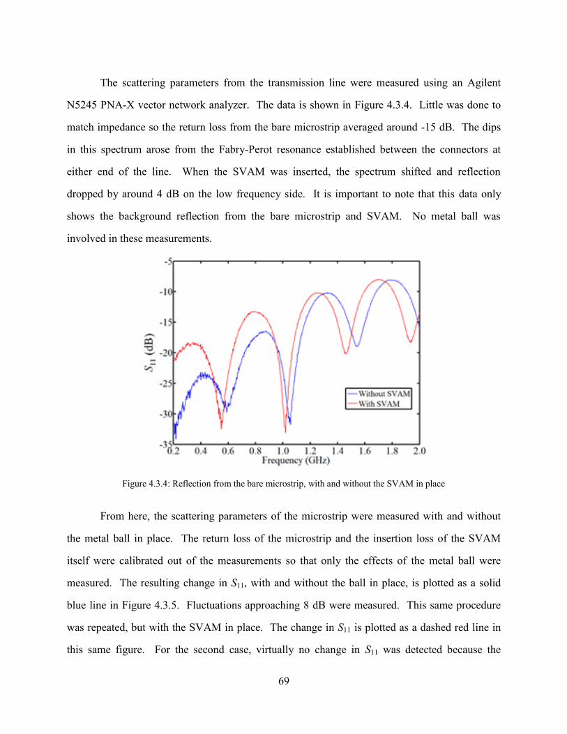
69
The scattering parameters from the transmission line were measured using an Agilent
N5245 PNA-X vector network analyzer. The data is shown in Figure 4.3.4. Little was done to
match impedance so the return loss from the bare microstrip averaged around -15 dB. The dips
in this spectrum arose from the Fabry-Perot resonance established between the connectors at
either end of the line. When the SVAM was inserted, the spectrum shifted and reflection
dropped by around 4 dB on the low frequency side. It is important to note that this data only
shows the background reflection from the bare microstrip and SVAM. No metal ball was
involved in these measurements.
Figure 4.3.4: Reflection from the bare microstrip, with and without the SVAM in place
From here, the scattering parameters of the microstrip were measured with and without
the metal ball in place. The return loss of the microstrip and the insertion loss of the SVAM
itself were calibrated out of the measurements so that only the effects of the metal ball were
measured. The resulting change in S11, with and without the ball in place, is plotted as a solid
blue line in Figure 4.3.5. Fluctuations approaching 8 dB were measured. This same procedure
was repeated, but with the SVAM in place. The change in S11 is plotted as a dashed red line in
this same figure. For the second case, virtually no change in S11 was detected because the
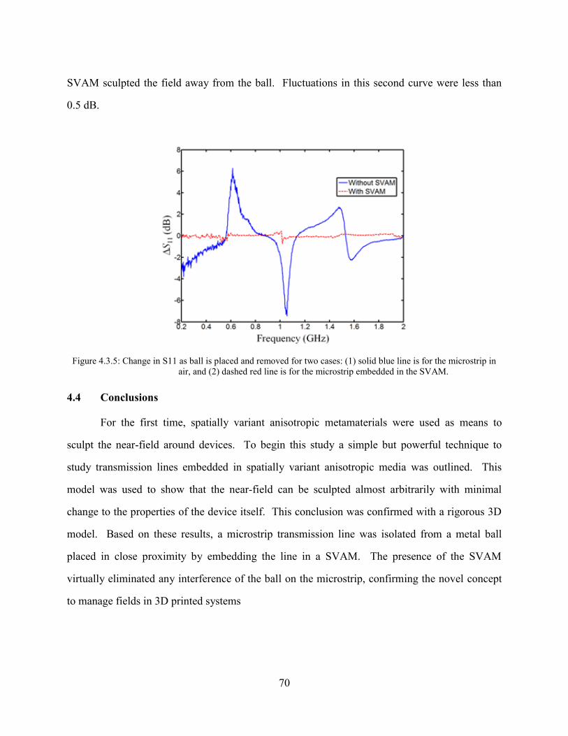
70
SVAM sculpted the field away from the ball. Fluctuations in this second curve were less than
0.5 dB.
Figure 4.3.5: Change in S11 as ball is placed and removed for two cases: (1) solid blue line is for the microstrip in
air, and (2) dashed red line is for the microstrip embedded in the SVAM.
4.4 Conclusions
For the first time, spatially variant anisotropic metamaterials were used as means to
sculpt the near-field around devices. To begin this study a simple but powerful technique to
study transmission lines embedded in spatially variant anisotropic media was outlined. This
model was used to show that the near-field can be sculpted almost arbitrarily with minimal
change to the properties of the device itself. This conclusion was confirmed with a rigorous 3D
model. Based on these results, a microstrip transmission line was isolated from a metal ball
placed in close proximity by embedding the line in a SVAM. The presence of the SVAM
virtually eliminated any interference of the ball on the microstrip, confirming the novel concept
to manage fields in 3D printed systems
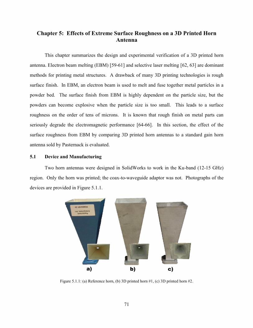
71
Chapter 5: Effects of Extreme Surface Roughness on a 3D Printed Horn
Antenna
This chapter summarizes the design and experimental verification of a 3D printed horn
antenna. Electron beam melting (EBM) [59-61] and selective laser melting [62, 63] are dominant
methods for printing metal structures. A drawback of many 3D printing technologies is rough
surface finish. In EBM, an electron beam is used to melt and fuse together metal particles in a
powder bed. The surface finish from EBM is highly dependent on the particle size, but the
powders can become explosive when the particle size is too small. This leads to a surface
roughness on the order of tens of microns. It is known that rough finish on metal parts can
seriously degrade the electromagnetic performance [64-66]. In this section, the effect of the
surface roughness from EBM by comparing 3D printed horn antennas to a standard gain horn
antenna sold by Pasternack is evaluated.
5.1 Device and Manufacturing
Two horn antennas were designed in SolidWorks to work in the Ku-band (12-15 GHz)
region. Only the horn was printed; the coax-to-waveguide adaptor was not. Photographs of the
devices are provided in Figure 5.1.1.
Figure 5.1.1: (a) Reference horn, (b) 3D printed horn #1, (c) 3D printed horn #2.
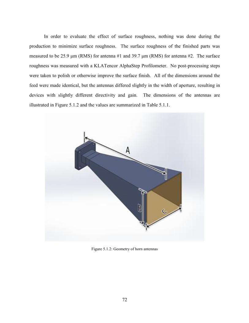
72
In order to evaluate the effect of surface roughness, nothing was done during the
production to minimize surface roughness. The surface roughness of the finished parts was
measured to be 25.9 μm (RMS) for antenna #1 and 39.7 μm (RMS) for antenna #2. The surface
roughness was measured with a KLATencor AlphaStep Profilometer. No post-processing steps
were taken to polish or otherwise improve the surface finish. All of the dimensions around the
feed were made identical, but the antennas differed slightly in the width of aperture, resulting in
devices with slightly different directivity and gain. The dimensions of the antennas are
illustrated in Figure 5.1.2 and the values are summarized in Table 5.1.1.
Figure 5.1.2: Geometry of horn antennas
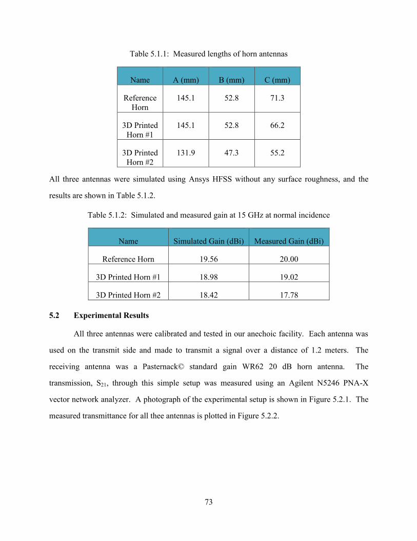
73
Table 5.1.1: Measured lengths of horn antennas
Name A (mm) B (mm) C (mm)
Reference
Horn
145.1 52.8 71.3
3D Printed
Horn #1
145.1 52.8 66.2
3D Printed
Horn #2
131.9 47.3 55.2
All three antennas were simulated using Ansys HFSS without any surface roughness, and the
results are shown in Table 5.1.2.
Table 5.1.2: Simulated and measured gain at 15 GHz at normal incidence
Name Simulated Gain (dBi) Measured Gain (dBi)
Reference Horn 19.56 20.00
3D Printed Horn #1 18.98 19.02
3D Printed Horn #2 18.42 17.78
5.2 Experimental Results
All three antennas were calibrated and tested in our anechoic facility. Each antenna was
used on the transmit side and made to transmit a signal over a distance of 1.2 meters. The
receiving antenna was a Pasternack© standard gain WR62 20 dB horn antenna. The
transmission, S21, through this simple setup was measured using an Agilent N5246 PNA-X
vector network analyzer. A photograph of the experimental setup is shown in Figure 5.2.1. The
measured transmittance for all thee antennas is plotted in Figure 5.2.2.
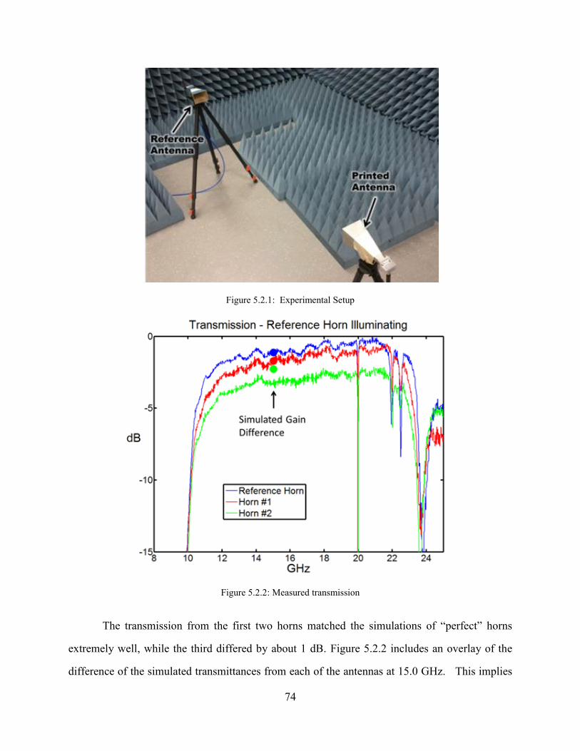
74
Figure 5.2.1: Experimental Setup
Figure 5.2.2: Measured transmission
The transmission from the first two horns matched the simulations of “perfect” horns
extremely well, while the third differed by about 1 dB. Figure 5.2.2 includes an overlay of the
difference of the simulated transmittances from each of the antennas at 15.0 GHz. This implies

75
that the difference in the S21 measurements between the reference horn and horn #1 was due to
their different directivities and not the surface roughness. Horn #2, which had a much rougher
surface than horn #1, experienced around a 1 dB loss, which was attributed to the surface
roughness.
5.4 Conclusions
To evaluate the impact of surface roughness resulting from 3D printing of metals, two
Ku-band horn antennas were 3D printed using EBM. No post-processing steps were taken to
polish or otherwise improve the surface finish, which was measured to be on the order of 20 to
40 microns. The antennas were experimentally tested and compared to a standard horn antenna
purchased from Pasternack. It was observed that the surface roughness of horn #1
(25.9 μm RMS) had no measurable effect on the performance. Horn #2 had almost twice
thesurface roughness (39.7 μm RMS) and measured a 1 dB loss.
76
Chapter 6: Electromagnetic Isolation of Cell Phone Antennas by Embedding
in a Spatially Variant Anisotropic Metamaterial
A SVAM was built into a cell phone case to reduce the electromagnetic interaction of
two cell phone antennas placed in close proximity. The antennas were designed and simulated in
HFSS and the SVAM decreased the envelope correlation coefficient (ECC) dramatically.
6.1 Envelope Correlation Coefficient
The envelope correlation coefficient (ECC), ρe, is the standard way to assess the degree to
which multiple antennas are coupled. When the ECC is large, the capacity of the system may
decrease [67]. There are two major ways to calculate the ECC. The most accurate way requires
the 3D field radiation pattern [25, 26, 67, 68]. The formula for calculating the ECC with the 3D
radiation is provided in Eq. (6.1).
2
1 2
4
2 2
1 2
4 4
, ,
, ,e
F F d
F d F d
(6.1)
,iF is the 3D field radiation pattern of the system when port i is excited, all other port are
perfectly matched, and denotes a Hermitian product [68]. An easier way to calculate the ECC
is by using the scattering parameters. It is not as accurate as Eq. (6.1), but is widely accepted as
a method to obtain the ECC [22-24, 68]. The formula for calculating the ECC with scattering
parameters is shown in Eq. (6.2).
2* *
11 12 21
2 2 2 2
11 21 22 121 1e
S S S
S S S S
(6.2)
The * denotes a complex conjugate operation.
An ECC of 0.5 is considered to be the borderline between a poor antenna system and
good antenna system. The antenna system is considered to be working better the closer the ECC
is to zero [68, 69].
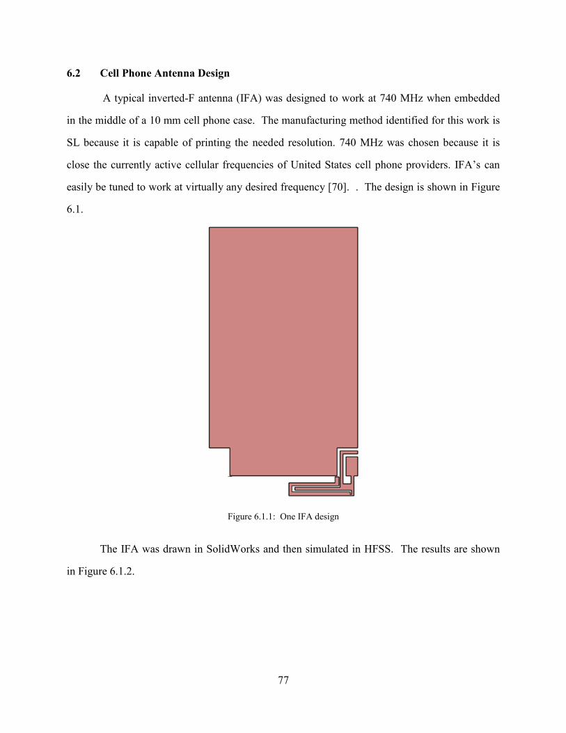
77
6.2 Cell Phone Antenna Design
A typical inverted-F antenna (IFA) was designed to work at 740 MHz when embedded
in the middle of a 10 mm cell phone case. The manufacturing method identified for this work is
SL because it is capable of printing the needed resolution. 740 MHz was chosen because it is
close the currently active cellular frequencies of United States cell phone providers. IFA’s can
easily be tuned to work at virtually any desired frequency [70]. . The design is shown in Figure
6.1.
Figure 6.1.1: One IFA design
The IFA was drawn in SolidWorks and then simulated in HFSS. The results are shown
in Figure 6.1.2.
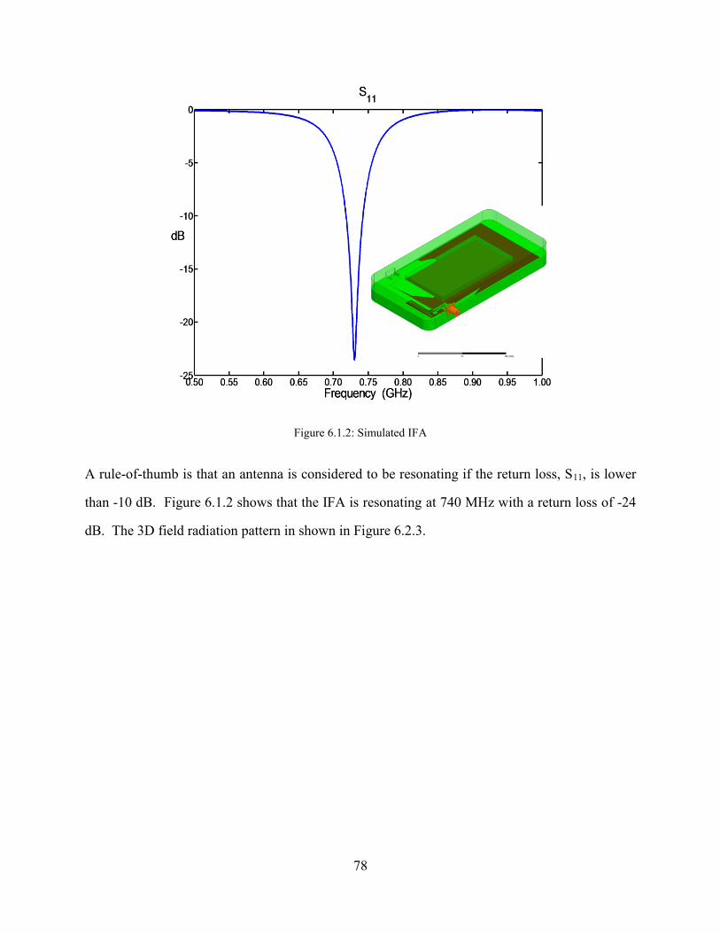
78
Figure 6.1.2: Simulated IFA
A rule-of-thumb is that an antenna is considered to be resonating if the return loss, S11, is lower
than -10 dB. Figure 6.1.2 shows that the IFA is resonating at 740 MHz with a return loss of -24
dB. The 3D field radiation pattern in shown in Figure 6.2.3.
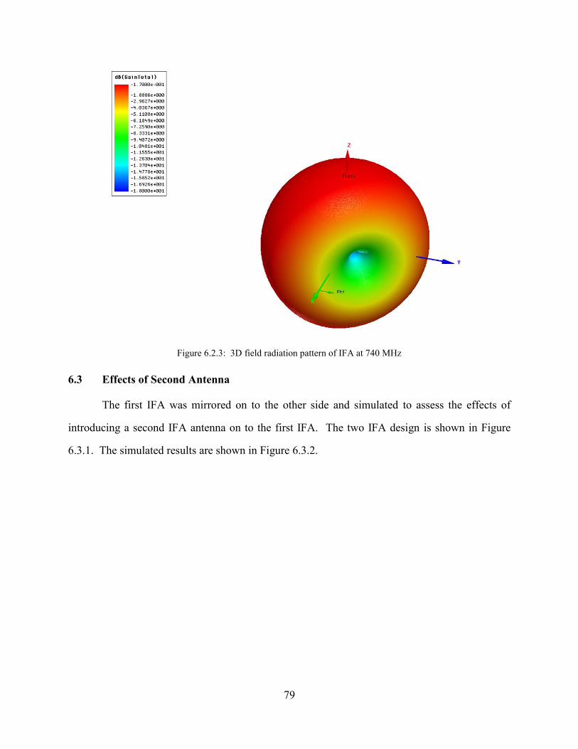
79
Figure 6.2.3: 3D field radiation pattern of IFA at 740 MHz
6.3 Effects of Second Antenna
The first IFA was mirrored on to the other side and simulated to assess the effects of
introducing a second IFA antenna on to the first IFA. The two IFA design is shown in Figure
6.3.1. The simulated results are shown in Figure 6.3.2.
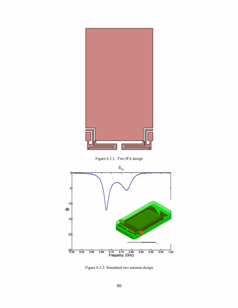
80
Figure 6.3.1: Two IFA design
Figure 6.3.2: Simulated two antenna design
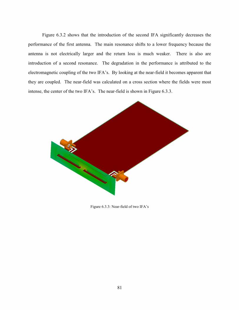
81
Figure 6.3.2 shows that the introduction of the second IFA significantly decreases the
performance of the first antenna. The main resonance shifts to a lower frequency because the
antenna is not electrically larger and the return loss is much weaker. There is also are
introduction of a second resonance. The degradation in the performance is attributed to the
electromagnetic coupling of the two IFA’s. By looking at the near-field it becomes apparent that
they are coupled. The near-field was calculated on a cross section where the fields were most
intense, the center of the two IFA’s. The near-field is shown in Figure 6.3.3.
Figure 6.3.3: Near-field of two IFA’s
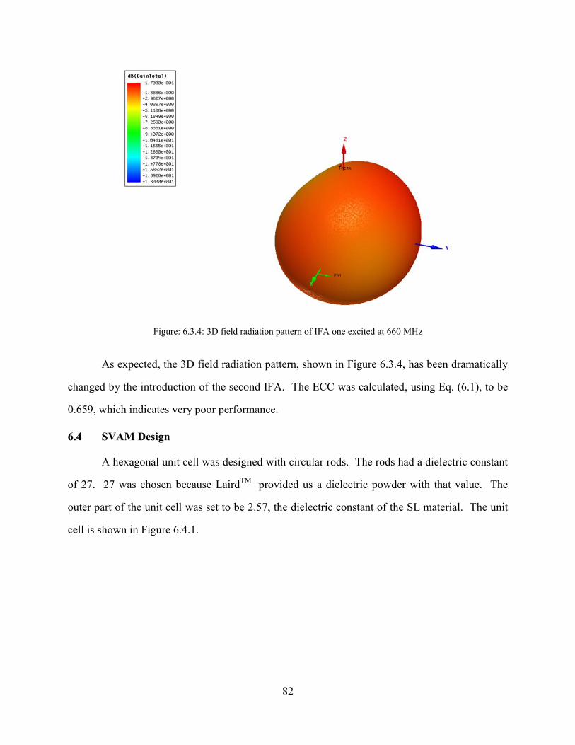
82
Figure: 6.3.4: 3D field radiation pattern of IFA one excited at 660 MHz
As expected, the 3D field radiation pattern, shown in Figure 6.3.4, has been dramatically
changed by the introduction of the second IFA. The ECC was calculated, using Eq. (6.1), to be
0.659, which indicates very poor performance.
6.4 SVAM Design
A hexagonal unit cell was designed with circular rods. The rods had a dielectric constant
of 27. 27 was chosen because LairdTM
provided us a dielectric powder with that value. The
outer part of the unit cell was set to be 2.57, the dielectric constant of the SL material. The unit
cell is shown in Figure 6.4.1.
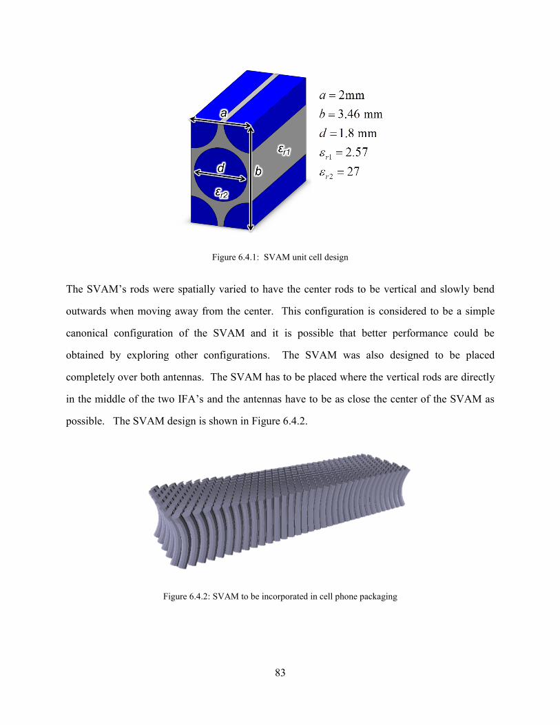
83
Figure 6.4.1: SVAM unit cell design
The SVAM’s rods were spatially varied to have the center rods to be vertical and slowly bend
outwards when moving away from the center. This configuration is considered to be a simple
canonical configuration of the SVAM and it is possible that better performance could be
obtained by exploring other configurations. The SVAM was also designed to be placed
completely over both antennas. The SVAM has to be placed where the vertical rods are directly
in the middle of the two IFA’s and the antennas have to be as close the center of the SVAM as
possible. The SVAM design is shown in Figure 6.4.2.
Figure 6.4.2: SVAM to be incorporated in cell phone packaging
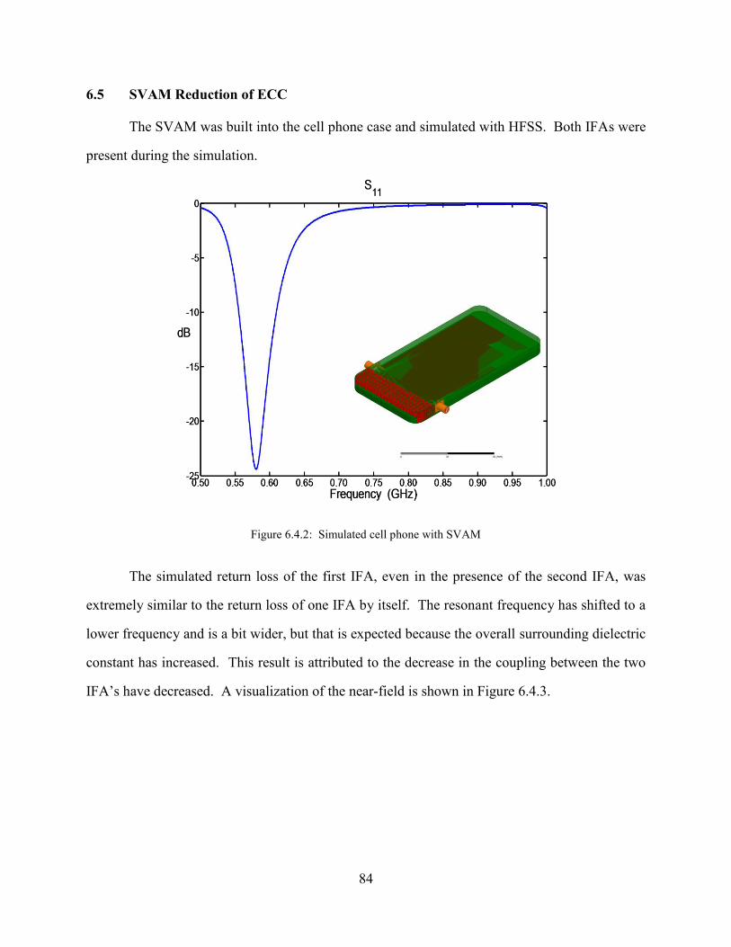
84
6.5 SVAM Reduction of ECC
The SVAM was built into the cell phone case and simulated with HFSS. Both IFAs were
present during the simulation.
Figure 6.4.2: Simulated cell phone with SVAM
The simulated return loss of the first IFA, even in the presence of the second IFA, was
extremely similar to the return loss of one IFA by itself. The resonant frequency has shifted to a
lower frequency and is a bit wider, but that is expected because the overall surrounding dielectric
constant has increased. This result is attributed to the decrease in the coupling between the two
IFA’s have decreased. A visualization of the near-field is shown in Figure 6.4.3.

85
Figure 6.4.3: Near-field of two IFA’s embedded in a SVAM
It is obvious from Figure 6.4.3 that the two IFA’s are no longer coupled. There are
discontinuities in the near field because the dielectric rods are a bit too large for the operating
frequency. This particular hole size was used because it is at the limit of what SL can print. The
ECC was calculated to be 0.01 using Eq. (6.1).
6.6 Conclusions
A SVAM was successfully designed to be incorporated into the packaging of a cell
phone. It was shown through simulation to dramatically improve the ECC of two cell phone
antennas in close proximity. The reduction in ECC can lead to denser packaging, smaller size,
and more functions. The results are summarizes in Table 6.6.1.
Table 6.6.1: ECC
Condition ECC
Two Antennas 0.659
Two antennas with SVAM 0.013
The ECC reduction, using the designed SVAM, yielded incredible results.
86
Chapter 7: Conclusions
7.1 Conclusions
The work shown in this dissertation demonstrates that 3D printed all-dielectric spatially
variant metamaterials (SVAM’s) can be used to mitigate the problems that arise when designing
fully 3D devices. All custom numerical tools used were formulated in this dissertation.
First, an all-dielectric uniaxial anisotropic metamaterial was successfully designed,
fabricated, and tested. It was manufactured from polycarbonate using a form of 3D printing
called fused deposition modeling. The full dielectric tensor was measured in the lab and the
experimental results corresponded well to the measured results.
Next, for the first time, an SVAM was used as means to sculpt the near-field around
devices. To begin this study, a simple but powerful technique to study transmission lines
embedded in spatially variant anisotropic media was outlined. This model was used to show that
the near-field can be sculpted almost arbitrarily with minimal change to the properties of the
device itself. This conclusion was confirmed with a rigorous 3D model. Based on these results,
a microstrip transmission line was isolated from a metal ball placed in close proximity by
embedding the line in a SVAM. The presence of the SVAM virtually eliminated any
interference of the ball on the microstrip, confirming this novel concept of managing fields in 3D
printed systems
Next, to evaluate the impact of surface roughness resulting from 3D printing of metals,
two Ku-band horn antennas were 3D printed using EBM. No post-processing steps were taken
to polish or otherwise improve the surface finish, which was measured to be on the order of 20 to
40 microns. The antennas were experimentally tested and compared to a standard horn antenna
purchased from Pasternack. It was observed that the surface roughness of horn #1
(25.9 μm RMS) had no measurable effect on the performance. Horn #2 had almost twice the
surface roughness (39.7 μm RMS) and we measured a 1 dB loss.
Finally, a SVAM was designed to dramatically enhance the performance of cell phone
antennas in close proximity. When two cell phone antennas were placed in close proximity the

87
ECC was 0.659. Then an SVAM was designed to be built into the case of the cell phone that
decreased the ECC to 0.01. The cell phone system can be full 3D printed.
7.2 Suggestion for Future Work
The design for the fully 3D printed cell phone is ready to be printed and experimentally
verified. The design is shown in Figure 7.2.1.
Figure 7.2.1: Cell phone with SVAM design
The SVAM was made to cover the entire area of the antennas. The SVAM could be optimized
to only be placed in the necessary location to achieve the same behavior. This leaves more space
for additional components or to accommodate smaller size.
All the devices designed in this dissertation used simple canonical configurations for the
anisotropy. . Future work could focus on developing a design methodology to improve the
technology even more. One possible methodology is the hybridization of TO and the SVL tool.
TO only calculates material properties, whereas the SVL tool calculates the actual
geometry that can be directly fabricated. From this perspective, hybridizing the two methods
will provide a single tool that can generate a device’s geometry directly from a spatial map of the
electromagnetic fields. Additional information needed to accomplish this includes lookup tables
that quantify the effective properties of different metamaterial unit cells as a function of their
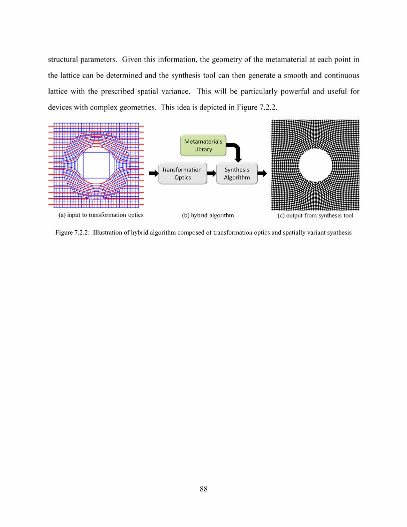
88
structural parameters. Given this information, the geometry of the metamaterial at each point in
the lattice can be determined and the synthesis tool can then generate a smooth and continuous
lattice with the prescribed spatial variance. This will be particularly powerful and useful for
devices with complex geometries. This idea is depicted in Figure 7.2.2.
Figure 7.2.2: Illustration of hybrid algorithm composed of transformation optics and spatially variant synthesis
89
References
[1] I. Gibson, D. W. Rosen, and B. Stucker, Additive manufacturing technologies: Springer,
2010.
[2] L. B. Gravelle and P. F. Wilson, "EMI/EMC in printed circuit boards-a literature review,"
Electromagnetic Compatibility, IEEE Transactions on, vol. 34, pp. 109-116, 1992.
[3] D. A. Hill, K. H. Cavcey, and R. T. Johnk, "Crosstalk between microstrip transmission
lines," Electromagnetic Compatibility, IEEE Transactions on, vol. 36, pp. 314-321, 1994.
[4] J. Isaacs Jr and N. Strakhov, "Crosstalk in uniformly coupled lossy transmission lines,"
Bell Syst. Tech. J, vol. 52, pp. 101-115, 1973.
[5] F. Xiao, W. Liu, and Y. Kami, "Analysis of crosstalk between finite-length microstrip
lines: FDTD approach and circuit-concept modeling," Electromagnetic Compatibility,
IEEE Transactions on, vol. 43, pp. 573-578, 2001.
[6] J.-P. Kruth, M. Leu, and T. Nakagawa, "Progress in additive manufacturing and rapid
prototyping," CIRP Annals-Manufacturing Technology, vol. 47, pp. 525-540, 1998.
[7] G. N. Levy, R. Schindel, and J.-P. Kruth, "Rapid manufacturing and rapid tooling with
layer manufacturing (LM) technologies, state of the art and future perspectives," CIRP
Annals-Manufacturing Technology, vol. 52, pp. 589-609, 2003.
[8] CustomPartNet. (4/16/14). Fused Deposition Modeling (FDM). Available:
http://www.custompartnet.com/wu/fused-deposition-modeling
[9] CustomPartNet. (4/16/2014). Stereolithography. Available:
http://www.custompartnet.com/wu/stereolithography
[10] D. Cormier, O. Harrysson, and H. West, "Characterization of H13 steel produced via
electron beam melting," Rapid Prototyping Journal, vol. 10, pp. 35-41, 2004.
[11] thre3d.com. How Electron Beam Melting (EBM) Works. Available:
https://thre3d.com/how-it-works/powder-bed-fusion/electron-beam-melting-ebm
[12] R. C. Rumpf, "Computational Electromagnetics (CEM): Lecture Series," ed: University
of Texas at El Paso, 2011.
[13] A. Sihvola, "Metamaterials in electromagnetics," Metamaterials, vol. 1, pp. 2-11, 2007.
[14] N. Engheta, "Circuits with light at nanoscales: optical nanocircuits inspired by
metamaterials," Science, vol. 317, pp. 1698-1702, 2007.
[15] C. Caloz and T. Itoh, "Novel microwave devices and structures based on the transmission
line approach of meta-materials," in Microwave Symposium Digest, 2003 IEEE MTT-S
International, 2003, pp. 195-198.
[16] D. Smith, J. Pendry, and M. Wiltshire, "Metamaterials and negative refractive index,"
Science, vol. 305, pp. 788-792, 2004.
[17] J. H. Kim and D. C. Park, "A simple method of crosstalk reduction by metal filled via
hole fence in bent transmission lines on PCBs," in Electromagnetic Compatibility, 2006.
EMC-Zurich 2006. 17th International Zurich Symposium on, 2006, pp. 363-366.
[18] G. E. Ponchak, D. Chun, J.-G. Yook, and L. P. Katehi, "Experimental verification of the
use of metal filled via hole fences for crosstalk control of microstrip lines in LTCC
packages," Advanced Packaging, IEEE Transactions on, vol. 24, pp. 76-80, 2001.
[19] R. Y. Sharma, T. Chakravarty, and A. B. Bhattacharyya, "Transient Analysis of
Microstrip–Like Interconnections Guarded by Ground Tracks," Progress In
Electromagnetics Research, vol. 82, pp. 189-202, 2008.
90
[20] A. R. Mallahzadeh, A. Ghasemi, S. Akhlaghi, B. Rahmati, and R. Bayderkhani,
"Crosstalk reduction using step shaped transmission line," Progress In Electromagnetics
Research C, vol. 12, pp. 139-148, 2010.
[21] J. H. Wu, J. Scholvin, J. A. del Alamo, and K. A. Jenkins, "A Faraday cage isolation
structure for substrate crosstalk suppression," Microwave and Wireless Components
Letters, IEEE, vol. 11, pp. 410-412, 2001.
[22] M. Karaboikis, C. Soras, G. Tsachtsiris, and V. Makios, "Compact dual-printed inverted-
F antenna diversity systems for portable wireless devices," Antennas and Wireless
Propagation Letters, IEEE, vol. 3, pp. 9-14, 2004.
[23] M. K. T. Al-Nuaimi and W. G. Whittow, "Performance investigation of a dual element
IFA array at 3 GHz for MIMO terminals," in Antennas and Propagation Conference
(LAPC), 2011 Loughborough, 2011, pp. 1-5.
[24] A. Lhilali, A. Diallo, C. Luxey, and P. Brachat, "Multiband multi-antenna system for
MIMO WLAN box," in Antenna Technology and Applied Electromagnetics & the
American Electromagnetics Conference (ANTEM-AMEREM), 2010 14th International
Symposium on, 2010, pp. 1-4.
[25] S. Zhang, A. A. Glazunov, Z. Ying, and S. He, "Reduction of the envelope correlation
coefficient with improved total efficiency for mobile LTE MIMO antenna arrays: Mutual
scattering mode," IEEE transactions on antennas and propagation, vol. 61, pp. 3280-
3291, 2013.
[26] C. Votis, G. Tatsis, and P. Kostarakis, "Envelope Correlation Parameter Measurements in
a MIMO Antenna Array Configuration," Engineering, vol. 2, 2010.
[27] Ansys. Ansys HFSS. Available:
http://www.ansys.com/Products/Simulation+Technology/Electronics/Signal+Integrity/A
NSYS+HFSS
[28] D. W. Berreman, "Optics in stratified and anisotropic media: 4× 4-matrix formulation,"
JOSA, vol. 62, pp. 502-510, 1972.
[29] R. Azzam, "Propagation of partially polarized light through anisotropic media with or
without depolarization: a differential 4× 4 matrix calculus," JOSA, vol. 68, pp. 1756-
1767, 1978.
[30] P. Karasinski, "Application of the 4x4 matrix method for the modeling of planar
waveguide sensors," in Lightguides and their Applications, 2000, pp. 229-234.
[31] P. Lin-Chung and S. Teitler, "4x4 Matrix formalisms for optics in stratified anisotropic
media," JOSA A, vol. 1, pp. 703-705, 1984.
[32] N. J. Higham, Functions of matrices: theory and computation: Siam, 2008.
[33] R. Redheffer, "Difference equations and functional equations in transmission-line
theory," Modern mathematics for the engineer, vol. 12, pp. 282-337, 1961.
[34] S. Guo and S. Albin, "Simple plane wave implementation for photonic crystal
calculations," Optics Express, vol. 11, pp. 167-175, 2003.
[35] S. Johnson and J. Joannopoulos, "Block-iterative frequency-domain methods for
Maxwell's equations in a planewave basis," Optics Express, vol. 8, pp. 173-190, 2001.
[36] K. Leung and Y. Liu, "Photon band structures: The plane-wave method," Physical
Review B, vol. 41, p. 10188, 1990.
[37] R. Meade, A. Rappe, K. Brommer, J. Joannopoulos, and O. Alherhand, "Erratum:
Accurate theoretical analysis of photonic band-gap materials (Phys. Rev. B 48, 8434
(1993))," Physical Review-Section B-Condensed Matter, vol. 55, p. 15942, 1997.
91
[38] S. Shi, C. Chen, and D. W. Prather, "Plane-wave expansion method for calculating band
structure of photonic crystal slabs with perfectly matched layers," JOSA A, vol. 21, pp.
1769-1775, 2004.
[39] H. Sözüer and J. P. Dowling, "Photonic band calculations for woodpile structures,"
Journal of Modern Optics, vol. 41, pp. 231-239, 1994.
[40] R. C. Rumpf, "Design and optimization of nano-optical elements by coupling fabrication
to optical behavior," University of Central Florida Orlando, Florida, 2006.
[41] R. C. Rumpf, C. R. Garcia, H. H. Tsang, J. E. Padilla, and M. D. Irwin, "Electromagnetic
Isolation of A Microstrip by Embedding in a Spatially Variant Anisotropic
Metamaterial," Progress In Electromagnetics Research, vol. 142, 2013.
[42] S. Y. Poh, W. C. Chew, and J. Kong, "Approximate formulas for line capacitance and
characteristic impedance of microstrip line," IEEE TRANS. MICROWAVE THEORY AND
TECH., vol. 29, pp. 135-142, 1981.
[43] R. C. Rumpf, "Simple implementation of arbitrarily shaped total-field/scattered-field
regions in fnite-difference frequency-domain," Progress In Electromagnetics Research B,
vol. 36, 2012.
[44] S. Boonruang, A. Greenwell, and M. Moharam, "Multiline two-dimensional guided-mode
resonant filters," Applied optics, vol. 45, pp. 5740-5747, 2006.
[45] K. S. Yee, "Numerical solution of initial boundary value problems involving Maxwell’s
equations," IEEE Trans. Antennas Propag, vol. 14, pp. 302-307, 1966.
[46] J. H. Barton, R. C. Rumpf, R. W. Smith, C. Kozikowski, and P. Zellner, "ALL-
DIELECTRIC FREQUENCY SELECTIVE SURFACES WITH FEW NUMBER OF
PERIODS," Progress In Electromagnetics Research B, vol. 41, 2012.
[47] A. J. Pung, S. R. Carl, I. R. Srimathi, and E. G. Johnson, "Method of fabrication for
encapsulated polarizing resonant gratings," Photonics Technology Letters, IEEE, vol. 25,
pp. 1432-1434, 2013.
[48] R. C. Rumpf and J. Pazos, "Synthesis of spatially variant lattices," Optics express, vol.
20, pp. 15263-15274, 2012.
[49] J. B. Pendry, D. Schurig, and D. R. Smith, "Controlling electromagnetic fields," science,
vol. 312, pp. 1780-1782, 2006.
[50] D.-H. Kwon and D. H. Werner, "Transformation optical designs for wave collimators,
flat lenses and right-angle bends," New Journal of Physics, vol. 10, p. 115023, 2008.
[51] D. Schurig, J. Mock, B. Justice, S. A. Cummer, J. Pendry, A. Starr, et al., "Metamaterial
electromagnetic cloak at microwave frequencies," Science, vol. 314, pp. 977-980, 2006.
[52] W. Cai, U. K. Chettiar, A. V. Kildishev, and V. M. Shalaev, "Optical cloaking with
metamaterials," Nature photonics, vol. 1, pp. 224-227, 2007.
[53] S. Datta, C. Chan, K. Ho, and C. Soukoulis, "Effective dielectric constant of periodic
composite structures," Physical Review B, vol. 48, p. 14936, 1993.
[54] A. Krokhin, P. Halevi, and J. Arriaga, "Long-wavelength limit (homogenization) for two-
dimensional photonic crystals," Physical Review B, vol. 65, p. 115208, 2002.
[55] A. Nicolson and G. Ross, "Measurement of the intrinsic properties of materials by time-
domain techniques," Instrumentation and Measurement, IEEE Transactions on, vol. 19,
pp. 377-382, 1970.
[56] G. A. Niklasson, C. Granqvist, and O. Hunderi, "Effective medium models for the optical
properties of inhomogeneous materials," Applied Optics, vol. 20, pp. 26-30, 1981.
92
[57] H. M. Jaeger and S. R. Nagel, "Physics of the granular state," Science, vol. 255, pp. 1523-
1531, 1992.
[58] D. Aspnes, "Local-field effects and effective-medium theory: A microscopic
perspective," Am. J. Phys, vol. 50, 1982.
[59] S. Gaytan, L. Murr, E. Martinez, J. Martinez, B. Machado, D. Ramirez, et al.,
"Comparison of microstructures and mechanical properties for solid and mesh cobalt-
base alloy prototypes fabricated by electron beam melting," Metallurgical and Materials
Transactions A, vol. 41, pp. 3216-3227, 2010.
[60] L. Murr, S. Gaytan, A. Ceylan, E. Martinez, J. Martinez, D. Hernandez, et al.,
"Characterization of titanium aluminide alloy components fabricated by additive
manufacturing using electron beam melting," Acta Materialia, vol. 58, pp. 1887-1894,
2010.
[61] J. Parthasarathy, B. Starly, S. Raman, and A. Christensen, "Mechanical evaluation of
porous titanium (Ti6Al4V) structures with electron beam melting (EBM)," Journal of the
mechanical behavior of biomedical materials, vol. 3, pp. 249-259, 2010.
[62] A. Gebhardt, F.-M. Schmidt, J.-S. Hötter, W. Sokalla, and P. Sokalla, "Additive
manufacturing by selective laser melting the realizer desktop machine and its application
for the dental industry," Physics Procedia, vol. 5, pp. 543-549, 2010.
[63] T. Pereira, M. Silva, M. Oliveira, I. Maia, J. Silva, M. Costa, et al., "Effect of process
parameters on the properties of selective laser sintered Poly (3-hydroxybutyrate)
scaffolds for bone tissue engineering," Virtual and Physical Prototyping, vol. 7, pp. 275-
285, 2012.
[64] C. L. Holloway and E. F. Kuester, "Power loss associated with conducting and
superconducting rough interfaces," Microwave Theory and Techniques, IEEE
Transactions on, vol. 48, pp. 1601-1610, 2000.
[65] Y. Ning and W. Jiang, "The electromagnetic characteristics of conducting rough surfaces
at millimeter wave frequencies," in Microwave and Millimeter Wave Technology, 2008.
ICMMT 2008. International Conference on, 2008, pp. 326-328.
[66] Y. Uehara, Y. Suzuki, H. Komagata, T. Tsuruoka, and S. Ushioda, "Electron Energy Loss
Spectra Showing the Effects of Surface Roughness and Electromagnetic Retardation---
Theory and Experiment," Journal of the Physical Society of Japan, vol. 70, p. 2012,
2001.
[67] N. Chiurtu, B. Rimoldi, I. Telatar, and V. Pauli, "Impact of correlation and coupling on
the capacity of MIMO systems," in Signal Processing and Information Technology,
2003. ISSPIT 2003. Proceedings of the 3rd IEEE International Symposium on, 2003, pp.
154-157.
[68] J. Thaysen and K. B. Jakobsen, "Envelope correlation in (N, N) MIMO antenna array
from scattering parameters," Microwave and optical technology letters, vol. 48, pp. 832-
834, 2006.
[69] R. G. Vaughan and J. B. Andersen, "Antenna diversity in mobile communications,"
Vehicular Technology, IEEE Transactions on, vol. 36, pp. 149-172, 1987.
[70] P. Panayi, M. Al-Nuaimi, and L. Ivrissimtzis, "Tuning techniques for the planar inverted-
F antenna," 1999.
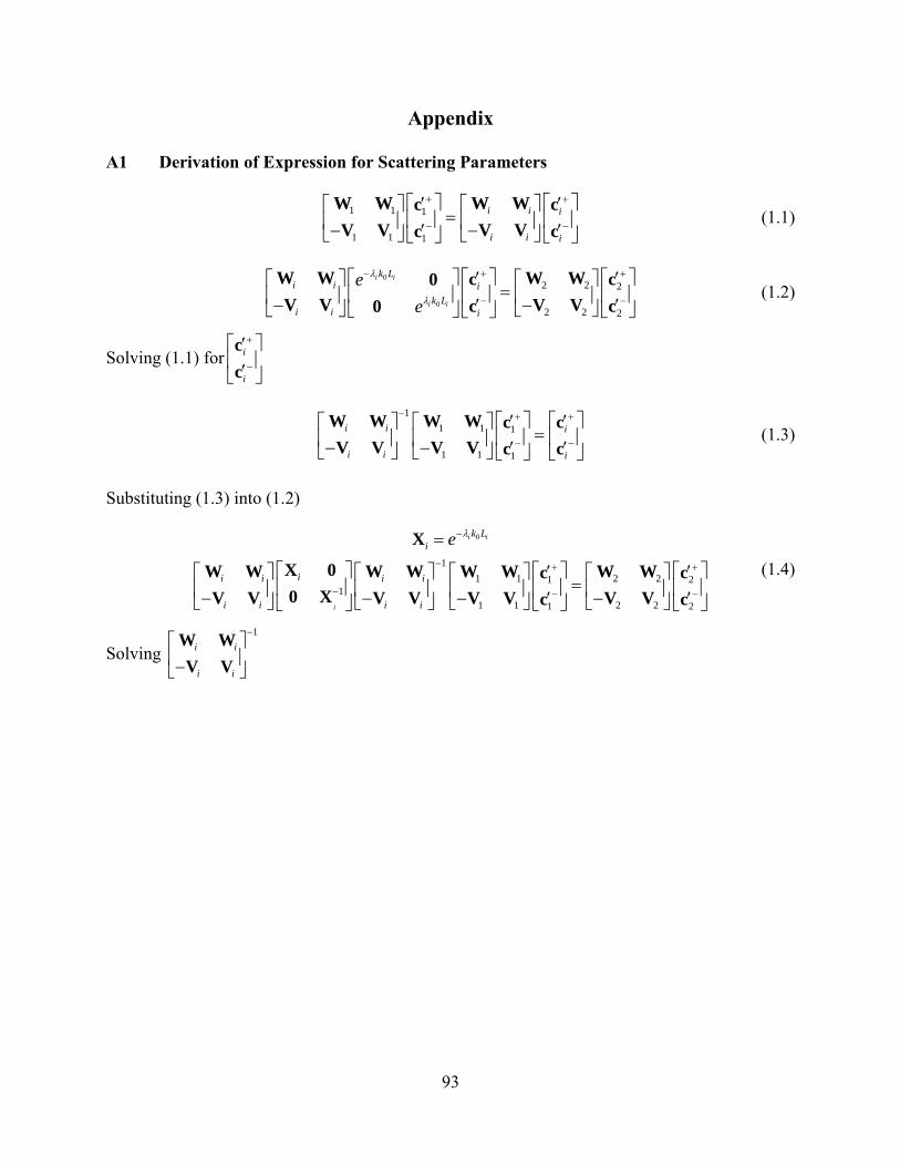
93
Appendix
A1 Derivation of Expression for Scattering Parameters
1 1 1
1 1 1
i i i
i i i
W WW W cc
V VV V cc (1.1)
0
0
2 2 2
2 2 2
i i
i i
k Li i i
k Li i i
e
e
W W W Wc c0
V V V Vc c0 (1.2)
Solving (1.1) fori
i
c
c
1
1 1 1
1 1 1
i i i
i i i
W W W W cc
V V V V cc (1.3)
Substituting (1.3) into (1.2)
0
1
1 1 2 21 2
1
1 1 2 21 2
i i
i
k L
i
ii i i i
i i i i
e
X
X 0W W W W W W W Wc c
0 XV V V V V V V Vc c
(1.4)
Solving
1
i i
i i
W W
V V
94
1
1
1
1
1 1 1
1
1 1
1 1 1
1 1
1 1
1 1
2
i
i
i
i
i i i
i
i i
i i i
i i
i i
i i
i i
i i
i i
i i
i
W W 1 0
V V 0 1
W 01 1
V V 0 1
W 01 1
0 V V W 1
W 01 1
V V W V0 1
2 2
W 01 1
W V0 1
2 2
2W W V
1 0 2 2 2
0 1 W V
2 2
W V
1 0 2 2
0 1 W V
2 21 1 1
1 1
1
2
i i i i
i i i i
W W W V
V V W V
(1.5)
Substituting (1.5) into (1.4)
95
1 1
1 1 2 21 21 1 1
1 1 2 21 2
1 11 1 21
1 1 11 1 1
1
2
1
2
i
i
ii i i i
i i i i
ii i i i
i i i i
X 0W W W W W WW V c c
0 XV V V V V VW V c c
X 0W W W W W WW V c
0 XV V V VW V c
2 2
2 2 2
1 12 21 1 1 1 2
1 1 12 21 1 1 1 2
1 1
1 1 1 1
1
1
2
1
2
i
i
ii i i i
i i i i
i i iii i
i i
c
V V c
X 0W W W WW V Wc Wc c
0 XV V V VW V Vc Vc c
W Wc W Wc VX 0W W
0 XV V
1 1
1 1 1 1 2 2 2
1 1 1 12 2 21 1 1 1 1 1 1 1
1 1 1 1
1 1 1 1 1 1 1 11 1 1
1 1 1 1
1
2i
i
i i i i
ii i i i i i
i i i i i
Vc V Vc W W c
V V cW Wc W Wc V Vc V Vc
X 0W W W Wc V Vc W Wc V Vc
0 XV V W Wc V Vc W
2 2 2
1 12 21 1 1 1 2
1 1 1 1 11 1 1 1 1 1 2 2 2
11 1 1 1
2 2 21 1 1 1 1 1
1
2i
i
i i i ii i i
i ii i i i
i
W W c
V VWc V Vc c
W W V V c W W V V cX 0 W W W W c
0 X V V V V cW W V V c W W V V c
X 0
0
1 12 2, 1 1 , 1 1 2
1 1 12 2, 1 1 , 1 1 2
1 1
, 1 1 , 1 1 2 2 2 2
1
, 1 1 , 1 1
1 1
2 2i
i
i i i i i i
i i i i i i
i i i i i i i
i i i i
W WA c B c W V c
X V VB c A c W V c
X 0 A c B c W W c W W c
0 X B c A c
1 1
2 2 2 2
1 1 1 1
2 2 2 2 2 2 2 2
1 1 1 1
2 2 2 2 2 2, 1 1 , 1 1
1 1 1 1 1 1, 1 1 , 1 1 2 2 2 2 2i i
i i
i i i i
i i i ii i i i i i
i i i i i i i i
V V c V V c
W W c W W c V V c V V c
W W V V c W W V V cX A c X B c
X B c X A c W W V V c W W V V 2
, 1 1 , 1 1 , 1 2 , 1 2
1 1
, 1 1 , 1 1 , 1 2 , 1 2
, 1 1 , 1 1 ,
, 1 1 , 1 1
i i
i i i i i i i i i i
i i i i i i i i i
i i i i i i i
i i i i
i
c
X A c X B c I 0I 0 A c B c
X B c X A c 0 X0 X B c A c
X A c X B c A
B c A c
1 2 , 1 2
, 1 2 , 1 2
i i i
i i i i i i
c B c
X B c X A c
(1.6)
Separating the last equation from (1.6)
, 1 1 , 1 1 , 1 2 , 1 2i i i i i i i i i i
X A c X B c A c B c (1.7)
, 1 1 , 1 1 , 1 2 , 1 2i i i i i i i i i i
B c A c X B c X A c (1.8)
Solving (1.8) for 1
c
, 1 , 1 , 1
1 1 1
1 , 1 1 , 1 2 , 1 2i i i i i ii i i i i i i i
c A B c A X B c A X A c (1.9)

96
Substituting (1.9) into (1.7)
, 1 , 1 , 1
1 1 1
, 1 1 , 1 , 1 1 , 1 , 1 2 , 1 , 1 2 , 1 2 , 1 2i i i i i ii i i i i i i i i i i i i i i i i i i i i i i i
X A c X B A B c X B A X B c X B A X A c A c B c (1.10)
Solving (1.10) for 2
c
, 1 , 1 , 1
, 1 , 1
1 1 1
, 1 , 1 2 , 1 2 , 1 , 1 1 , 1 1 , 1 , 1 2 , 1 2
1 1
, 1 , 1 , 1 2 , 1 , 1 , 1 1 , 1
i i i i i i
i i i i
i i i i i i i i i i i i i i i i i i i i i i i i
i i i i i i i i i i i i i i i i i i i
X B A X B c A c X B A B c X A c X B A X A c B c
A X B A X B c X A X B A B c X B A
, 1
, 1 , 1 , 1 , 1
1
, 1 , 1 2
1 11 1 1 1
2 , 1 , 1 , 1 , 1 , 1 , 1 1 , 1 , 1 , 1 , 1 , 1 , 1 2
i i
i i i i i i i i
i i i i i
i i i i i i i i i i i i i i i i i i i i i i i i i i i i i i i i
X A B c
c A X B A X B X A X B A B c A X B A X B X B A X A B c
(1.11)
Solving (1.7) for 2
c
, 1 , 1 , 1
1 1 1
2 , 1 1 , 1 1 , 1 2i i i i i ii i i i i i i i
c A X A c A X B c A B c (1.12)
Substituting (1.12) into (1.8)
, 1 , 1 , 1
1 1 1
, 1 1 , 1 1 , 1 , 1 1 , 1 , 1 1 , 1 , 1 2 , 1 2i i i i i ii i i i i i i i i i i i i i i i i i i i i i i i
B c A c X B A X A c X B A X B c X B A B c X A c (1.13)
Solving (1.13) for 1
c
, 1 , 1 , 1
, 1 , 1
1 1 1
, 1 1 , 1 , 1 1 , 1 , 1 1 , 1 1 , 1 , 1 2 , 1 2
1 1
, 1 , 1 , 1 1 , 1 , 1 , 1 1 , 1
i i i i i i
i i i i
i i i i i i i i i i i i i i i i i i i i i i i i
i i i i i i i i i i i i i i i i i i i
A c X B A X B c X B A X A c B c X B A B c X A c
A X B A X B c X B A X A B c X A
, 1
, 1 , 1 , 1 , 1
1
, 1 , 1 2
1 11 1 1 1
1 , 1 , 1 , 1 , 1 , 1 , 1 1 , 1 , 1 , 1 , 1 , 1 , 1 2
i i
i i i i i i i i
i i i i i
i i i i i i i i i i i i i i i i i i i i i i i i i i i i i i i i
X B A B c
c A X B A X B X B A X A B c A X B A X B X A X B A B c
(1.14)
Putting (1.11) and (1.14) together
, 1 , 1 , 1 , 1
, 1 , 1
1 11 1 1 1
, 1 , 1 , 1 , 1 , 1 , 1 , 1 , 1 , 1 , 1 , 1 , 11
11 12
, 1 , 1 , 1 , 1 , 1 ,
i i i i i i i i
i i i i
i i i i i i i i i i i i i i i i i i i i i i i i i i i i i i i
i i i i i i i i i i i i i i
A X B A X B X B A X A B A X B A X B X A B A Bc
cA X B A X B X A B A B
, 1 , 1
1
11 1 2
1 , 1 , 1 , 1 , 1 , 1 , 1i i i ii i i i i i i i i i i i i i i i i
c
cA X B A X B X B A X A B
(1.15)
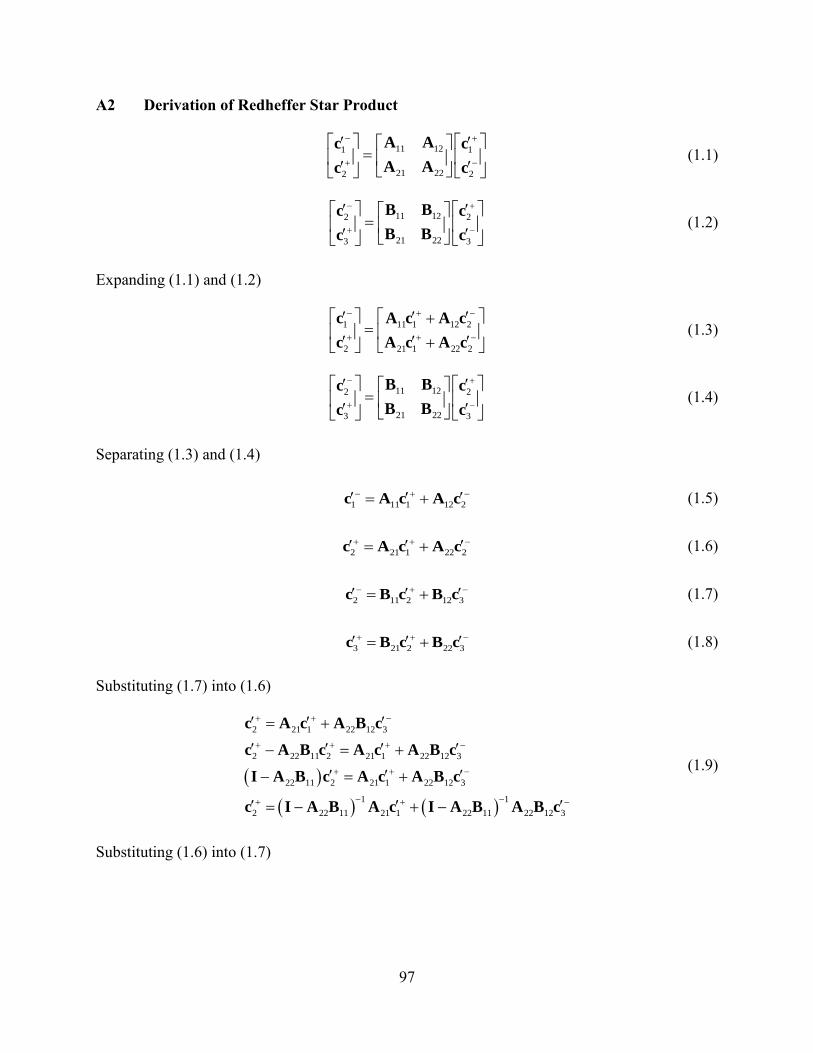
97
A2 Derivation of Redheffer Star Product
11 121 1
21 222 2
A Ac c
A Ac c (1.1)
11 122 2
21 223 3
B Bc c
B Bc c (1.2)
Expanding (1.1) and (1.2)
1 11 1 12 2
2 21 1 22 2
c A c A c
c A c A c (1.3)
11 122 2
21 223 3
B Bc c
B Bc c (1.4)
Separating (1.3) and (1.4)
1 11 1 12 2
c A c A c (1.5)
2 21 1 22 2
c A c A c (1.6)
2 11 2 12 3
c B c B c (1.7)
3 21 2 22 3
c B c B c (1.8)
Substituting (1.7) into (1.6)
2 21 1 22 12 3
2 22 11 2 21 1 22 12 3
22 11 2 21 1 22 12 3
1 1
2 22 11 21 1 22 11 22 12 3
c A c A B c
c A B c A c A B c
I A B c A c A B c
c I A B A c I A B A B c
(1.9)
Substituting (1.6) into (1.7)

98
2 11 21 1 11 22 2 12 3
2 11 22 2 11 21 1 12 3
11 22 2 11 21 1 12 3
1 1
2 11 22 11 21 1 11 22 12 3
c B A c B A c B c
c B A c B A c B c
I B A c B A c B c
c I B A B A c I B A B c
(1.10)
Substituting (1.9) into (1.8)
1 1
3 21 22 11 21 1 21 22 11 22 12 3 22 3
1 1
3 21 22 11 21 1 21 22 11 22 12 22 3
c B I A B A c B I A B A B c B c
c B I A B A c B I A B A B B c (1.11)
Substituting (1.10) into (1.5)
1 1
1 11 1 12 11 22 11 21 1 12 11 22 12 3
1 1
1 11 12 11 22 11 21 1 12 11 22 12 3
c A c A I B A B A c A I B A B c
c A A I B A B A c A I B A B c (1.12)
Combining (1.11) and (1.12) into block matrix form
1 1
1 11 12 11 22 11 21 1 12 11 22 12 3
1 1
3 21 22 11 21 1 21 22 11 22 12 22 3
1 1
11 12 11 22 11 21 12 11 22 121
1 1
3 21 22 11 21 21 22 11 22 12 22
c A A I B A B A c A I B A B c
c B I A B A c B I A B A B B c
A A I B A B A A I B A Bc
c B I A B A B I A B A B B
1
3
c
c
(1.13)
99
Vita
Cesar R. Garcia earned his Bachelors of Science in Engineering Physics from The
University of Texas at Brownsville in 2009. During his undergraduate he started working in
applied electromagnetics at the Applied Microwave & Electromagnetic Laboratory (AMEL). He
developed a novel negative index metamaterial and used it to miniaturize a patch antenna. This
work gave him the opportunity to be the only undergraduate to present at the "iWAT 2009 :
IEEE International Workshop on Antenna Technology - Small Antennas and Novel
Metamaterials". After graduating, he spent the summer working as a summer provost intern,
under Dr. Ruyan Guo at the Multifunction Electronic Materials Devices Research Lab
(MeMDRL) located at The University of Texas at San Antonio. He worked on simulating the
effect of a piezoelectric on an impinging electromagnetic wave. That work led to another peer
reviewed publication
Dr. Garcia research is focused on 3D printed electromagnetics. He developed and
demonstrated the world's first spatially variant anisotropic metamaterial to sculpt the fields
around devices like they are clay. He is using this to isolate electromagnetic components placed
in close proximity and to enhance the performance of components forced into awkward form
factors. Dr. Garcia developed and tested the world's first 3D printed horn antenna to show that
surface roughness can be tolerated. He assisted in the design and demonstration of the world's
first spatially variant self-collimating photonic crystal that the team is using to control the flow
of waves in all three dimensions. This work is now being implemented at the nano-scale for
integrated optical devices. Dr. Garcia is an author on four peer-reviewed journal articles, two as
first author, and has more publications pending. He was also a winner of the prestigious NSF
Louis Stokes Alliance for Minority Participation Bridge to Doctorate Fellowship.
Dr. Garcia plans on working in industry. After serving some tenure in industry, he plans
to return to academia and start his own research group in the area of applied electromagnetics.

100
Permanent address: 9375 Viscount BLVD Apt 2014
El Paso, TX, 79925
This dissertation was typed by the author.