28 de febrero y 5 y 6 de marzo 2012 - webs.ucm.eswebs.ucm.es/info/giboucm/images/ml_calvo/5 6...
72
Guías de onda óptica 28 de febrero y 5 y 6 de marzo 2012 Prof. María L. Calvo
Transcript of 28 de febrero y 5 y 6 de marzo 2012 - webs.ucm.eswebs.ucm.es/info/giboucm/images/ml_calvo/5 6...

Guías de onda óptica
28 de febrero y 5 y 6 de marzo 2012
Prof. María L. Calvo

PROPAGACION DEL CAMPO ELECTROMAGNETICO EN
UN DIELECTRICO ISOTROPO HOMOGENEO• ECUACIONES DE MAXWELL:
• 1.-
• 2.-
• 3.-
• 4.-
0; 0; 0; 0D E E E
; HEc t
0; 0; =0B H H H
; =0; 0;EH j Ec t

Aplicando el operador rotacional en la ec.(2) y teniendo en cuenta que el medio no tiene propiedades magnéticas:
• De acuerdo con la ec.(4):
1E Hc t
2
2 2
1 EEc t c t
t
EEc t

Aplicando relaciones de análisis vectorial:
• Puesto que:
• Obtenemos:
2E E E
0E
22
2 2 0EEc t
ecuación diferencial de ondas para la propagación del campo electromagnético en un medio isótropo, dieléctrico, homogéneoy no dispersivo

SOLUCION A LA ECUACION DE ONDAS:
• Onda plana monocromática armónica en el tiempo:
, exp
: amplitud onda incidente
2, , ;
o
o
x y z
E r t E i kr wt
E
k k k k k

Derivando respecto del tiempo:
Sustituyendo en la ec. diferencial de ondas
• Se cumple además:
• Por tanto: ecuación diferencial de ondas para el c.e.m. propagándose en un medio isótropo, dieléctrico y homogéneo en forma de onda plana monocromática y armónica con k=2/
22
2
E Et
22
2 0
; modulo del vector de onda en el vacioo
E Ec
kc
2o
2
; por ser un dielectrico:
; permitividad dielectrica relativa al vacio
o o
ro
n
n
2
22 22r r o ok nk k
c
2 2 0k E 2 2 0k E

PROPAGACIÓN DEL C.E.M. EN UN MEDIO DIELÉCTRICO ISÓTROPO E
INHOMOGÉNEO• En este caso:
• Por tanto:
0; 0; 0D E E
22
2 2
22
2 2
0; ln
ln 0
EE Ec t
E E E E E
EE Ec t

Condición de medio inhomogéneo transversal:
• Suponemos:
• El operador laplaciana solo actúa sobre coordenadas (x,y).
• Definimos:
,x y
2 22
2 2 : operador transversalx y
Se obtiene otra forma de ecuación diferencial:
2
22 2
1ln , , 0EE E x y x yc t
22
2 2
1ln , , 0EE E x y x yc t
Para determinada.

SOLUCION:• Para simplificar se impone una solución de tipo onda plana
monocromática armónica en el tiempo.
, , ,E E r t E r z t
• Descomposición modal del campo:El c.e.m. propagado en una guía de ondas sólo soporta un número finitode modos de propagación confinados:
, , , , , , , ,j j radj j
j j
E r z t a E r z t a E r z t E r z t con: j = 1,2,....M : índice modal.Y análogamente para el campo magnético.
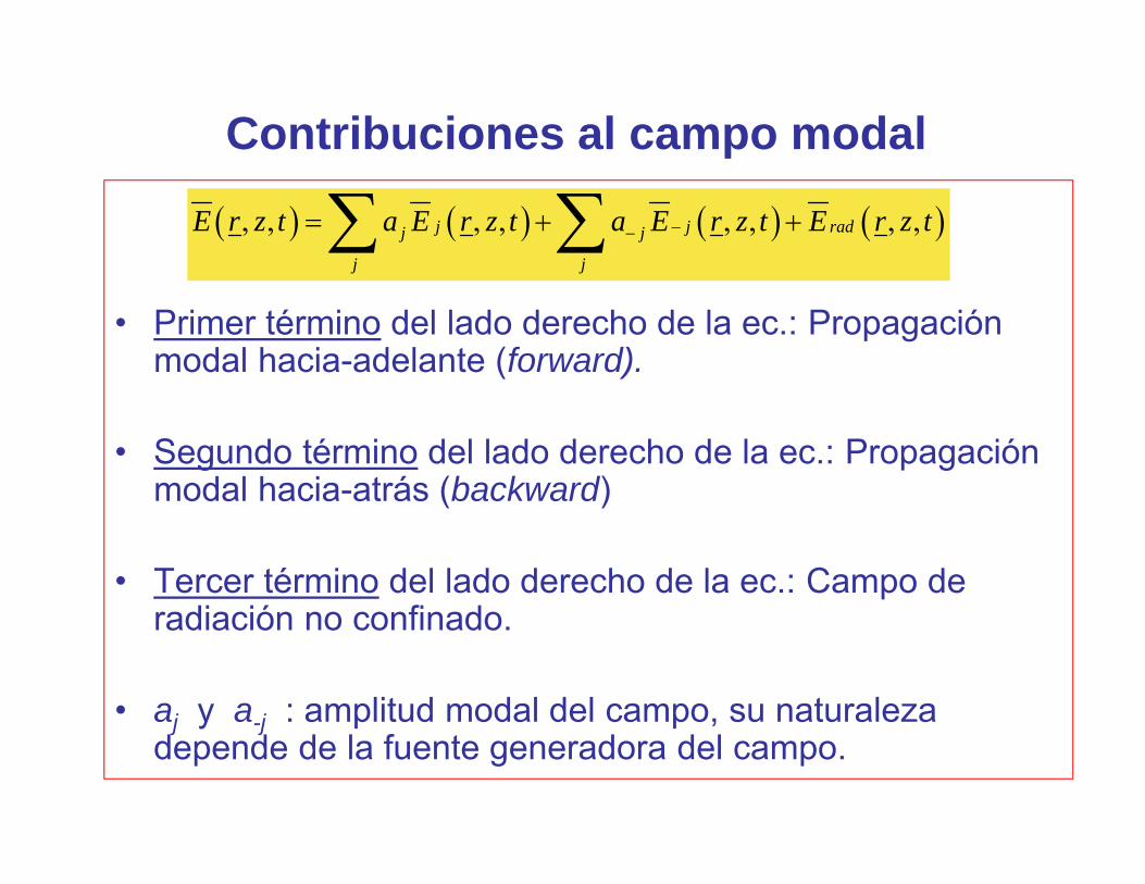
Contribuciones al campo modal
• Primer término del lado derecho de la ec.: Propagación modal hacia-adelante (forward).
• Segundo término del lado derecho de la ec.: Propagación modal hacia-atrás (backward)
• Tercer término del lado derecho de la ec.: Campo de radiación no confinado.
• aj y a-j : amplitud modal del campo, su naturaleza depende de la fuente generadora del campo.
, , , , , , , ,j j radj j
j j
E r z t a E r z t a E r z t E r z t

Supondremos, para cada campo modal :
, , exp
, 0
, 0
j oj z
j j
j j j
E r z E x y i z
a
a
• los valores de j se obtienen a partir de una ecuaciónde autovalores.
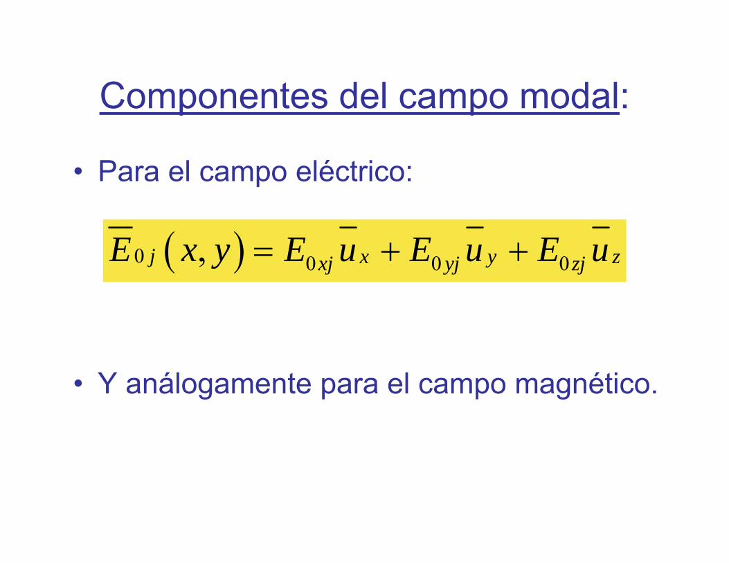
Componentes del campo modal:
• Para el campo eléctrico:
• Y análogamente para el campo magnético.
0 0 0 0,j x y zxj yj zjE x y E u E u E u

CASOS PARTICULARES:• Modos TE:• Supondremos: 0zjE
• Hay una simplificación en la ec. diferencial de ondas.• En particular, se anula el término que contiene ln.
• La condición se cumple en guías con simetría cilíndrica y en guías de onda planas.
• La ec. de diferencias de ondas es:
2 2 2 20 0jo jn k E
2 2 2 20 0jo jn k E
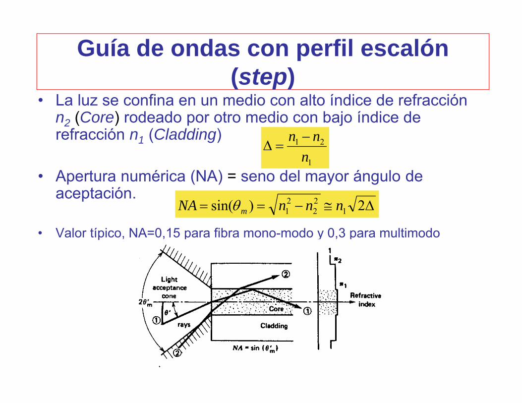
Guía de ondas con perfil escalón (step)
• La luz se confina en un medio con alto índice de refracción n2 (Core) rodeado por otro medio con bajo índice de refracción n1 (Cladding)
• Apertura numérica (NA) = seno del mayor ángulo de aceptación.
• Valor típico, NA=0,15 para fibra mono-modo y 0,3 para multimodo
2)sin( 122
21 nnnNA m
1
21
nnn

Guia escalón monomodo: Sección transversal
Protective polymerinc coating
Buffer tube: d = 1mm
Cladding: d = 125 - 150 m
Core: d = 8 - 10 mn
r
The cross section of a typical single-mode fiber with a tight buffertube. (d = diameter)
n1
n2
© 1999 S.O. Kasap, Optoelectronics (Prentice Hall)

Guía escalón multimodo
1
22
1
22
21 12 n
nn
nn

Reflexión total interna
Cladding
Corem ax
AB
< c
A
B
> c
m ax
n0 n1
n2
Lost
Propagates
Maximum acceptance anglemax is that which just givestotal internal reflection at thecore-cladding interface, i.e.when = max then = c.Rays with > max (e.g. rayB) become refracted andpenetrate the cladding and areventually lost.
Fiber axis
© 1999 S.O. Kasap, Optoelectronics (Prentice Hall)Formación de una onda evanescente.

Onda EvanescenteOnda electromagnética que se amortigua exponencialmente con la distancia desde la inter-fase de separación de los dos medios ópticos.
core cladding
Aplicaciones: Microscopía de efecto tunel.
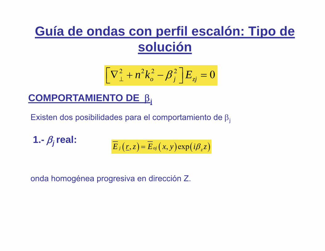
Guía de ondas con perfil escalón: Tipo de solución
2 2 2 2 0o j zjn k E
COMPORTAMIENTO DE j
Existen dos posibilidades para el comportamiento de j
1.- j real: , , expj oj zE r z E x y i z
onda homogénea progresiva en dirección Z.
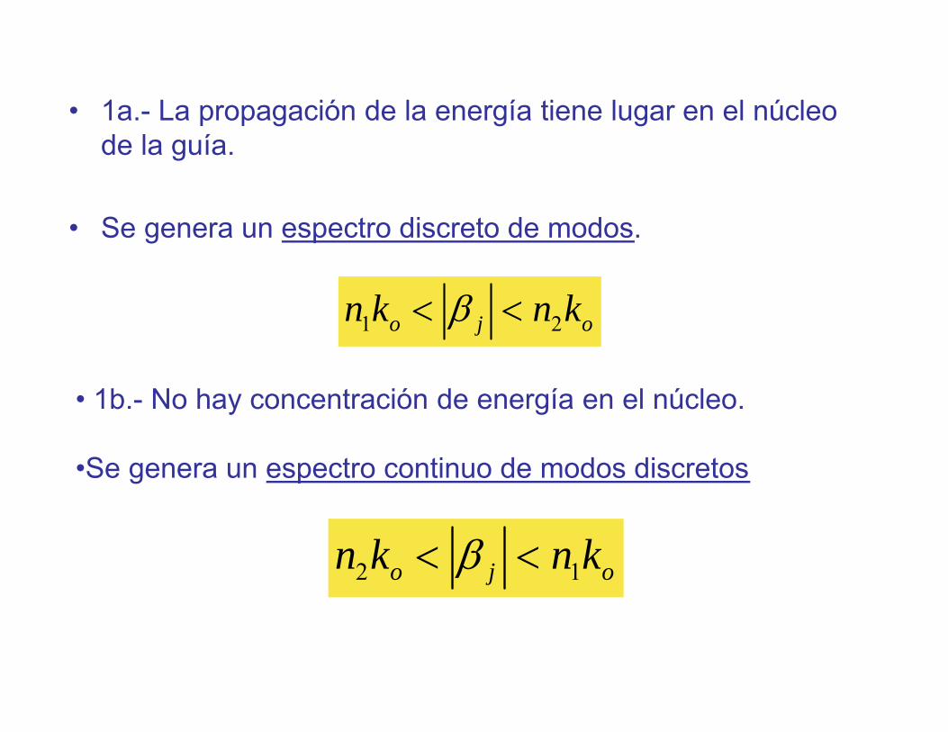
• 1a.- La propagación de la energía tiene lugar en el núcleo de la guía.
• Se genera un espectro discreto de modos.
1 2o j on k n k
• 1b.- No hay concentración de energía en el núcleo.
•Se genera un espectro continuo de modos discretos
2 1o j on k n k

2.- j compleja:
Re Imij j j
La componente espacial del campo modal es ahora(factorizamos t):
, exp Re exp Imj ojE r E x y i z zj j

Rango espectral de
+n1k0 +n2k0
Im
Re
Modos de radiación evanescentes
-n1k0 -n2k0
Modos guiados
Espectro discreto
Modos guiados
Espectro discreto
Modos de radiación propagados
Espectro continuo
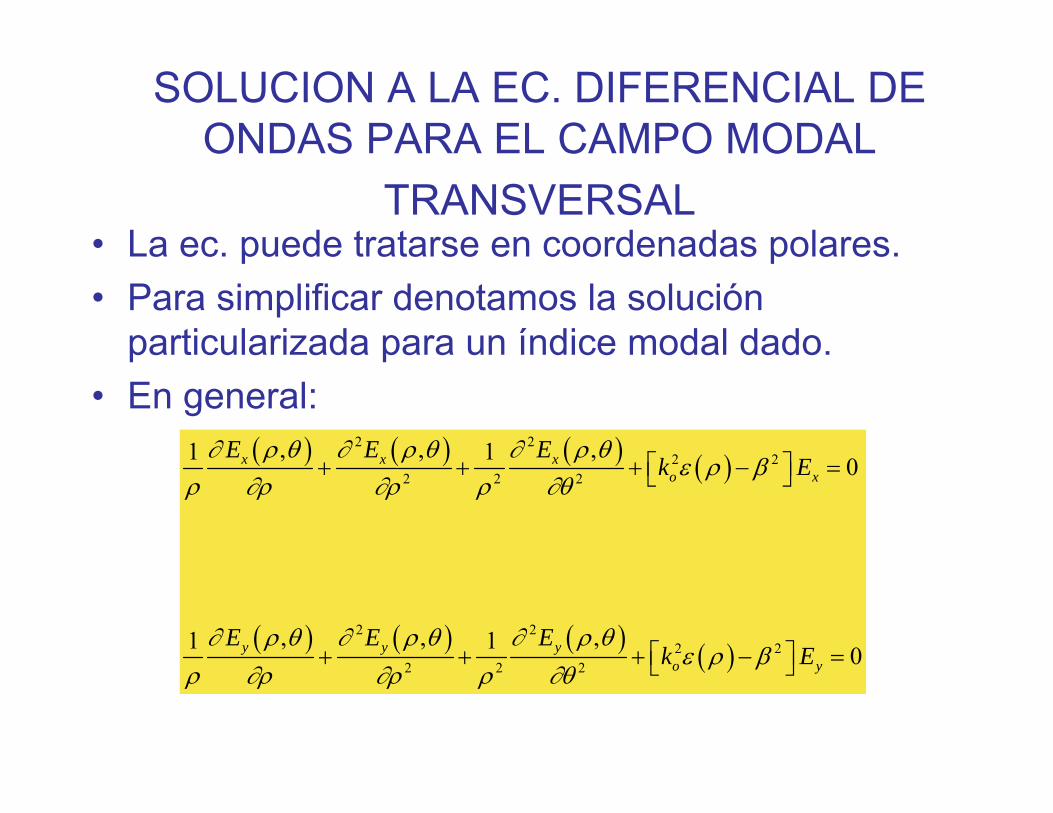
SOLUCION A LA EC. DIFERENCIAL DE ONDAS PARA EL CAMPO MODAL
TRANSVERSAL• La ec. puede tratarse en coordenadas polares.• Para simplificar denotamos la solución
particularizada para un índice modal dado.• En general:
2 22 2
2 2 2
2 22 2
2 2 2
, , ,1 1 0
, , ,1 1 0
x x xo x
y y yo y
E E Ek E
E E Ek E

En particular: Ez es una onda progresiva, se puede
factorizar la dependencia angular:
1 2,zE E E 1 2,zE E E
Se obtiene una solución particular,a partir de la cual se formulan las componentes transversales.
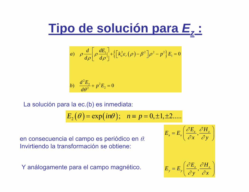
Tipo de solución para Ez :
2 2 2 211
222
22
) 0
) 0
o rdEda k p E
d d
d Eb p Ed
La solución para la ec.(b) es inmediata:
2 exp ; 0, 1, 2.....E in n p
en consecuencia el campo es periódico en Invirtiendo la transformación se obtiene:
,
,
z zx x
z zy y
E HE Ex y
E HE Ey x
Y análogamente para el campo magnético.

SOLUCION PARA LA EC.(a):
La ec.(a) es una ecuación de tipo Bessel:
2
2 2 22 0d dz z z n
dz dz
las soluciones z
son funciones cilíndricas y representan un propagador asociado a geometría cilíndrica.
• De acuerdo con las propiedades de las funciones de Bessel de primera clase y funciones de Hankel de primera y segunda clase:
2 21 n o rE Z k 2 21 n o rE Z k

1.- Funciones de Bessel de primera clase y orden n: nJ
2.- Funciones de Bessel de segunda clase (también llamadas funciones de Weber): nY
3.- Funciones de Bessel de tercera clase (también llamadas funciones de Hankel): , 1
nH 2nH
Estas funciones cumplen determinadas propiedades matemáticas que van a determinar si la solución es del tipo 1), 2) ó 3).En consecuencia, determinan la forma del campo propagándose en la guía.
Propiedades de las funciones de Bessel
1.- Para
•
nJ
; Re 0nJ z n está acotada como 0z para cualquier intervalo finito de
arg z

EJEMPLOS DE FUNCIONES DE BESSEL Y HANKEL
1er cero: 2,405
Tomado de: Abramowitz & Stegun
J0
J1
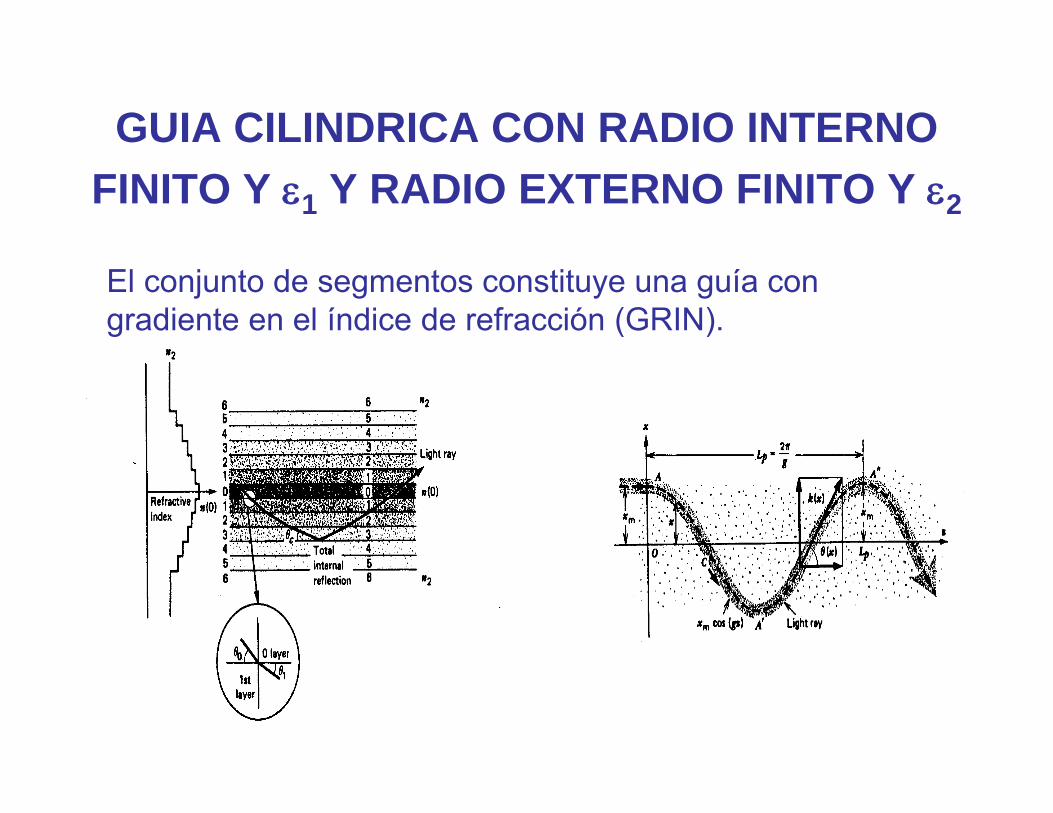
GUIA CILINDRICA CON RADIO INTERNO FINITO Y 1 Y RADIO EXTERNO FINITO Y 2
El conjunto de segmentos constituye una guía con gradiente en el índice de refracción (GRIN).

Guía con gradiente en el índice de refracción: aproximación
nb
nc
O O'Ray1
A
B'
B
A
B
B' Ray2
M
B' c/nb
c/na12
B''
na
a
b
cWe can visualize a graded index
fiber by imagining a stratified
medium with the layers of refractive
indices

Tipo de solución: ecuación de autovalores
22 2
21 1 21 2 1 2
2 2
1k k k Ri i nk k uv
22 2
21 1 21 2 1 2
2 2
1k k k Ri i nk k uv
1
1 2 1
1 1; n n
n n
J Hu uJ v vH
A partir de esta ecuación se obtienen distintos tipos de modos acoplados:MODOS HIBRIDOS.
Frecuencia de corte: u=V; v=0. Raíces de la ec.: Jn = 0 ; J0(2,405) = 0.Guía monomodo: V<2,405.
Caso particular: J1(0)=0. El modo híbrido HE11 no tiene frecuencia de corte.

Diámetro del campo
modal(2W0)
Guía de ondas monomodo,
)/exp()( 20
20 wrErE
Para: r = wo,E(Wo)=Eo/e
Typicamente Wo > a
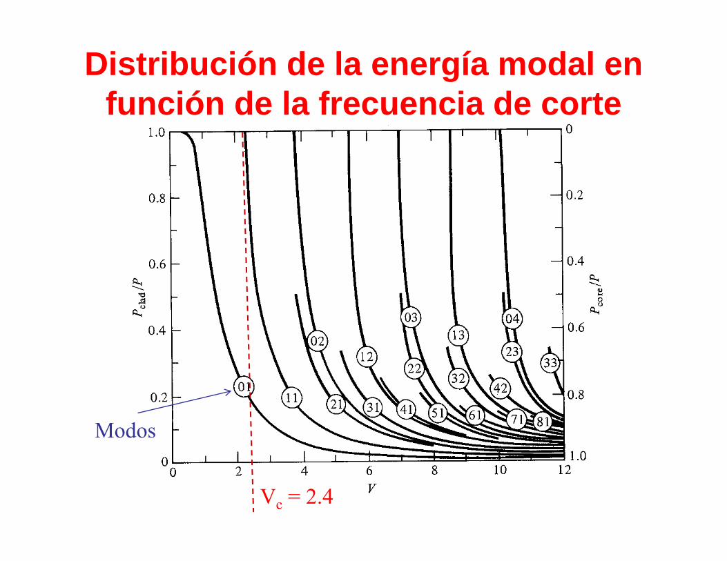
Distribución de la energía modal en función de la frecuencia de corte
Vc = 2.4
Modos

125µm
Different Fiber Types
125µm
10µm
Step Index Fiber Dispersion Shifted Fiber

Dispersión de la señal en guíasde onda ópticas

Wavelength
Wavelength (nm
)
10-4
1
102
104
106
108
1010
10-2
1012
Gamma Rays
X-Rays
Ultraviolet
Visible Light
Infrared
Radiowaves
O-band (1260-1360nm)
E-band (1360-1460nm)
S-band (1460-1530nm)C-band (1530-1560nm)L-band (1560-1625nm)U-band (1625-1675nm)
Ultraviolet Visible
Near infrared
Infrared
Wavelength
(nm)
400
600
800
1000
1200
1400
1600
1800
1st window
2nd window
3rd window

Origen de la dispersión y no-linealidades
• El índice de refracción del material es una función de la frecuencia y de la potencia de la señal luminosa transmitida.
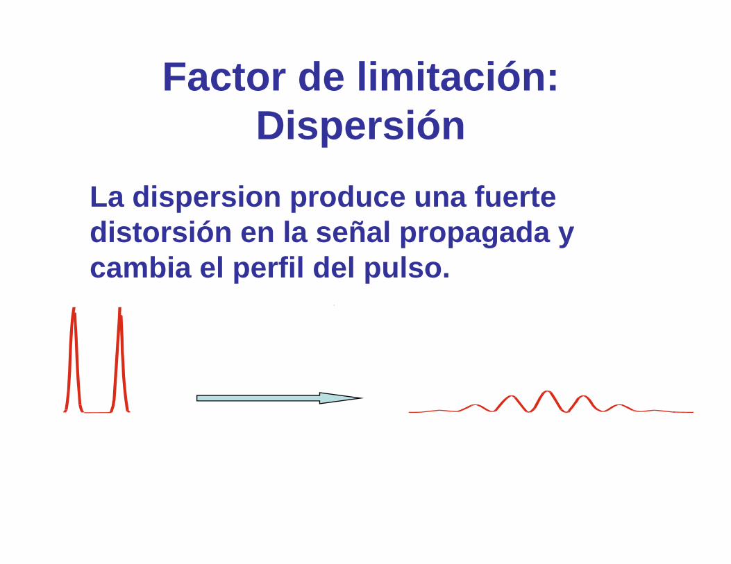
Factor de limitación: Dispersión
La dispersion produce una fuerte distorsión en la señal propagada y cambia el perfil del pulso.
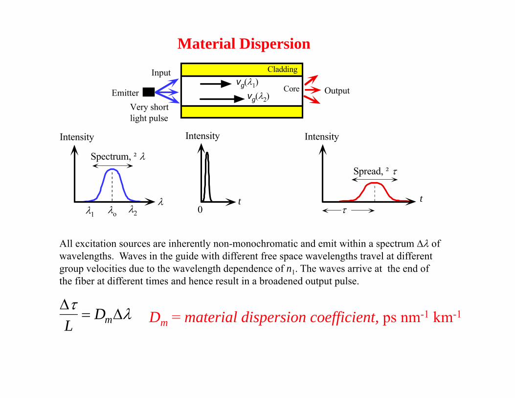
Material Dispersion
All excitation sources are inherently non-monochromatic and emit within a spectrum ∆ of wavelengths. Waves in the guide with different free space wavelengths travel at different group velocities due to the wavelength dependence of n1. The waves arrive at the end of the fiber at different times and hence result in a broadened output pulse.
t
Spread, ²
t0
Spectrum, ²
1 2o
Intensity Intensity Intensity
Cladding
CoreEmitterVery shortlight pulse
vg(2)vg(1)
Input
Output
L
Dm Dm = material dispersion coefficient, ps nm-1 km-1

Waveguide Dispersion
Waveguide dispersion: The group velocity vg(01) of the fundamental mode depends on the V-number which itself depends on the source wavelength even if n1 and n2were constant. Even if n1 and n2 were wavelength independent (no material dispersion), we will still have waveguide dispersion by virtue of vg(01) depending on V and Vdepending inversely on . Waveguide dispersion arises as a result of the guiding properties of the waveguide which imposes a nonlinear -lm relationship.
t
Spread, ²
t0
Spectrum, ²
1 2o
Intensity Intensity Intensity
Cladding
CoreEmitterVery shortlight pulse
vg(2)vg(1)
Input
Output
L
DwDw = waveguide dispersion coefficient
Dw depends on the waveguide structure, ps nm-1 km-1
0
1.2 1.3 1.4 1.5 1.61.1-30
20
30
10
-20
-10
(m)
Dm
Dm + Dw
Dw0
Dispersion coefficient (ps km-1 nm-1)
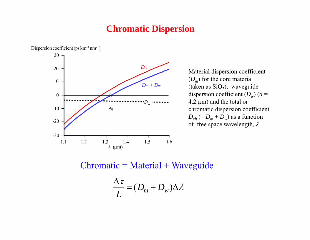
Chromatic Dispersion
Material dispersion coefficient (Dm) for the core material (taken as SiO2), waveguide dispersion coefficient (Dw) (a = 4.2 m) and the total or chromatic dispersion coefficient Dch (= Dm + Dw) as a function of free space wavelength,
L
(Dm Dw)
Chromatic = Material + Waveguide

Material and waveguide dispersion coefficients in anoptical fiber with a core SiO2-13.5%GeO2 for a = 2.5to 4 m.
0
–10
10
20
1.2 1.3 1.4 1.5 1.6–20
(m)
Dm
Dw
SiO2-13.5%GeO2
2.53.03.54.0a (m)
Dispersion coefficient (ps km-1 nm-1)
© 1999 S.O. Kasap, Optoelectronics (Prentice Hall)
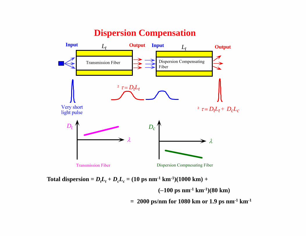
Dispersion Compensation
Very shortlight pulse
Input OutputLt
Transmission Fiber
² DtLt
Lt
Dispersion CompensatingFiber
Input Output
² DtLt + DcLc
Dt
Dc
Transmission Fiber Dispersion Compnesating Fiber
Total dispersion = DtLt + DcLc = (10 ps nm-1 km-1)(1000 km) +
(100 ps nm-1 km-1)(80 km)
= 2000 ps/nm for 1080 km or 1.9 ps nm-1 km-1

k
rL
rL
Geometrical length of the ring
Propagation loss
1
1( )1r zH z
r z
rLe round trip lossrkL round trip phase shift
zzr
pz r
Ejemplo: Ring resonator (RR)
i Directional coupler insertion losski i ir
i ij t
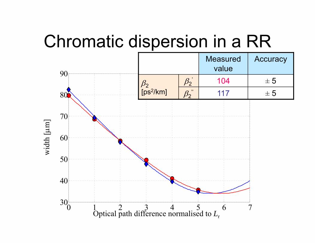
0 1 2 3 4 5 6 730
40
50
60
70
80
90
Measured value
Accuracy
2 [ps2/km]
2’ 104 ± 5
2’’ 117 ± 5
Optical path difference normalised to Lr
wid
th [
m]
Chromatic dispersion in a RR

Core
z
n1x // x
n1y // y
Ey
Ex
Ex
Ey
E
= Pulse spread
Input light pulse
Output light pulset
t
Intensity
Polarization Dispersionn different in different directions due to induced strains in fiber in manufacturing, handling and cabling. n/n 10-6
Dpol L Dpol = polarization dispersion coefficient
Typically Dpol = 0.1 - 0.5 ps nm-1 km-1/2

The refractive index in the middle is larger than at the border
==> the beam with the shortest distance is the slowest one
==> we can optimize the shape of the profile of the refractive index to minimize the multipath time dispersion
Transmission System: Capacity: 6 Gbit/s/km
Reduction of Dispersion (Gradient Index Waveguide)

Fundamentos, diseño e implementación de
dispositivos fotónicosbasados en guías de onda
ópticas

Fourier Transform Arrayed Waveguide Gratings
(FT AWG)• Dispositivo basado en guías de onda planas para
aplicaciones en espectrometría: Spatial Heterodyne Spectrometer (SHS), inicialmente propuesto por P. Chebenet al. en 2003.
• La operación espacial heterodina se realiza con guías de onda de un solo modo (singlemode waveguides).
• Dispositivos basados en interferómetro Mach-Zender (MZI).
• El interferómetro se forma con un array de MZI, cuyadiferencia de camino óptico aumenta progresivamente.

k1 k2
ki i ir
i ij t
Directional coupleri directional coupler
insertion loss
2 2 1i ir t
LL
MZI geometrical unbalance
Propagation loss
Mach Zehnder Interferometer (MZI)

Parámetros para el SHS
Transmisión espectral: T() para cada elemento MZI.
Número de onda:
A y B: coeficientes específicos asociados a la estructura del MZI.
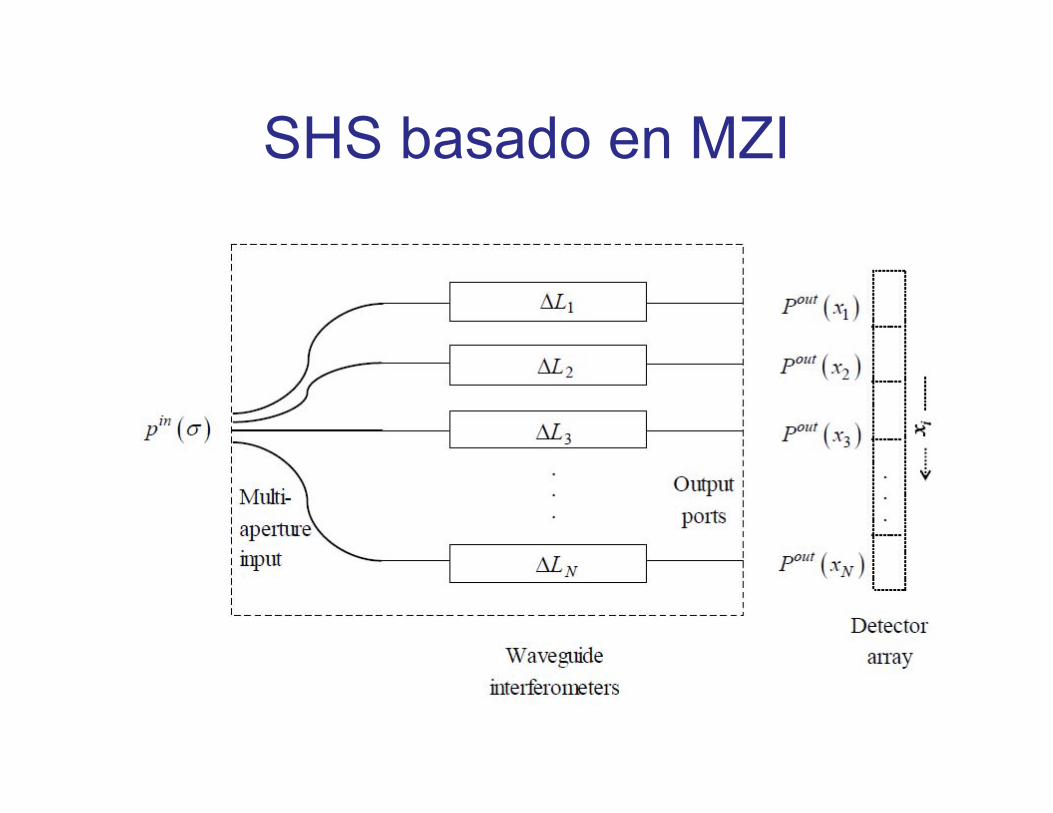
SHS basado en MZI

Señal de salida del MZI• Se forma una
modulación de la señal, dependiendo de la diferencia de camino ópticointroducido en cadaMZI.
• Se observa la formación de franjasde interferencia.

Diseño de la máscara e implementacióndel dispositivo

Dispositivos de guía de onda para análisis espectral: redes, WDM
• Wavelength Division Multiplexing (WDM)[i] is used to increase the amount of data transmitted in an optical fiber by employing multiple wavelengths.
• These different wavelengths, each modulated with a different stream of data, need to be combined (multiplexed) and coupled into the input end of the optical fiber, and then at the output end separated from each other (demultiplexed).
• These two functions are often performed by arrayed waveguide grating optical (de)multiplexers, and more recently also by waveguide echelle grating (de)multiplexers.
• The applications of these devices are not limited to WDM. They can also be used as compact spectrometer chips for applications in spectroscopy, metrology, and chemical and biological sensing, among others.
•[i] Keiser, G. E., Optical Fiber Technology 5, 3-39 (1999).
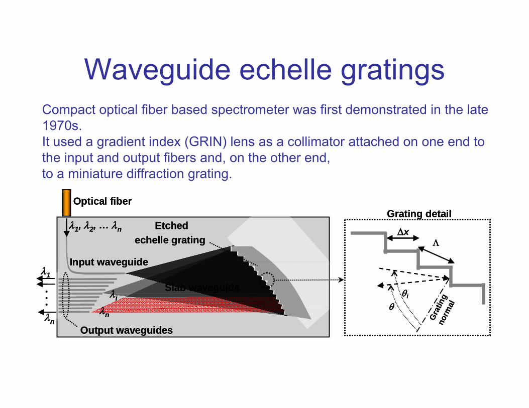
Waveguide echelle gratings
Input waveguide
Output waveguides
1, 2, … n
1
n
...i
n
Slab waveguide
Optical fiber
Etchedechelle grating
x
i
Grating detail
Gra
ting
norm
al
Input waveguide
Output waveguides
1, 2, … n
1
n
...i
n
Slab waveguide
Optical fiber
Etchedechelle grating
x
i
Grating detail
Gra
ting
norm
al
Compact optical fiber based spectrometer was first demonstrated in the late 1970s. It used a gradient index (GRIN) lens as a collimator attached on one end to the input and output fibers and, on the other end, to a miniature diffraction grating.

Aplicaciones a Dispositivos Multiplexadores y Demultiplexadores(*): Diseño optimizado
LN/2
R
j = 0
j = 1
j = N/2
j = N
RLN/2
a
b
L1
LN-1
W0
W1
W0
W1
R(1- Cos(/2))
DispersiveElement
R
R
DT
a) Representation of a divergent-convergent Arrayed Waveguide Grating (AWG) lens-like converser. Focusing points are located at the centre of “circles” defining the input/output apertures. A divergent light beam coming form the focusing point strikes the arrayed waveguides. Phase differences across the entire input aperture remain unchanged. The waveguide number is taking as N+1. Dispersive element will be located at the position showed in the figure.
b) Simplification of the divergent-convergent AWG lens-like converser. Only central N/2 and external Nth-waveguides are represented. Optical path associated to waveguide bend sections, and dispersive element is not taking into account to make a device size reduction to the limit.
(*): P. Cheben et al. OPTOEL’05, Elche, Julio 2005

• The input and output channel waveguides join the slab waveguide at the Rowland circle.
• The light from the input waveguide is coupled into the slab waveguide where it diverges in the waveguide plane, illuminating the grating.
•The light is diffracted backward from the concave (focusing) grating.
Since the grating is used in the reflection geometry, the grating facets are metallized to increase efficiency.
Modifications of the Waveguide geometry

Grating geometry

Grating equation• In a grating spectrometer, the light propagates as an
optical mode guided in the slab waveguide of effective index neff.
• The grating is etched through the waveguide layers in the direction z perpendicular to the waveguide plane xy.
• The grating facets are often metal-coated to improve reflectivity so that each facet acts as a small mirror reflecting the incident light according the laws of reflection.
• The light reflected by different facets will add in phase hence producing interference maxima in those directions for which the phase difference between the light diffracted by two adjacent facets is 2m.
• This is expressed by the scalar grating equation

Scalar grating equation
• where i is the angle of incidence, is the wavelength measured in vacuum, is the grating period (pitch), and m = 0, ±1, ±2, … is the diffraction order.
• For gratings with small ratios /, many diffraction orders may exist.
• Such gratings are called echelle gratings and their important characteristics are large dispersion and resolution.
effi n
m sinsin

Grating Angular Dispersion• By differentiating the grating equation:
)cos/(/ effnmdd
The grating resolution, R = /, also called resolving power,is the ability of a grating to separate adjacent wavelengths.
• The definition of grating resolving power is obtained using Rayleigh criterion: the two peaks of wavelengths and + are considered resolved if their far fields are angularly separated by at least the half-width of the far-field diffraction pattern.
~ /(Lneff cos).
• In (de)multiplexers, the adjacent channels need to be separated more than this Rayleigh limit in order to minimize the inter-channel crosstalk.

Concave Grating in a Rowland Circle Configuration
• The grating linear dispersion is:
• r: radius of the Rowland circle• Resolution and dispersion increase with diffraction order
m at which the grating operates.• For WDM applications, m ~ 20 is typically sufficient for
(de)multiplexing of wavelength channels separated at 100 GHz.
)1(sin4
d
dnn
rddyD eff
eff

Channel Passband
• Is the spectral dependence of the coupling efficiency for a given wavelength.
• Is determined by the convolution of the focal field and the output waveguide mode distributions.
• The focal field is coupled to the fundamental mode of the output waveguide with a coupling efficiency given by the overlap integral of the focal field and the output waveguide mode spatial distributions.
• For a concave (focusing) grating, the light spatial distribution in the focal region is approximately Gaussian at a given wavelength.
• Since both distributions are nearly Gaussian, the channel passband is also, to a good approximation, Gaussian.

Typical Gaussian Channel Passband
Channel spacing
Channel phase error

Arrayed waveguide gratings• Is an optical analogue of a microwave phased array antenna: by controlling the
phase relationship between radiating sources forming the array output, the radiated beam direction can be changed without mechanical movement.
• The AWG was invented in 1988 by Meint . K. Smit • (Eindhoven, Holland).
• Along with the semiconductor lasers, the AWG is one of the most complex, superbly developed, and commercially successful planar waveguide devices.
• The AWG is a key device in WDM optical communication systems.
• It performs functions such as wavelength multiplexing and demultiplexing, wavelength filtering, signal routing, and optical cross-connects.
• AWGs are also increasingly used in areas other than WDM, such as signal processing, spectral analysis, and sensing.

Schematic of an AWG operating as a WD
Waveguide array
Modified region(optional)
Input combiner Output
combiner
Input waveguide n
Output waveguidesn
Input phasefront
Output phasefront,radius f
Rowland circle,radius r = f/2
fA
C - B = |BC|2neff,slab /
B - A = 2m (phasefront)
Output combiner(slab waveguide)
Waveguide aray
Phasefront
a
B
C
b
C - A = 2Lneff,array /
x
Array-slab boundary,radius f = 2r
Detail of the phased array out put aperture

AWG Equivalent Grating Equation
• Where is the waveguide pitch at the output of the phased array and neff,s is the slab waveguide effective index. L is the length difference (constant) between the adjacent waveguides.neff,a is the effective index of an arrayed waveguide.
mLnn aeffseff ,, sin

Examples of planar optical waveguides
a) glass buried channel waveguide (silica-on-silicon), b) silicon-on-insulator (SOI) ridge waveguide, and c) deep ridge waveguide in InGaAsP/InP.

Modified devices and applications
a) An optical microphotograph of a high-resolution SOI AWG microspectrometer b) and c) Narrow rectangular waveguides at the input and focal regions.
d) Measured microspectrometer spectra [Source: P. Cheben et al., Opt. Express, vol. 15, p. 2299, 2007].

References
• P. Cheben, “Walength dispersive planar waveguides devices: Echelle and arrayed waveguide gratings”, in: Optical Waveguides from Theory to Applied Technologies, (Calvo, Lakshminarayanan, Eds.), CRC Press, New York, 2007, Chapter 5.