슬라이드 제목 없음 - lcd-source.comDisplay/LM240WU7-SLB3.pdfIt has been designed to apply...
34
Product Specification LM240WU7 Liquid Crystal Display Ver. 0.1 Feb. 28 . 2011 1 / 34 SPECIFICATION FOR APPROVAL (●) Preliminary Specification ( ) Final Specification 24.0” WUXGA TFT LCD Title MODEL BUYER SUPPLIER LG Display Co., Ltd. *MODEL LM240WU7 SUFFIX SLB3 *When you obtain standard approval, please use the above model name without suffix HP APPROVED BY SIGNATURE DATE / / / Please return 1 copy for your confirmation with your signature and comments. B.C KIM / G.Manager MNT Products Engineering Dept. LG Display Co., Ltd. APPROVED BY SIGNATURE DATE REVIEWED BY PREPARED BY S.H KIM / Manager [C] T.K KIM / Engineer I.M. Choi / Manager [P] Y.H HWANG / Manager [M] www.jxlcd.com www.jxlcd.com
Transcript of 슬라이드 제목 없음 - lcd-source.comDisplay/LM240WU7-SLB3.pdfIt has been designed to apply...
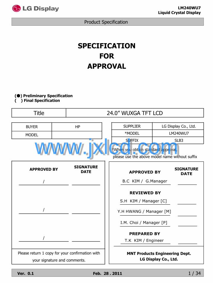
Product Specification
LM240WU7Liquid Crystal Display
Ver. 0.1 Feb. 28 . 2011 1 / 34
SPECIFICATION
FOR
APPROVAL
(●) Preliminary Specification( ) Final Specification
24.0” WUXGA TFT LCDTitle
MODEL
BUYER SUPPLIER LG Display Co., Ltd.
*MODEL LM240WU7
SUFFIX SLB3
*When you obtain standard approval,
please use the above model name without suffix
HP
APPROVED BYSIGNATURE
DATE
/
/
/
Please return 1 copy for your confirmation with
your signature and comments.
B.C KIM / G.Manager
MNT Products Engineering Dept.
LG Display Co., Ltd.
APPROVED BYSIGNATURE
DATE
REVIEWED BY
PREPARED BY
S.H KIM / Manager [C]
T.K KIM / Engineer
I.M. Choi / Manager [P]
Y.H HWANG / Manager [M]
www.jxlcd.comwww.jxlcd.com
Product Specification
LM240WU7Liquid Crystal Display
Ver. 0.1 Feb. 28 . 2011 2 / 34
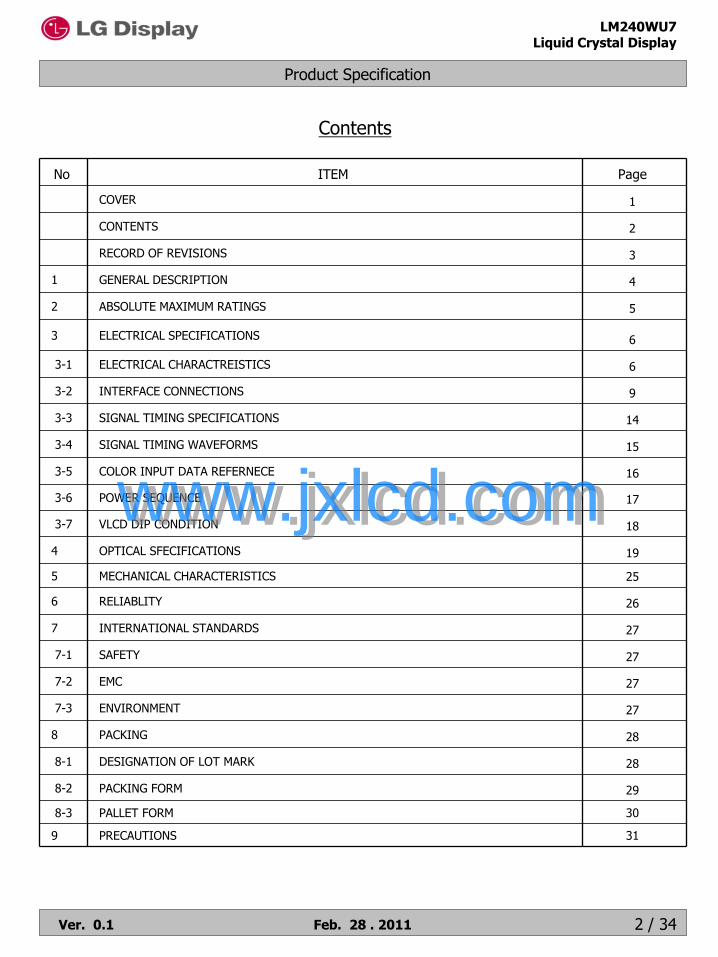
Contents
No ITEM Page
COVER 1
CONTENTS 2
RECORD OF REVISIONS 3
1 GENERAL DESCRIPTION 4
2 ABSOLUTE MAXIMUM RATINGS 5
3 ELECTRICAL SPECIFICATIONS 6
3-1 ELECTRICAL CHARACTREISTICS 6
3-2 INTERFACE CONNECTIONS 9
3-3 SIGNAL TIMING SPECIFICATIONS 14
3-4 SIGNAL TIMING WAVEFORMS 15
3-5 COLOR INPUT DATA REFERNECE 16
3-6 POWER SEQUENCE 17
3-7 VLCD DIP CONDITION 18
4 OPTICAL SFECIFICATIONS 19
5 MECHANICAL CHARACTERISTICS 25
6 RELIABLITY 26
7 INTERNATIONAL STANDARDS 27
7-1 SAFETY 27
7-2 EMC 27
7-3 ENVIRONMENT 27
8 PACKING 28
8-1 DESIGNATION OF LOT MARK 28
8-2 PACKING FORM 29
8-3 PALLET FORM 30
9 PRECAUTIONS 31
www.jxlcd.comwww.jxlcd.com

Product Specification
LM240WU7Liquid Crystal Display
Ver. 0.1 Feb. 28 . 2011 3 / 34
RECORD OF REVISIONS
Revision No
Revision Date Page Description
0.0 Dec. 08.2010 - First Draft (Preliminary)
0.1 Feb. 28. 2011 19 Update color coordinates
27 Update Mechanical drawings
30 Update Designation of Lot Mark
www.jxlcd.comwww.jxlcd.com
Product Specification
LM240WU7Liquid Crystal Display
Ver. 0.1 Feb. 28 . 2011 4 / 34
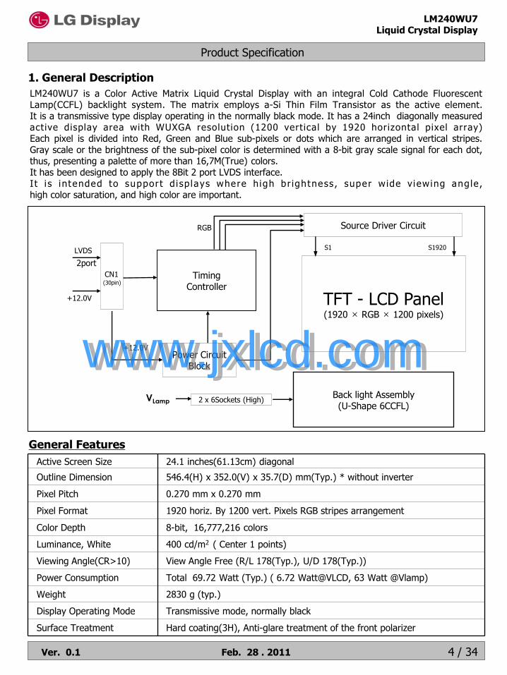
1. General Description
General Features
Active Screen Size 24.1 inches(61.13cm) diagonal
Outline Dimension 546.4(H) x 352.0(V) x 35.7(D) mm(Typ.) * without inverter
Pixel Pitch 0.270 mm x 0.270 mm
Pixel Format 1920 horiz. By 1200 vert. Pixels RGB stripes arrangement
Color Depth 8-bit, 16,777,216 colors
Luminance, White 400 cd/m2 ( Center 1 points)
Viewing Angle(CR>10) View Angle Free (R/L 178(Typ.), U/D 178(Typ.))
Power Consumption Total 69.72 Watt (Typ.) ( 6.72 Watt@VLCD, 63 Watt @Vlamp)
Weight 2830 g (typ.)
Display Operating Mode Transmissive mode, normally black
Surface Treatment Hard coating(3H), Anti-glare treatment of the front polarizer
LM240WU7 is a Color Active Matrix Liquid Crystal Display with an integral Cold Cathode FluorescentLamp(CCFL) backlight system. The matrix employs a-Si Thin Film Transistor as the active element.It is a transmissive type display operating in the normally black mode. It has a 24inch diagonally measuredactive display area with WUXGA resolution (1200 vertical by 1920 horizontal pixel array)Each pixel is divided into Red, Green and Blue sub-pixels or dots which are arranged in vertical stripes.Gray scale or the brightness of the sub-pixel color is determined with a 8-bit gray scale signal for each dot,thus, presenting a palette of more than 16,7M(True) colors. It has been designed to apply the 8Bit 2 port LVDS interface.I t i s intended to suppor t d isp lays where high br ightness , super wide viewing angle,high color saturation, and high color are important.
CN1(30pin)
LVDS
2port
+12.0V
Power Circuit Block
Source Driver Circuit
TFT - LCD Panel(1920 × RGB × 1200 pixels)
S1 S1920
RGB
TimingController
+12.0V
Back light Assembly(U-Shape 6CCFL)
2 x 6Sockets (High)VLamp
www.jxlcd.comwww.jxlcd.com
Product Specification
LM240WU7Liquid Crystal Display
Ver. 0.1 Feb. 28 . 2011 5 / 34
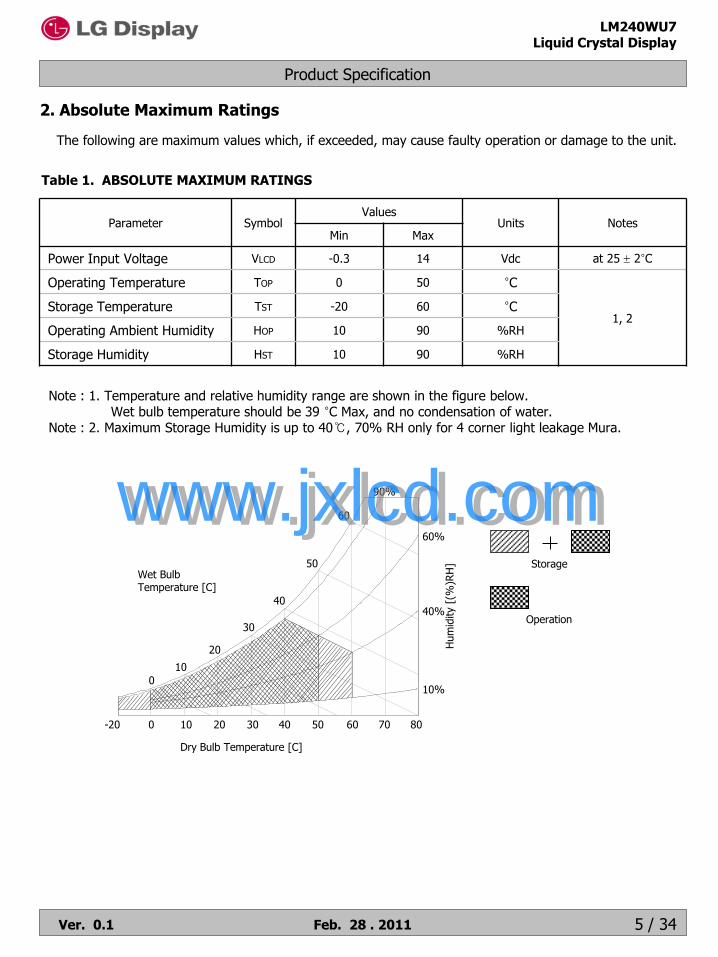
2. Absolute Maximum Ratings
The following are maximum values which, if exceeded, may cause faulty operation or damage to the unit.
Note : 1. Temperature and relative humidity range are shown in the figure below. Wet bulb temperature should be 39 °C Max, and no condensation of water.
Note : 2. Maximum Storage Humidity is up to 40℃, 70% RH only for 4 corner light leakage Mura.
Table 1. ABSOLUTE MAXIMUM RATINGS
Parameter SymbolValues
Units NotesMin Max
Power Input Voltage VLCD -0.3 14 Vdc at 25 2°C
Operating Temperature TOP 0 50 °C
1, 2Storage Temperature TST -20 60 °C
Operating Ambient Humidity HOP 10 90 %RH
Storage Humidity HST 10 90 %RH
90%
10 20 30 40 50 60 70 800-20
0
10
20
30
40
50
Dry Bulb Temperature [C]
Wet BulbTemperature [C]
Storage
Operation
Hum
idity [
(%)R
H]
10%
40%
60%
60www.jxlcd.comwww.jxlcd.com
Product Specification
LM240WU7Liquid Crystal Display
Ver. 0.1 Feb. 28 . 2011 6 / 34
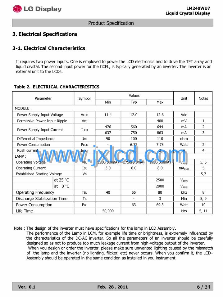
3. Electrical Specifications
3-1. Electrical Characteristics
Table 2. ELECTRICAL CHARACTERISTICS
It requires two power inputs. One is employed to power the LCD electronics and to drive the TFT array and liquid crystal. The second input power for the CCFL, is typically generated by an inverter. The inverter is an external unit to the LCDs.
Parameter SymbolValues
Unit NotesMin Typ Max
MODULE :
Power Supply Input Voltage VLCD 11.4 12.0 12.6 Vdc
Permissive Power Input Ripple VRF 400 mV 1
Power Supply Input Current ILCD476 560 644 mA 2
637 750 863 mA 3
Differential Impedance Zm 90 100 110 ohm
Power Consumption PLCD - 6.72 7.73 Watt 2
Rush current IRUSH - - 3 A 4
LAMP :
Operating Voltage VBL 1550(8.0mA) 1750(6.0mA) 1950(3.0mA) VRMS 5, 6
Operating Current IBL 3.0 6.0 8.0 mARMS 5
Established Starting Voltage Vs 5,7
at 25 °C 2500 VRMS
at 0 °C 2900 VRMS
Operating Frequency fBL 40 55 80 kHz 8
Discharge Stabilization Time Ts - 3 Min 5, 9
Power Consumption PBL 63 69.3 Watt 10
Life Time 50,000 Hrs 5, 11
Note : The design of the inverter must have specifications for the lamp in LCD Assembly.The performance of the Lamp in LCM, for example life time or brightness, is extremely influenced bythe characteristics of the DC-AC inverter. So all the parameters of an inverter should be carefullydesigned so as not to produce too much leakage current from high-voltage output of the inverter.When you design or order the inverter, please make sure unwanted lighting caused by the mismatch
of the lamp and the inverter (no lighting, flicker, etc) never occurs. When you confirm it, the LCD–Assembly should be operated in the same condition as installed in you instrument.
www.jxlcd.comwww.jxlcd.com
Product Specification
LM240WU7Liquid Crystal Display
Ver. 0.1 Feb. 28 . 2011 7 / 34
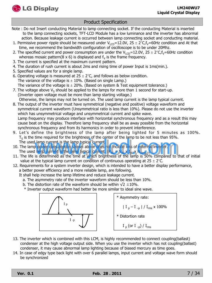
Note : Do not Insert conducting Material to lamp connecting socket. If the conducting Material is inserted to the lamp connecting sockets, TFT-LCD Module has a low luminance and the inverter has abnormal
action. Because leakage current is occurred between lamp connecting socket and conducting material.1. Permissive power ripple should be measured under VLCD=12.0V, 25 2°C,fV=60Hz condition and At that
time, we recommend the bandwidth configuration of oscilloscope is to be under 20Mhz.2. The specified current and power consumption are under the VLCD=12.0V, 25 2°C,fV=60Hz condition
whereas mosaic pattern(8 x 6) is displayed and fV is the frame frequency.3. The current is specified at the maximum current pattern.4. The duration of rush current is about 2ms and rising time of power Input is 1ms(min.).5. Specified values are for a single lamp.6. Operating voltage is measured at 25 2°C, and follows as below condition.
The variance of the voltage is 10%. (Based on single Lamp.)The variance of the voltage is 20%. (Based on system & Test equipment tolerance.)
7. The voltage above VS should be applied to the lamps for more than 1 second for start-up.(Inverter open voltage must be more than lamp starting voltage.)Otherwise, the lamps may not be turned on. The used lamp current is the lamp typical current.
8. The output of the inverter must have symmetrical (negative and positive) voltage waveform andsymmetrical current waveform (Unsymmetrical ratio is less than 10%). Please do not use the inverter which has unsymmetrical voltage and unsymmetrical current and spike wave. Lamp frequency may produce interface with horizontal synchronous frequency and as a result this maycause beat on the display. Therefore lamp frequency shall be as away possible from the horizontalsynchronous frequency and from its harmonics in order to prevent interference.
9. Let‟s define the brightness of the lamp after being l ighted for 5 minutes as 100%.TS is the time required for the brightness of the center of the lamp to be not less than 95%.The used lamp current is the lamp typical current.
10. The lamp power consumption shown above does not include loss of external inverter.The used lamp current is the lamp typical current. (PBL = VBL x IBL x NLamp )
11. The life is determined as the time at which brightness of the lamp is 50% compared to that of initialvalue at the typical lamp current on condition of continuous operating at 25 2°C.
12. Requirements for a system inverter design, which is intended to have a better display performance, a better power efficiency and a more reliable lamp, are following. It shall help increase the lamp lifetime and reduce leakage current.
a. The asymmetry rate of the inverter waveform should be less than 10%. b. The distortion rate of the waveform should be within √2 ±10%. * Inverter output waveform had better be more similar to ideal sine wave.
I p
I -p
* Asymmetry rate:
| I p – I –p | / Irms x 100%
* Distortion rate
I p (or I –p) / Irms
13. The inverter which is combined with this LCM, is highly recommended to connect coupling(ballast) condenser at the high voltage output side. When you use the inverter which has not coupling(ballast) condenser, it may cause abnormal lamp lighting because of biased mercury as time goes.
14. In case of edgy type back light with over 6 parallel lamps, input current and voltage wave form should be synchronized
www.jxlcd.comwww.jxlcd.com

Product Specification
LM240WU7Liquid Crystal Display
Ver. 0.1 Feb. 28 . 2011 8 / 34
Mosaic Pattern(8 x 6)
Typical current pattern
(White : 255Gray, Black : 0Gray)Maximum current pattern
White Pattern
< Power consumption (VLCD=12.0V, 25 2°C,fV=60Hz) >
Black Pattern
< Permissive Power Input Ripple (VLCD=12.0V, 25 2°C,fV=60Hz) >
White Pattern
[ Figure 3 ] Mosaic pattern & Black Pattern for power consumption measurement
www.jxlcd.comwww.jxlcd.com

Product Specification
LM240WU7Liquid Crystal Display
Ver. 0.1 Feb. 28 . 2011 9 / 34
3-2. Interface Connections
Table 3 MODULE CONNECTOR(CN1) PIN CONFIGURATION
- LCD Connector(CN1) : IS100-L30B-C23 (UJU), KDF71G-30S-1H (Hirose ) or Equivalent
- Mating Connector : FI-X30C2L (Manufactured by JAE) or Equivalent
3-2-1. LCD Module
Note: 1. All GND(ground) pins should be connected together and to Vss which should also be connected to the LCD‟s metal frame.
2. All VLCD (power input) pins should be connected together.3. Input Level of LVDS signal is based on the EIA 664 Standard.
No Symbol Description No Symbol Description
1 FR0M Minus signal of odd channel 0 (LVDS) 16 SR1P Plus signal of even channel 1 (LVDS)
2 FR0P Plus signal of odd channel 0 (LVDS) 17 GND Ground
3 FR1M Minus signal of odd channel 1 (LVDS) 18 SR2M Minus signal of even channel 2 (LVDS)
4 FR1P Plus signal of odd channel 1 (LVDS) 19 SR2P Plus signal of even channel 2 (LVDS)
5 FR2M Minus signal of odd channel 2 (LVDS) 20 SCLKINM Minus signal of even clock channel (LVDS)
6 FR2P Plus signal of odd channel 2 (LVDS) 21 SCLKINP Plus signal of even clock channel (LVDS)
7 GND Ground 22 SR3M Minus signal of even channel 3 (LVDS)
8 FCLKINM Minus signal of odd clock channel (LVDS) 23 SR3P Plus signal of even channel 3 (LVDS)
9 FCLKINP Plus signal of odd clock channel (LVDS) 24 GND Ground
10 FR3M Minus signal of odd channel 3 (LVDS) 25 OPEN NC
11 FR3P Plus signal of odd channel 3 (LVDS) 26 OPEN NC
12 SR0M Minus signal of even channel 0 (LVDS) 27 PWM PWM_OUT for Wavy Noise
13 SR0P Plus signal of even channel 0 (LVDS) 28 ODC ONODC ON/OFF ControlH : ODC ON , L : ODC OFF(Connect High or Low.No NC Condition)
14 GND Ground 29 VLCD Power Supply +12.0V
15 SR1M Minus signal of even channel 1 (LVDS) 30 VLCD Power Supply +12.0V
301
User Connector Diagram
IS100-L30B-C23(UJU)
#1 #30
Rear view of LCM
www.jxlcd.comwww.jxlcd.com
Product Specification
LM240WU7Liquid Crystal Display
Ver. 0.1 Feb. 28 . 2011 10 / 34
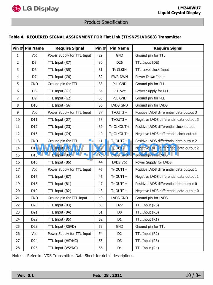
Table 4. REQUIRED SIGNAL ASSIGNMENT FOR Flat Link (TI:SN75LVDS83) Transmitter
Notes : Refer to LVDS Transmitter Data Sheet for detail descriptions.
Pin # Require SignalPin Name Pin # Require SignalPin Name
1 Power Supply for TTL InputVCC 29 Ground pin for TTLGND
2 TTL Input (R7)D5 30 TTL Input (DE)D26
3 TTL Input (R5)D6 31 TTL Level clock InputTX CLKIN
4 TTL Input (G0)D7 32 Power Down InputPWR DWN
5 Ground pin for TTLGND 33 Ground pin for PLLPLL GND
6 TTL Input (G1)D8 34 Power Supply for PLLPLL VCC
7 TTL Input (G2)D9 35 Ground pin for PLLPLL GND
8 TTL Input (G6)D10 36 Ground pin for LVDSLVDS GND
9 Power Supply for TTL InputVCC 37 Positive LVDS differential data output 3TxOUT3+
10 TTL Input (G7)D11 38 Negative LVDS differential data output 3TxOUT3-
11 TTL Input (G3)D12 39 Positive LVDS differential clock outputTX CLKOUT+
12 TTL Input (G4)D13 40 Negative LVDS differential clock outputTX CLKOUT-
13 Ground pin for TTLGND 41 Positive LVDS differential data output 2TX OUT2+
14 TTL Input (G5)D14 42 Negative LVDS differential data output 2TX OUT2-
15 TTL Input (B0)D15 43 Ground pin for LVDSLVDS GND
16 TTL Input (B6)D16 44 Power Supply for LVDSLVDS VCC
17 Power Supply for TTL InputVCC 45 Positive LVDS differential data output 1TX OUT1+
46 Negative LVDS differential data output 1TX OUT1-18 TTL Input (B7)D17
47 Positive LVDS differential data output 0TX OUT0+
48 Negative LVDS differential data output 0TX OUT0-
19 TTL Input (B1)D18
20 TTL Input (B2)D19
49 Ground pin for LVDSLVDS GND21 Ground pin for TTL InputGND
22 TTL Input (B3)D20
23 TTL Input (B4)D21
50 TTL Input (R6)D27
51 TTL Input (R0)D0
24 TTL Input (B5)D22
25 TTL Input (RSVD)D23
52 TTL Input (R1)D1
53 Ground pin for TTLGND
26 Power Supply for TTL InputVCC 54 TTL Input (R2)D2
55 TTL Input (R3)D327 TTL Input (HSYNC)D24
56 TTL Input (R4)D428 TTL Input (VSYNC)D25
www.jxlcd.comwww.jxlcd.com
Product Specification
LM240WU7Liquid Crystal Display
Ver. 0.1 Feb. 28 . 2011 11 / 34
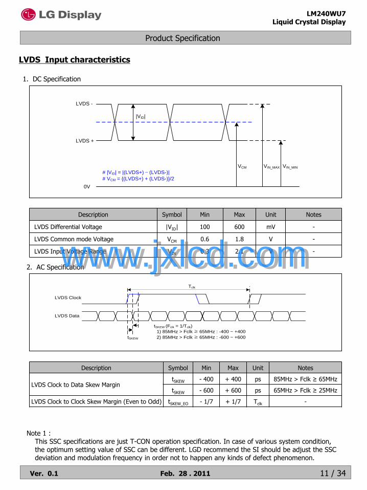
LVDS Input characteristics
Description Symbol Min Max Unit Notes
LVDS Clock to Data Skew MargintSKEW - 400 + 400 ps 85MHz > Fclk ≥ 65MHz
tSKEW - 600 + 600 ps 65MHz > Fclk ≥ 25MHz
LVDS Clock to Clock Skew Margin (Even to Odd) tSKEW_EO - 1/7 + 1/7 Tclk -
Description Symbol Min Max Unit Notes
LVDS Differential Voltage |VID| 100 600 mV -
LVDS Common mode Voltage VCM 0.6 1.8 V -
LVDS Input Voltage Range VIN 0.3 2.1 V -
1. DC Specification
LVDS Data
tSKEW
LVDS Clock
Tclk
tSKEW (Fclk = 1/Tclk)
1) 85MHz > Fclk ≥ 65MHz : -400 ~ +400
2) 85MHz > Fclk ≥ 65MHz : -600 ~ +600
2. AC Specification
LVDS +
LVDS -
0V
VCM
# |VID| = |(LVDS+) – (LVDS-)|
# VCM = {(LVDS+) + (LVDS-)}/2
|VID|
VIN_MAX VIN_MIN
Note 1 : This SSC specifications are just T-CON operation specification. In case of various system condition, the optimum setting value of SSC can be different. LGD recommend the SI should be adjust the SSC deviation and modulation frequency in order not to happen any kinds of defect phenomenon.
www.jxlcd.comwww.jxlcd.com
Product Specification
LM240WU7Liquid Crystal Display
Ver. 0.1 Feb. 28 . 2011 12 / 34
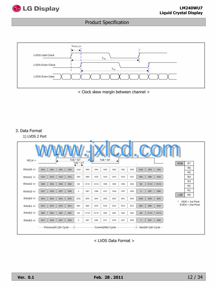
LVDS Even Data
LVDS Odd Clock
LVDS Even Clock
tSKEW_EO
Tclk
Tclk
< Clock skew margin between channel >
OG0 OR5 OR4 OR3 OR2 OR1 OR0
OB1 OB0 OG5 OG4 OG3 OG2 OG1
DE VSYNC HSYNC OB5 OB4 OB3 OB2
X OB7 OB6 OG7 OG6 OR7 OR6
Current(Nth) CyclePrevious(N-1)th Cycle Next(N+1)th Cycle
RCLK +
RXinO0 +/-
Tclk * 4/7 Tclk * 3/7
Tclk
Tclk * 1/7 MSB R7
R6
R5
R4
R3
R2
R1
R0LSB
EG0 ER5 ER4 ER3 ER2 ER1 ER0
EB1 EB0 EG5 EG4 EG3 EG2 EG1
DE VSYNC HSYNC EB5 EB4 EB3 EB2
X EB7 EB6 EG7 EG6 ER7 ER6
* ODD = 1st Pixel
EVEN = 2nd Pixel
RXinO1 +/-
RXinO2 +/-
RXinO3 +/-
RXinE0 +/-
RXinE1 +/-
RXinE2 +/-
RXinE3 +/-
OR3 OR2 OR1 OR0
OG4 OG3 OG2 OG1
OB5 OB4 OB3 OB2
OG7 OG6 OR7 OR6
ER3 ER2 ER1 ER0
EG4 EG3 EG2 EG1
EB5 EB4 EB3 EB2
EG7 EG6 ER7 ER6
OG0 OR5 OR4
OB1 OB0 OG5
DE VSYNC HSYNC
X OB7 OB6
EG0 ER5 ER4
EB1 EB0 EG5
DE VSYNC HSYNC
X EB7 EB6
< LVDS Data Format >
3. Data Format
1) LVDS 2 Port
www.jxlcd.comwww.jxlcd.com

Product Specification
LM240WU7Liquid Crystal Display
Ver. 0.1 Feb. 28 . 2011 13 / 34
2) LVDS 1 Port
G0 R5 R4 R3 R2 R1 R0
B1 B0 G5 G4 G3 G2 G1
DE VSYNC HSYNC B5 B4 B3 B2
X B7 B6 G7 G6 R7 R6
R1 R0
G2 G1
B3 B2
R7 R6
G0
B1
DE
X
Current (Nth ) Cycle
R5 R4
B0 G5
VSYNC HSYNC
B7 B6
R3 R2
G4 G3
B5 B4
G7 G6
Previous (N-1)th Cycle Next (N+1)th Cycle
RCLK+
RA+/-
RB+/-
RC+/-
RD+/-
www.jxlcd.comwww.jxlcd.com
Product Specification
LM240WU7Liquid Crystal Display
Ver. 0.1 Feb. 28 . 2011 14 / 34
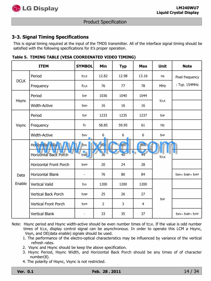
3-3. Signal Timing Specifications
This is signal timing required at the input of the TMDS transmitter. All of the interface signal timing should besatisfied with the following specifications for it‟s proper operation.
Table 5. TIMING TABLE (VESA COORDINATED VIDEO TIMING)
ITEM SYMBOL Min Typ Max Unit Note
DCLK
Period tCLK 12.82 12.98 13.16 ns Pixel frequency
: Typ. 154MHz Frequency fCLK 76 77 78 MHz
Hsync
Period tHP 1036 1040 1044
tCLK
Width-Active tWH 16 16 16
Vsync
Period tVP 1233 1235 1237 tHP
Frequency fV 58.85 59.95 61 Hz
Width-Active tWV 6 6 6 tHP
Data
Enable
Horizontal Valid tHV 960 960 960
tCLKHorizontal Back Porch tHBP 36 40 44
Horizontal Front Porch tHFP 20 24 28
Horizontal Blank - 76 80 84 tWH+ tHBP+ tHFP
Vertical Valid tVV 1200 1200 1200
tHP
Vertical Back Porch tVBP 25 26 27
Vertical Front Porch tVFP 2 3 4
Vertical Blank - 33 35 37 tWV+ tVBP+ tVFP
Note: Hsync period and Hsync width-active should be even number times of tCLK. If the value is odd numbertimes of tCLK, display control signal can be asynchronous. In order to operate this LCM a Hsync,Vsyn, and DE(data enable) signals should be used.
1. The performance of the electro-optical characteristics may be influenced by variance of the verticalrefresh rates.
2. Vsync and Hsync should be keep the above specification.3. Hsync Period, Hsync Width, and Horizontal Back Porch should be any times of of character
number(8).4. The polarity of Hsync, Vsync is not restricted.
www.jxlcd.comwww.jxlcd.com
Product Specification
LM240WU7Liquid Crystal Display
Ver. 0.1 Feb. 28 . 2011 15 / 34
3-4. Signal Timing Waveforms
Dclk
Hsync, Vsync, DE, DATA
tCLK0.5VDD
VALID
INVALIDINVALID
DE(Data Enable)
0.7VDD
0.3VDD
DATA
Data are latched at the falling edge of DCLK
Hsync
DE(Data Enable)
DE(Data Enable)
tWH
tHP
tHFPtHBP
tVP
tWV
tVBPtVFP
tHV
tVV
Vsync
www.jxlcd.comwww.jxlcd.com
Product Specification
LM240WU7Liquid Crystal Display
Ver. 0.1 Feb. 28 . 2011 16 / 34
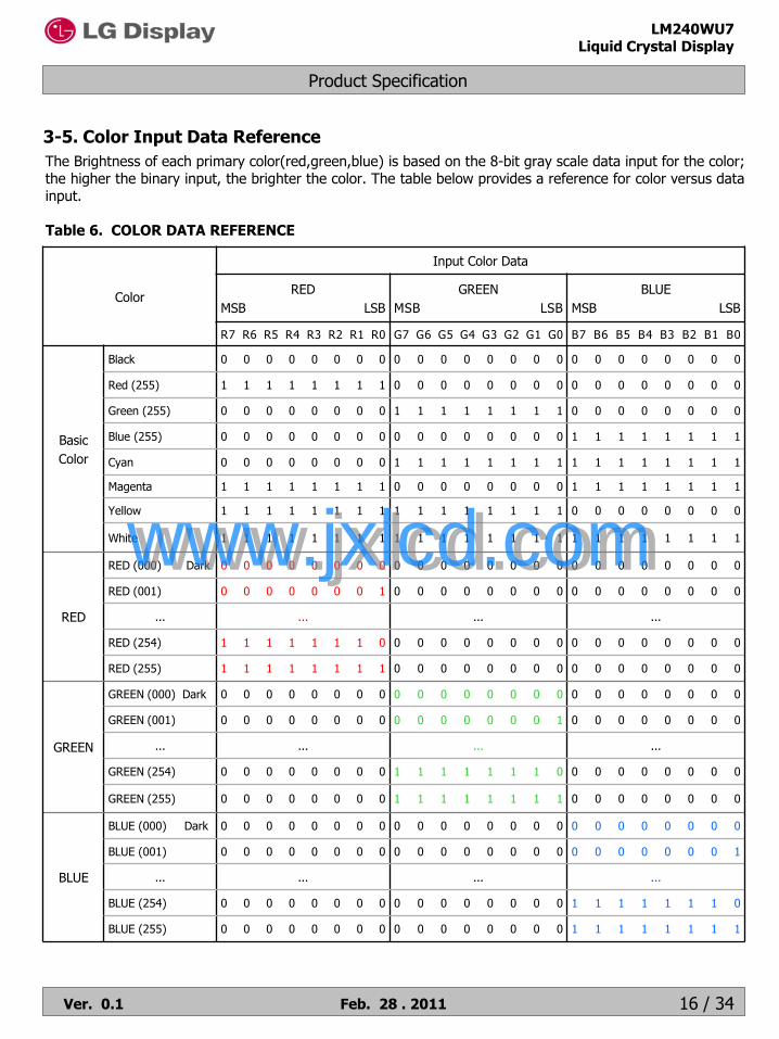
3-5. Color Input Data Reference
Table 6. COLOR DATA REFERENCE
The Brightness of each primary color(red,green,blue) is based on the 8-bit gray scale data input for the color;the higher the binary input, the brighter the color. The table below provides a reference for color versus datainput.
Color
Input Color Data
RED
MSB LSB
GREEN
MSB LSB
BLUE
MSB LSB
R7 R6 R5 R4 R3 R2 R1 R0 G7 G6 G5 G4 G3 G2 G1 G0 B7 B6 B5 B4 B3 B2 B1 B0
Basic
Color
Black 0 0 0 0 0 0 0 0 0 0 0 0 0 0 0 0 0 0 0 0 0 0 0 0
Red (255) 1 1 1 1 1 1 1 1 0 0 0 0 0 0 0 0 0 0 0 0 0 0 0 0
Green (255) 0 0 0 0 0 0 0 0 1 1 1 1 1 1 1 1 0 0 0 0 0 0 0 0
Blue (255) 0 0 0 0 0 0 0 0 0 0 0 0 0 0 0 0 1 1 1 1 1 1 1 1
Cyan 0 0 0 0 0 0 0 0 1 1 1 1 1 1 1 1 1 1 1 1 1 1 1 1
Magenta 1 1 1 1 1 1 1 1 0 0 0 0 0 0 0 0 1 1 1 1 1 1 1 1
Yellow 1 1 1 1 1 1 1 1 1 1 1 1 1 1 1 1 0 0 0 0 0 0 0 0
White 1 1 1 1 1 1 1 1 1 1 1 1 1 1 1 1 1 1 1 1 1 1 1 1
RED
RED (000) Dark 0 0 0 0 0 0 0 0 0 0 0 0 0 0 0 0 0 0 0 0 0 0 0 0
RED (001) 0 0 0 0 0 0 0 1 0 0 0 0 0 0 0 0 0 0 0 0 0 0 0 0
... ... ... ...
RED (254) 1 1 1 1 1 1 1 0 0 0 0 0 0 0 0 0 0 0 0 0 0 0 0 0
RED (255) 1 1 1 1 1 1 1 1 0 0 0 0 0 0 0 0 0 0 0 0 0 0 0 0
GREEN
GREEN (000) Dark 0 0 0 0 0 0 0 0 0 0 0 0 0 0 0 0 0 0 0 0 0 0 0 0
GREEN (001) 0 0 0 0 0 0 0 0 0 0 0 0 0 0 0 1 0 0 0 0 0 0 0 0
... ... ... ...
GREEN (254) 0 0 0 0 0 0 0 0 1 1 1 1 1 1 1 0 0 0 0 0 0 0 0 0
GREEN (255) 0 0 0 0 0 0 0 0 1 1 1 1 1 1 1 1 0 0 0 0 0 0 0 0
BLUE
BLUE (000) Dark 0 0 0 0 0 0 0 0 0 0 0 0 0 0 0 0 0 0 0 0 0 0 0 0
BLUE (001) 0 0 0 0 0 0 0 0 0 0 0 0 0 0 0 0 0 0 0 0 0 0 0 1
... ... ... ...
BLUE (254) 0 0 0 0 0 0 0 0 0 0 0 0 0 0 0 0 1 1 1 1 1 1 1 0
BLUE (255) 0 0 0 0 0 0 0 0 0 0 0 0 0 0 0 0 1 1 1 1 1 1 1 1
www.jxlcd.comwww.jxlcd.com
Product Specification
LM240WU7Liquid Crystal Display
Ver. 0.1 Feb. 28 . 2011 17 / 34
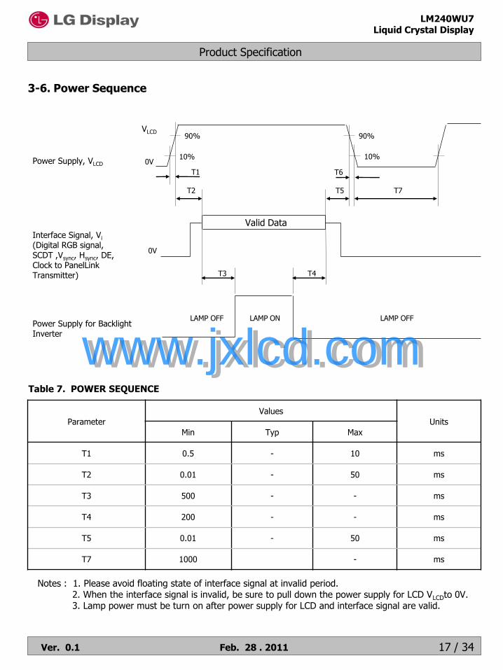
3-6. Power Sequence
Notes : 1. Please avoid floating state of interface signal at invalid period.2. When the interface signal is invalid, be sure to pull down the power supply for LCD VLCDto 0V.3. Lamp power must be turn on after power supply for LCD and interface signal are valid.
Interface Signal, Vi
(Digital RGB signal, SCDT ,Vsync, Hsync, DE, Clock to PanelLink Transmitter)
Power Supply for Backlight Inverter
Power Supply, VLCD
90%VLCD
90%
10% 10%
T1
0V
LAMP ONLAMP OFF
Parameter
Values
Units
Min Typ Max
T1 0.5 - 10 ms
T2 0.01 - 50 ms
T3 500 - - ms
T4 200 - - ms
T5 0.01 - 50 ms
T7 1000 - ms
Table 7. POWER SEQUENCE
T3
0V
T6
LAMP OFF
T4
T2 T5 T7
Valid Data
www.jxlcd.comwww.jxlcd.com
Product Specification
LM240WU7Liquid Crystal Display
Ver. 0.1 Feb. 28 . 2011 18 / 34
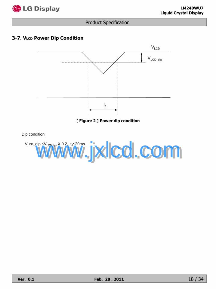
3-7. VLCD Power Dip Condition
Dip condition
VLCD_dip ≤VLCD_typ X 0.2, td≤20ms
VLCD
td
[ Figure 2 ] Power dip condition
VLCD_dip
www.jxlcd.comwww.jxlcd.com
Product Specification
LM240WU7Liquid Crystal Display
Ver. 0.1 Feb. 28 . 2011 19 / 34
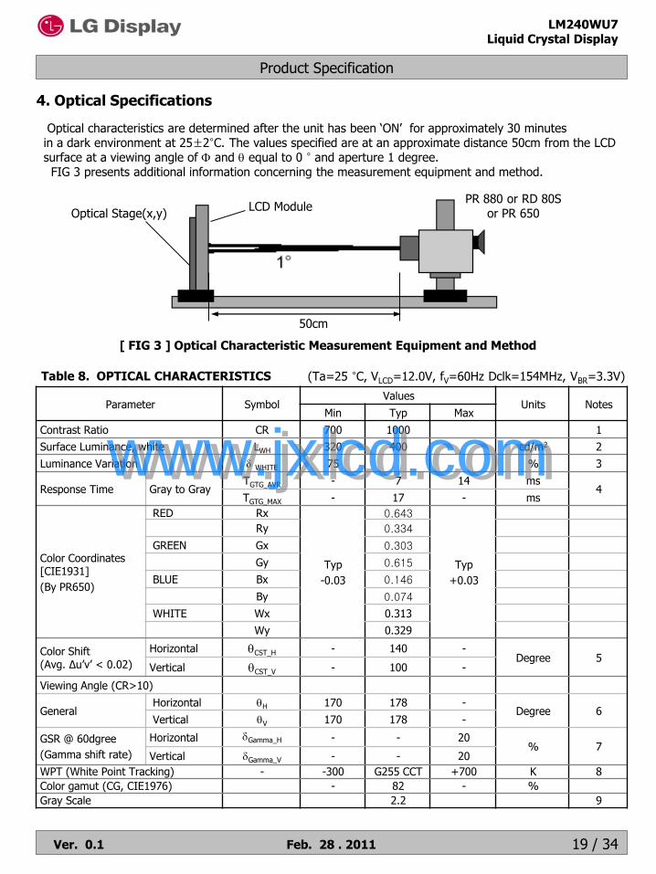
Optical characteristics are determined after the unit has been „ON‟ for approximately 30 minutesin a dark environment at 25±2°C. The values specified are at an approximate distance 50cm from the LCDsurface at a viewing angle of and equal to 0 ° and aperture 1 degree.FIG 3 presents additional information concerning the measurement equipment and method.
[ FIG 3 ] Optical Characteristic Measurement Equipment and Method
Table 8. OPTICAL CHARACTERISTICS (Ta=25 °C, VLCD=12.0V, fV=60Hz Dclk=154MHz, VBR=3.3V)
4. Optical Specifications
50cm
Optical Stage(x,y)LCD Module
PR 880 or RD 80S or PR 650
Parameter SymbolValues
Units NotesMin Typ Max
Contrast Ratio CR 700 1000 1
Surface Luminance, white LWH 320 400 cd/m2 2
Luminance Variation WHITE 75 % 3
Response Time Gray to GrayTGTG_AVR - 7 14 ms
4TGTG_MAX - 17 - ms
Color Coordinates [CIE1931]
(By PR650)
RED Rx
Typ
-0.03
0.643
Typ
+0.03
Ry 0.334
GREEN Gx 0.303
Gy 0.615
BLUE Bx 0.146
By 0.074
WHITE Wx 0.313
Wy 0.329
Color Shift(Avg. Δu‟v‟ < 0.02)
Horizontal CST_H - 140 -Degree 5
Vertical CST_V - 100 -
Viewing Angle (CR>10)
GeneralHorizontal H 170 178 -
Degree 6Vertical V 170 178 -
GSR @ 60dgree
(Gamma shift rate)
Horizontal Gamma_H - - 20% 7
Vertical Gamma_V - - 20
WPT (White Point Tracking) - -300 G255 CCT +700 K 8
Color gamut (CG, CIE1976) - 82 - %
Gray Scale 2.2 9
www.jxlcd.comwww.jxlcd.com

Product Specification
LM240WU7Liquid Crystal Display
Ver. 0.1 Feb. 28 . 2011 20 / 34
Notes 1. Contrast Ratio(CR) is defined mathematically as : (By PR880)
It is measured at center point(Location P1)
2. Surface luminance(LWH)is luminance value at 5 points average across the LCD surface 50cm from the surface with all pixels displaying white. For more information see FIG 2. (By PR880)LWH = = Average[ Lon1,Lon2,Lon3,Lon4,Lon5]
3. The variation in surface luminance , WHITE is defined as : (By PR880)
Where L1 to L9 are the luminance with all pixels displaying white at 9 locations. For more information see FIG 2.
4. Gray to gray response time is the time required for the display to transition from gray to gray. For additional information see Table 10. (By RD80S)
5. Color shift is the angle at which the average color difference for all Macbeth is lower than 0.02.For more information see FIG 3 and FIG 4. (By EZ Contrast)
- Color difference (Δu‟v‟)
u‟1, v‟1 : u‟v‟ value at viewing angle directionu‟2, v‟2 : u‟v‟ value at front (θ=0)i : Macbeth chart number (Define 22 page)
- Pattern size : 25% Box size- Viewing angle direction of color shift : Horizontal, Vertical
6. Viewing angle is the angle at which the contrast ratio is greater than 10. The angles aredetermined for the horizontal or x axis and the vertical or y axis with respect to the z axis whichis normal to the LCD surface. For more information see FIG 4. (By PR880)
7. GSR is the rate of gamma shift at up, down, left and right 60 degree viewing angle compare with center gamma. For more information see FIG 5 and FIG 6 (By EZ Contrast)
- GSR ( Gamma ) is defined as :
8. WPT (White Point Tracking) is the variation of color temperature between G255 and G63.(By PR650)
pixels black all with Luminance Surface
pixels white all with Luminance SurfaceRatioContrast
100)L .... ,L ,(L Maximum
)L .. ,L,Minimum(L
P9P2P1
P9P2P1
WHITE
3122
4'
yx
xu
3122
9'
yx
yv 2
21
2
21 )''()''('' vvuuvu
24
)''(
)''(
24
1
i
ivu
vuAvg
100Degree) (0 Value GammaCenter
Degree) 60Light Reft, Down, (Up, Value Gamma angle View1
GSR
www.jxlcd.comwww.jxlcd.com
Product Specification
LM240WU7Liquid Crystal Display
Ver. 0.1 Feb. 28 . 2011 21 / 34
Measuring point for surface luminance & measuring point for luminance variation.
FIG. 2 Measure Point for Luminance
H : 518.4 mmV : 324.0 mm
H
H/2
V
V/2
●
P1
P4P2
P9P7
●
●
● ●
●P3
●P8
P6●
P5●
H/10
V/1
0
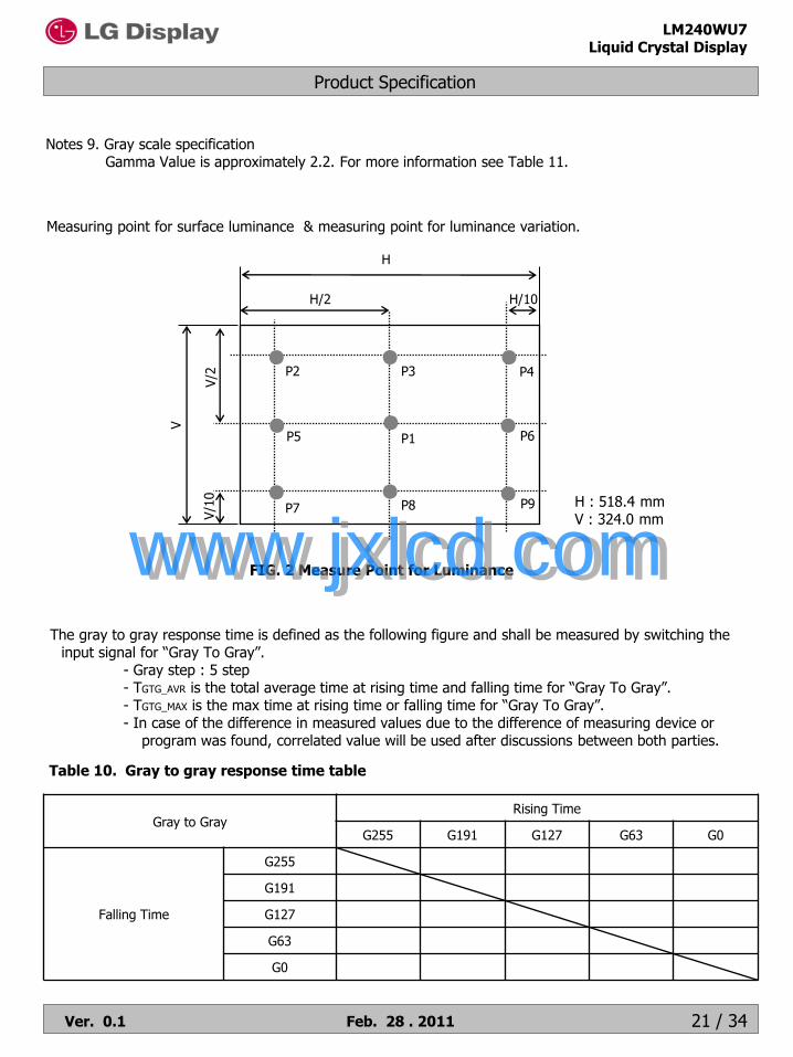
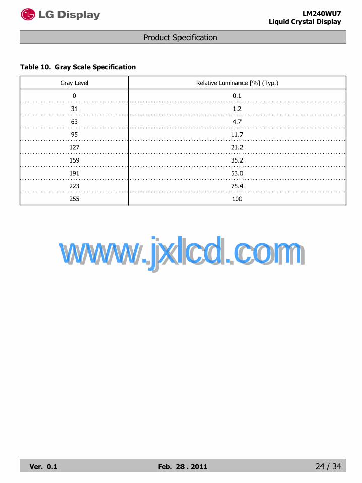
Notes 9. Gray scale specificationGamma Value is approximately 2.2. For more information see Table 11.
The gray to gray response time is defined as the following figure and shall be measured by switching the input signal for “Gray To Gray”.
- Gray step : 5 step- TGTG_AVR is the total average time at rising time and falling time for “Gray To Gray”.- TGTG_MAX is the max time at rising time or falling time for “Gray To Gray”.- In case of the difference in measured values due to the difference of measuring device or
program was found, correlated value will be used after discussions between both parties.
Table 10. Gray to gray response time table
Gray to GrayRising Time
G255 G191 G127 G63 G0
Falling Time
G255
G191
G127
G63
G0
www.jxlcd.comwww.jxlcd.com
Product Specification
LM240WU7Liquid Crystal Display
Ver. 0.1 Feb. 28 . 2011 22 / 34
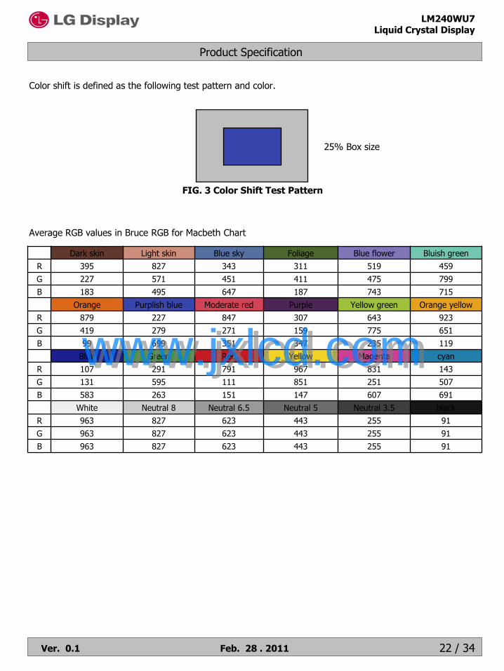
25% Box size
Average RGB values in Bruce RGB for Macbeth Chart
FIG. 3 Color Shift Test Pattern
Color shift is defined as the following test pattern and color.
Dark skin Light skin Blue sky Foliage Blue flower Bluish green
R 395 827 343 311 519 459
G 227 571 451 411 475 799
B 183 495 647 187 743 715
Orange Purplish blue Moderate red Purple Yellow green Orange yellow
R 879 227 847 307 643 923
G 419 279 271 159 775 651
B 99 699 351 347 235 119
Blue Green Red Yellow Magenta cyan
R 107 291 791 967 831 143
G 131 595 111 851 251 507
B 583 263 151 147 607 691
White Neutral 8 Neutral 6.5 Neutral 5 Neutral 3.5 black
R 963 827 623 443 255 91
G 963 827 623 443 255 91
B 963 827 623 443 255 91
www.jxlcd.comwww.jxlcd.com
Product Specification
LM240WU7Liquid Crystal Display
Ver. 0.1 Feb. 28 . 2011 23 / 34
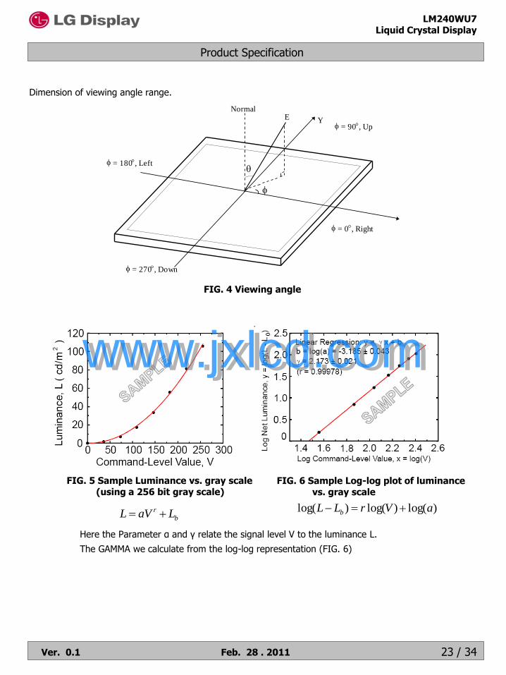
FIG. 4 Viewing angle
Dimension of viewing angle range.
Normal
Y E
= 0, Right
= 180, Left
= 270, Down
= 90, Up
b
r LaVL )log()log()log( aVrLL b
Here the Parameter α and γ relate the signal level V to the luminance L.
The GAMMA we calculate from the log-log representation (FIG. 6)
FIG. 5 Sample Luminance vs. gray scale (using a 256 bit gray scale)
FIG. 6 Sample Log-log plot of luminance vs. gray scale
www.jxlcd.comwww.jxlcd.com
Product Specification
LM240WU7Liquid Crystal Display
Ver. 0.1 Feb. 28 . 2011 24 / 34
Table 10. Gray Scale Specification
Gray Level Relative Luminance [%] (Typ.)
0 0.1
31 1.2
63 4.7
95 11.7
127 21.2
159 35.2
191 53.0
223 75.4
255 100
www.jxlcd.comwww.jxlcd.com
Product Specification
LM240WU7Liquid Crystal Display
Ver. 0.1 Feb. 28 . 2011 25 / 34
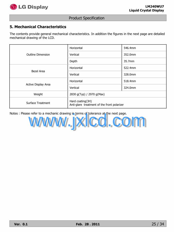
5. Mechanical Characteristics
The contents provide general mechanical characteristics. In addition the figures in the next page are detailed mechanical drawing of the LCD.
Outline Dimension
Horizontal 546.4mm
Vertical 352.0mm
Depth 35.7mm
Bezel AreaHorizontal 522.4mm
Vertical 328.0mm
Active Display AreaHorizontal 518.4mm
Vertical 324.0mm
Weight 2830 g(Typ) / 2970 g(Max)
Surface TreatmentHard coating(3H)Anti-glare treatment of the front polarizer
Notes : Please refer to a mechanic drawing in terms of tolerance at the next page.
www.jxlcd.comwww.jxlcd.com

Product Specification
LM240WU7Liquid Crystal Display
Ver. 0.1 Feb. 28 . 2011 26 / 34
<FRONT VIEW>
www.jxlcd.comwww.jxlcd.com
Product Specification
LM240WU7Liquid Crystal Display
Ver. 0.1 Feb. 28 . 2011 27 / 34
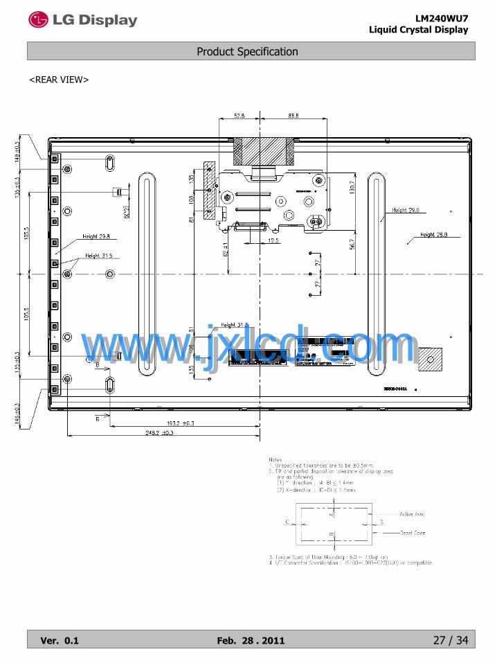
<REAR VIEW>
www.jxlcd.comwww.jxlcd.com
Product Specification
LM240WU7Liquid Crystal Display
Ver. 0.1 Feb. 28 . 2011 28 / 34
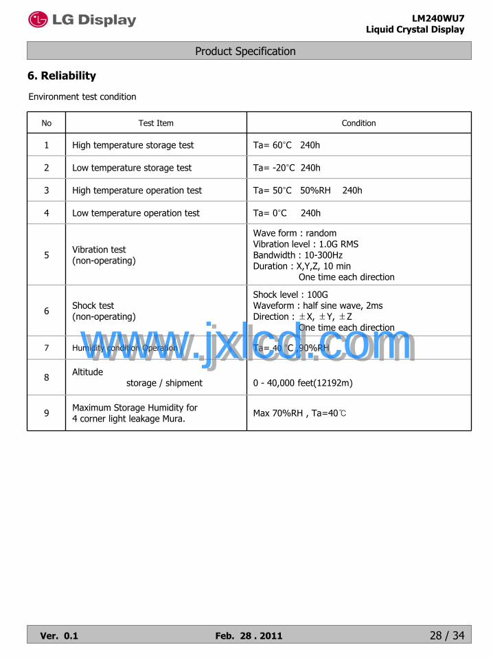
6. Reliability
Environment test condition
No Test Item Condition
1 High temperature storage test Ta= 60°C 240h
2 Low temperature storage test Ta= -20°C 240h
3 High temperature operation test Ta= 50°C 50%RH 240h
4 Low temperature operation test Ta= 0°C 240h
5Vibration test(non-operating)
Wave form : randomVibration level : 1.0G RMSBandwidth : 10-300HzDuration : X,Y,Z, 10 min
One time each direction
6Shock test(non-operating)
Shock level : 100GWaveform : half sine wave, 2msDirection : ±X, ±Y, ±Z
One time each direction
7 Humidity condition Operation Ta= 40 °C ,90%RH
8Altitude
storage / shipment 0 - 40,000 feet(12192m)
9Maximum Storage Humidity for4 corner light leakage Mura.
Max 70%RH , Ta=40℃
www.jxlcd.comwww.jxlcd.com
Product Specification
LM240WU7Liquid Crystal Display
Ver. 0.1 Feb. 28 . 2011 29 / 34
7. International Standards
7-1. Safety
7-2. EMC
a) ANSI C63.4 “Methods of Measurement of Radio-Noise Emissions from Low-Voltage Electrical andElectrical Equipment in the Range of 9kHZ to 40GHz. “American National Standards Institute(ANSI),1992
b) C.I.S.P.R “Limits and Methods of Measurement of Radio Interface Characteristics of InformationTechnology Equipment.“ International Special Committee on Radio Interference.
c) EN 55022 “Limits and Methods of Measurement of Radio Interface Characteristics of InformationTechnology Equipment.“ European Committee for Electrotechnical Standardization.(CENELEC), 1998( Including A1: 2000 )
a) UL 60950-1:2003, First Edition, Underwriters Laboratories, Inc.,Standard for Safety of Information Technology Equipment.
b) CAN/CSA C22.2, No. 60950-1-03 1st Ed. April 1, 2003, Canadian Standards Association,Standard for Safety of Information Technology Equipment.
c) EN 60950-1:2001, First Edition, European Committee for Electrotechnical Standardization(CENELEC)European Standard for Safety of Information Technology Equipment.
7-3. Environment
a) RoHS. Directive 2002/95/EC of the European Parliament and of the Council on the reduction of theuse of certain hazardous substances in electrical and electronic equipment. January 2003
www.jxlcd.comwww.jxlcd.com
Product Specification
LM240WU7Liquid Crystal Display
Ver. 0.1 Feb. 28 . 2011 30 / 34
8. Packing
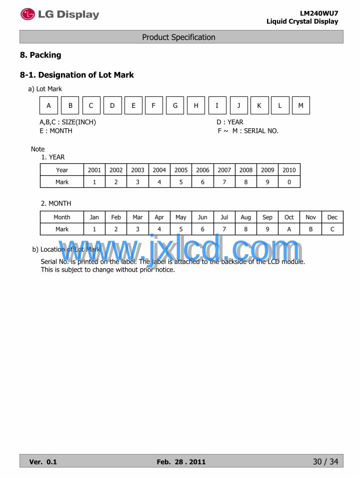
8-1. Designation of Lot Mark
a) Lot Mark
A B C D E F G H I J K L M
A,B,C : SIZE(INCH) D : YEAR
E : MONTH F ~ M : SERIAL NO.
Note1. YEAR
2. MONTH
Mark
Year
0
2010
6
2006
7
2007
8
2008
9
2009
4
2004
5
2005
321
200320022001
B
Nov
Mark
Month
A
Oct
6
Jun
7
Jul
8
Aug
9
Sep
4
Apr
5
May
C321
DecMarFebJan
b) Location of Lot Mark
Serial No. is printed on the label. The label is attached to the backside of the LCD module.This is subject to change without prior notice.
www.jxlcd.comwww.jxlcd.com
Product Specification
LM240WU7Liquid Crystal Display
Ver. 0.1 Feb. 28 . 2011 31 / 34
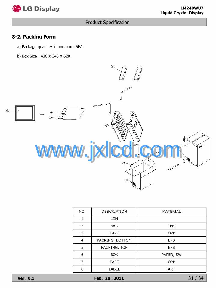
a) Package quantity in one box : 5EA
b) Box Size : 436 X 346 X 628
8-2. Packing Form
NO. DESCRIPTION MATERIAL
1 LCM
2 BAG PE
3 TAPE OPP
4 PACKING, BOTTOM EPS
5 PACKING, TOP EPS
6 BOX PAPER, SW
7 TAPE OPP
8 LABEL ART
www.jxlcd.comwww.jxlcd.com

Product Specification
LM240WU7Liquid Crystal Display
Ver. 0.1 Feb. 28 . 2011 32 / 34
8-3. Pallet Form
NO. DESCRIPTION MATERIAL
1 PACKING ASS’Y
2 PALLET PLYWOOD_1140X990X120
3 ANGLE, PACKING SWR4
4 LABEL YUPO PAPER
5 BAND PP
6 BAND, CLIP CLIP 18MM
www.jxlcd.comwww.jxlcd.com

Product Specification
LM240WU7Liquid Crystal Display
Ver. 0.1 Feb. 28 . 2011 33 / 34
9. PRECAUTIONS
Please pay attention to the followings when you use this TFT LCD module.
9-1. MOUNTING PRECAUTIONS
(1) You must mount a module using holes arranged in four corners or four sides.(2) You should consider the mounting structure so that uneven force (ex. Twisted stress) is not applied to the
module. And the case on which a module is mounted should have sufficient strength so that external force is not transmitted directly to the module.
(3) Please attach the surface transparent protective plate to the surface in order to protect the polarizer.Transparent protective plate should have sufficient strength in order to the resist external force.
(4) You should adopt radiation structure to satisfy the temperature specification.(5) Acetic acid type and chlorine type materials for the cover case are not desirable because the former
generates corrosive gas of attacking the polarizer at high temperature and the latter causes circuit break by electro-chemical reaction.
(6) Do not touch, push or rub the exposed polarizers with glass, tweezers or anything harder than HBpencil lead. And please do not rub with dust clothes with chemical treatment.Do not touch the surface of polarizer for bare hand or greasy cloth.(Some cosmetics are detrimentalto the polarizer.)
(7) When the surface becomes dusty, please wipe gently with absorbent cotton or other soft materials like chamois soaks with petroleum benzene. Normal-hexane is recommended for cleaning the adhesives used to attach front / rear polarizers. Do not use acetone, toluene and alcohol because they cause chemical damage to the polarizer.
(8) Wipe off saliva or water drops as soon as possible. Their long time contact with polarizer causes deformations and color fading.
(9) Do not open the case because inside circuits do not have sufficient strength.
9-2. OPERATING PRECAUTIONS
(1) The spike noise causes the mis-operation of circuits. It should be lower than following voltage : V=±200mV(Over and under shoot voltage)
(2) Response time depends on the temperature.(In lower temperature, it becomes longer.)(3) Brightness depends on the temperature. (In lower temperature, it becomes lower.)
And in lower temperature, response time(required time that brightness is stable after turned on) becomeslonger.
(4) Be careful for condensation at sudden temperature change. Condensation makes damage to polarizer or electrical contacted parts. And after fading condensation, smear or spot will occur.
(5) When fixed patterns are displayed for a long time, remnant image is likely to occur.(6) Module has high frequency circuits. Sufficient suppression to the electromagnetic interference shall be
done by system manufacturers. Grounding and shielding methods may be important to minimized theinterference.
(7) Please do not give any mechanical and/or acoustical impact to LCM. Otherwise, LCM can‟t be operated its full characteristics perfectly.
(8) A screw which is fastened up the steels should be a machine screw. (if not, it causes metallic foreign material and deal LCM a fatal blow)
(9) Please do not set LCD on its edge.(10) When LCMs are used for public display defects such as Yogure, image sticking can not be guarantee.
www.jxlcd.comwww.jxlcd.com
Product Specification
LM240WU7Liquid Crystal Display
Ver. 0.1 Feb. 28 . 2011 34 / 34
Since a module is composed of electronic circuits, it is not strong to electrostatic discharge. Make certain thattreatment persons are connected to ground through wrist band etc. And don‟t touch interface pin directly.
9-3. ELECTROSTATIC DISCHARGE CONTROL
Strong light exposure causes degradation of polarizer and color filter.
9-4. PRECAUTIONS FOR STRONG LIGHT EXPOSURE
When storing modules as spares for a long time, the following precautions are necessary.
(1) Store them in a dark place. Do not expose the module to sunlight or fluorescent light. Keep the temperature between 5°C and 35°C at normal humidity.
(2) The polarizer surface should not come in contact with any other object.It is recommended that they be stored in the container in which they were shipped.
9-5. STORAGE
9-6. HANDLING PRECAUTIONS FOR PROTECTION FILM
(1) The protection film is attached to the bezel with a small masking tape.When the protection film is peeled off, static electricity is generated between the film and polarizer.This should be peeled off slowly and carefully by people who are electrically grounded and with well ion-blown equipment or in such a condition, etc.
(2) When the module with protection film attached is stored for a long time, sometimes there remains a very small amount of glue still on the bezel after the protection film is peeled off.
(3) You can remove the glue easily. When the glue remains on the bezel surface or its vestige is recognized, please wipe them off with absorbent cotton waste or other soft material like chamois soaked with normal-hexane.
www.jxlcd.comwww.jxlcd.com